

Page 1
MIC74 Micrel
MIC74
2-Wire Serial I/O Expander and Fan Controller
Advance Information
General Description
The MIC74 is a fully programmable serial-to-parallel I/O
expander compatible with the SMBus™ (system management bus) protocol. It acts as a “slave” on the bus, providing
eight independent I/O lines.
Each I/O bit can be individually programmed as an input or
output. If programmed as an output, each I/O bit can be
programmed as an open-drain or complementary push-pull
output. If desired, the four most significant I/O bits can be
programmed to implement fan speed control. An internal
clock generator and state machine eliminate the overhead
generally associated with “bit-banging” fan speed control.
Programming the device and reading/writing the I/O bits is
accomplished using seven internal registers. All registers can
be read by the host. Output bits are capable of directly driving
high-current loads such as LEDs. A separate interrupt output
can notify the host of state changes on the input bits without
requiring the MIC74 to perform a transaction on the serial bus
or be polled by the host. Three address selection inputs are
provided, allowing up to eight devices to share the same bus
and provide a total of 64 bits of I/O.
The MIC74 is available in an ultra-small-footprint 16-lead
QSOP. Low quiescent current, small footprint, and low package height make the MIC74 ideal for portable and desktop
applications.
Features
• Provides eight bits of general purpose I/O
• Built in fan speed control logic (optional)
• 2-wire SMBus™/I2C™ compatible serial interface
plus interrupt output
• 2.7V to 3.6V operating voltage range
• 5V-tolerant I/O
• Low quiescent current: 2µA (typical)
• Bit-programmable I/O options:
input or output
push-pull or open-drain output
interrupt on input changes
• Outputs can directly drive LEDs (10mA IOL)
• Up to 8 devices per bus
Applications
• General purpose I/O expansion via serial bus
• Personal computer system management
• Distributed sensing and control
• Microcontroller I/O expansion
• Fan Control
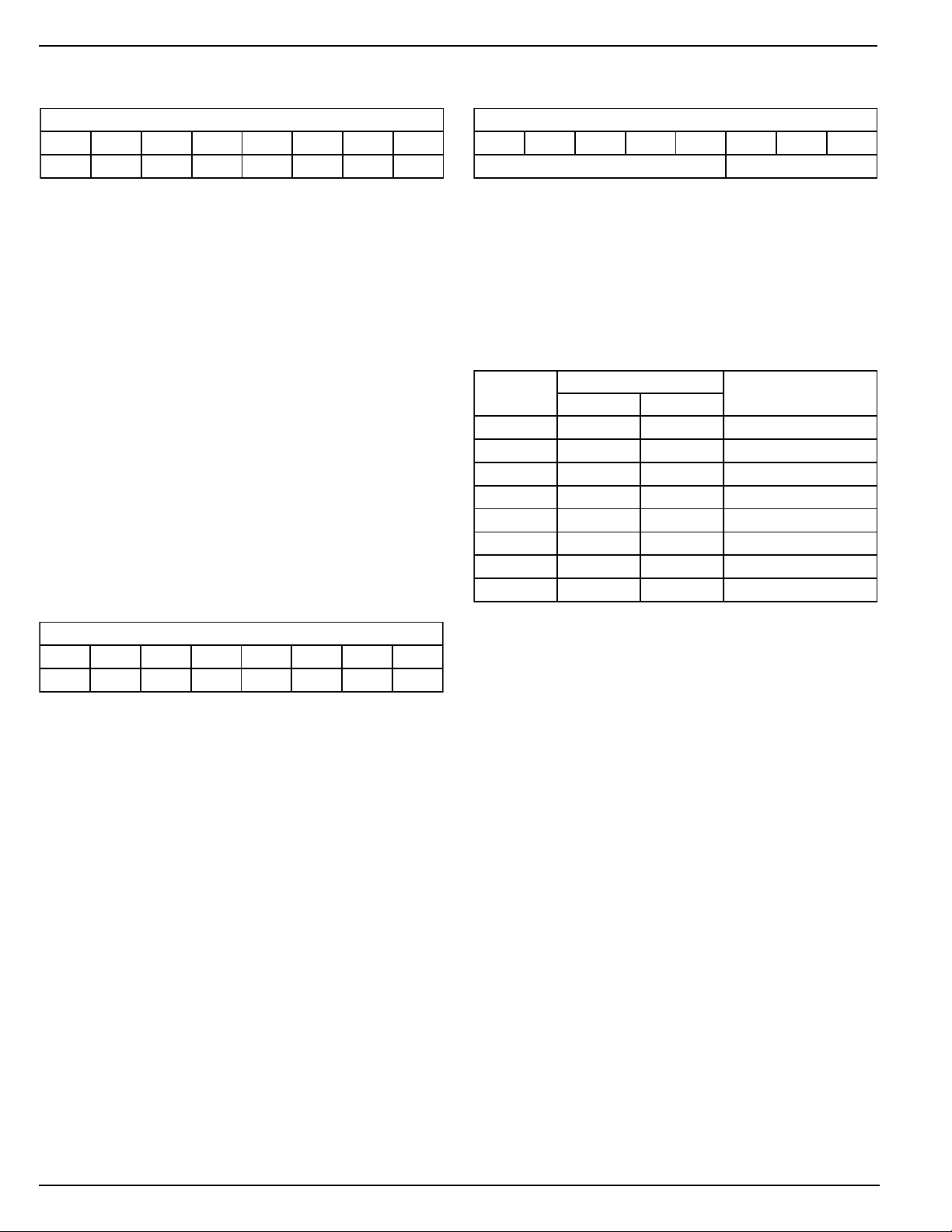
Ordering Information
Part Number Temperature Range Package
MIC74BQS –40°C to +85°C 16-lead QSOP
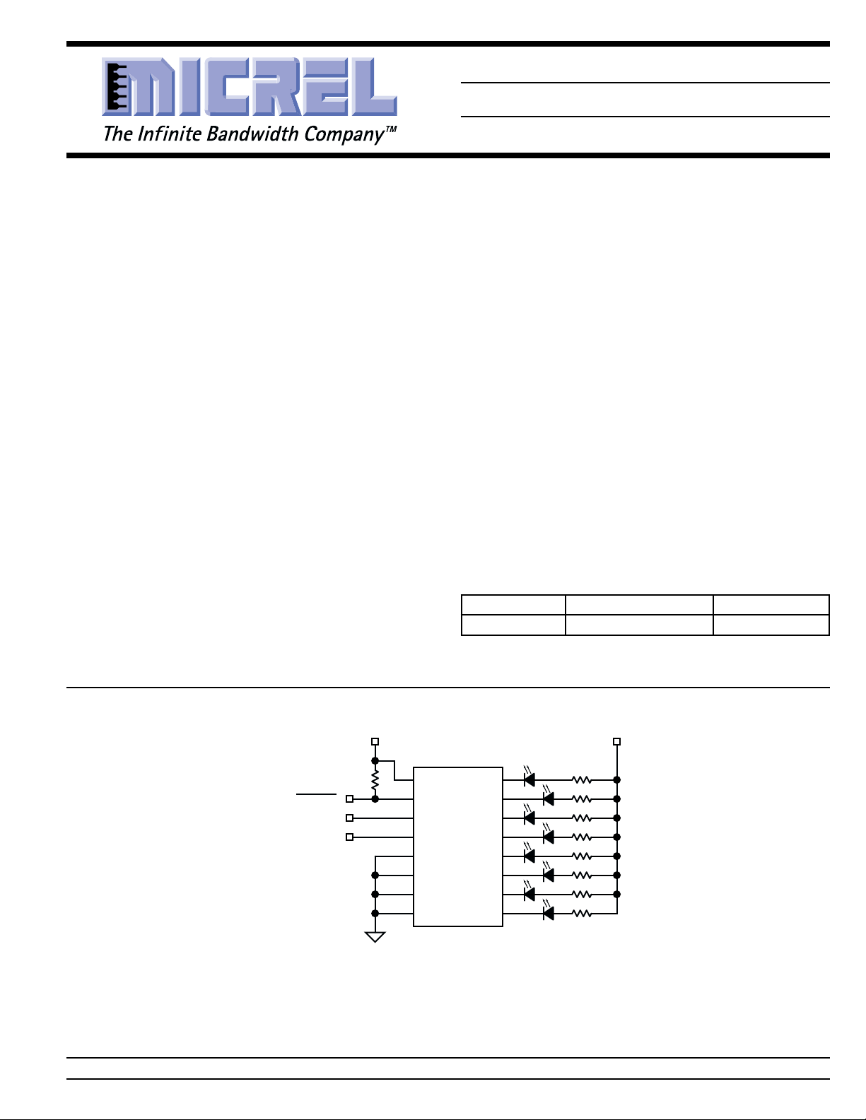
Typical Application
3.0V3.0V
MIC74
R9
ALERT
DATA
CLK
VDD
/ALERT
DATA
CLK
A0
A1
A2
GND
P0
P1
P2
P3
P4
P5
P6
P7
LED8
Serial-Bus-Controlled LED Annunciator
SMBus™ is a trademark of Intel Corporation. I2C™ is a trademark of Phillips Electronics N.V.
Micrel, Inc. • 1849 Fortune Drive • San Jose, CA 95131 • USA • tel + 1 (408) 944-0800 • fax + 1 (408) 944-0970 • http://www.micrel.com
August 1, 2000 1 MIC74
R1LED1
R2
R3
R4
R5
R6
R7
R8
Page 2
MIC74 Micrel
Pin Configuration
A1
A2
P0
P1
P2
P3
GND
Pin Description
Pin Number Pin Name Pin Function
1–3A0–A2 Address (Input): Slave address selection inputs; sets the three least signifi-
4–7P0–P3 Parallel I/O (Input/Output): General-purpose I/O pin. Direction and output
8 GND Ground
9–12
13 /ALERT Interrupt (Output): Active-low, open-drain output signals input-change-
14 CLK Serial Bus Clock (Input): The host provides the serial bit clock in this input.
15 DATA Serial Data (Input/Output): Serial data input and open-drain serial data
16 VDD Power Supply (Input.)
P4–P7 (/SHDN, /FS0–/FS2)
1A0
2
3
4
5
6
7
8
16 VDD
DATA
15
CLK
14
/ALERT
13
P7 (/FS2)
12
P6 (/FS1)
11
P5 (/FS0)
10
P4 (/SHDN0)
9
16-Lead QSOP
cant bits of the MIC74’s slave address.
type are user programmable.
Parallel I/O (Input/output): P4–P7 are general-purpose I/O pins. Direction
and output type are user programmable.
Shutdown (Output): When the FAN bit is set, pin 9 becomes SHDN.
Fan Speed (Output): When the FAN bit is set, pins 10 through 12 become /
FS0–/FS2 respectively, controlled by the FAN_SPEED register.
interrupts to the host on this pin. Signal is cleared when the bus master
(host) polls the ARA (alert response address = 0001 100) or reads status.
output.
MIC74 2 August 1, 2000
Page 3

MIC74 Micrel
Absolute Maximum Ratings (Note 1)
Supply Voltage (V
Input Voltage
VDD and GND]
Junction Temperature (T
) .................................................+4.6V
DD
[all pins except
(VIN) ........................ GND – 0.3V to 5.5V
) ...................................... +150°C
J
Operating Ratings (Note 2)
Supply Voltage (V
Ambient Temperature (T
Package Thermal Resistance ............................... 163°C/W
) .................................. +2.7V to +3.6V
DD
) ......................... –40°C to +85°C
A
Lead Temperature (10 sec.).................................... +260°C
ESD Rating, Note 3
V
...........................................................................................
DD
1.5kV
A0,A1,A2 .................................................................500V
Others ..................................................................... 200V
Electrical Characteristics
2.7V ≤ VDD ≤ 3.6V; TA = 25°C, bold values indicate –40°C ≤ TA ≤ +85°C; unless noted.
Symbol Parameter Condition Min Typ Max Units
V
IN
I
DD
I
START
I
STBY
Serial I/O (DATA, CLK)
V
IL
V
IH
V
OL
I
LEAK
C
IN
Parallel I/O [P0–P3, P4(/SHDN), P5(/FS0)–P7(/FS2)]
V
IL
V
IH
I
OL
I
OH
I
LEAK
C
IN
C
OUT
Address Input (A0–A2)
V
IL
V
IH
I
LEAK
Input Voltage, any pin except
GND–0.3
5.5 V
VDD and GND
Operating Supply Current P[7:0] inputs; P[7:0] = VDD or GND 2 6 µA
/ALERT open; f
Fan Startup Supply Current during t
(Fan Mode Only) /FS2[2:0] = open; V
START;
= 100kHz
CLK
/ALERT, /SHDN, 1.75 mA
SMBCLK
= V
SMBDATA
= VDD;
P[3:0] = inputs
Standby Supply Current /ALERT = open, V
SMBCLK
= V
SMBDATA
= VDD;13µA
P[3:0] = inputs
Input Low Voltage –0.3 0.8 V
Input High Voltage 2.0 5.5 V
Output Low Voltage IOL = 3mA 0.4 V
Leakage Current VIN = 5.5V or GND –1+1µA
Input Capacitance 10 pF
Input Low Voltage –0.5 0.8 V
Input High Voltage 2 5.5 V
Output Low Current VOL = 0.4V, VDD = 2.7V 7 mA
VOL = 1V, VDD = 3.3V 10 mA
Output High Current VOH = 2.4V 7 mA
Leakage Current VIN = 5.5V or GND –1+1µA
Input Capacitance 10 pF
Output Capacitance 10 pF
Input Low Voltage –0.3 0.3V
Input High Voltage 0.7V
Leakage Current VIN = V
or GND –250 +250 nA
DD
DD
VDD+0.3
DD
V
V
August 1, 2000 3 MIC74
Page 4
MIC74 Micrel
Symbol Parameter Condition Min Typ Max Units
/ALERT
V
OL
I
LEAK
AC Characteristics
t
START
t
PULSE
t
/INT
t
/IR
t
HD:STA
t
SU:STA
t
SU:STO
t
HD:DAT
t
SU:DAT
t
TIMEOUT
t
LOW
t
HIGH
t
F
t
R
t
BUF
Output Low Voltage IOL = 1mA 0.4 V
Leakage Current VIN = V
DD
or V
SS
–1 ±250 +1 µA
Fan Startup Interval normal operation 0.5 1 3.3 sec
Minimum Pulse-Width minimum pulse-width on Pn to 10 ns
generate an interrupt, Note 7
Interrupt Delay interrupt delay from state change 4 µs
on Pn to /ALERT ≤ VOL, Note 7
Delay from Status Read or ARA 4 µs
Response to /ALERT ≥ V
OH
Hold Time, Note 7 hold time after repeated start condition. 4.0 µs
after this period, the first clock is generated.
Setup Time, Note 7 repeated start condition setup time 4.7 µs
Stop Condition Setup Time Note 7 4.0 µs
Data Hold Time Note 7 500 ns
Data Setup Time Note 7 0ns
Clock Low Time-Out Notes 4, 7 25 35 ms
Clock Low Period Notes 5, 7 4.7 µs
Clock High Period Notes 5, 7 4.0 50 µs
Clock/Data Fall Time Notes 6, 7 300 ns
Clock/Data Rise Time Notes 6, 7 1000 ns
Bus free time between stop and Note 7 4.7 µs
Start condition
Note 1. Exceeding the absolute maximum rating may damage the device.
Note 2. The device is not guaranteed to function outside its operating rating.
Note 3. Devices are ESD sensitive. Handling precautions recommended. Human body model, 1.5k in series with 100pF.
Note 4. Devices participating in a transfer will timeout when any clock low exceeds the value of t
Note 5. t
Note 6. Rise and fall time is defined as follows: tR = V
Note 7. Guaranteed by design.
timeout condition must reset the communication no later than t
both a master and a slave as it incorporates the cumulative stretch limit for both a master (10ms) and a slave (25ms).
HIGH(max)
provides a simple guaranteed method for devices to detect bus idle conditions.
– 0.15V to V
IL(max)
TIMEOUT(max)
IH(min)
of 35ms. The maximum value specified must be adhered to by
+ 0.15V; tF = 0.9VDD to V
TIMEOUT(min)
of 25ms. Devices that have detected a
– 0.15V.
IL(max)
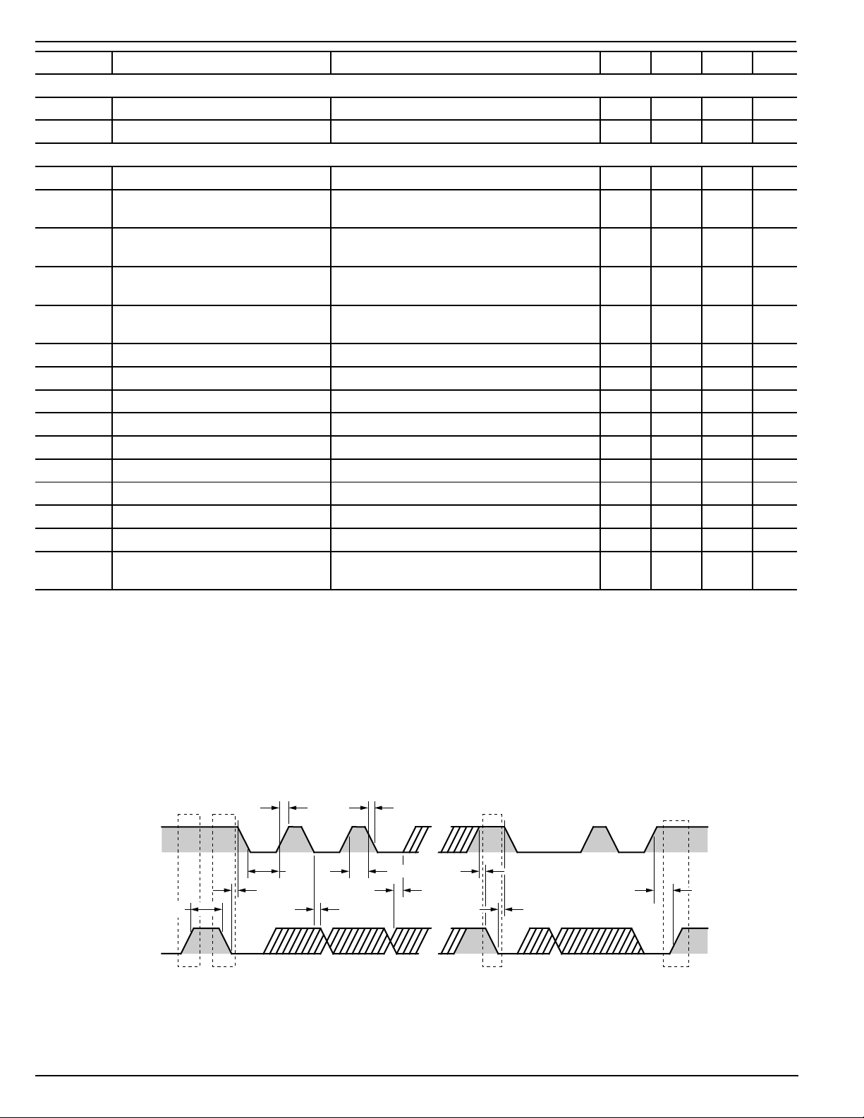
Timing Definitions
CLK
DATA
t
R
t
LOW
t
HD:STA
t
BUF
t
HD:DAT
StoP StoPStart Start
t
F
t
SU:DAT
t
HIGH
t
SU:STA
t
HD:STA
t
SU:STO
MIC74 4 August 1, 2000
Page 5
MIC74 Micrel
Register Descriptions
Device Configuration Register
GFC_VED
]7[D]6[D]5[D]4[D]3[D]2[D]1[D]0[D
.orezsaetirwsyawlANAFEI
Power-On Default Value: 0000 0000b, 00
h
Interrupts disabled
Not in Fan Mode
Command_byte addess: 0000 0000b, 00
h
Type: 8-bits, read/write
Bit Name: IE
Function: Global interrupt enable.
Operation: 1 = enabled
0 = disabled
Bit Name: FAN
Function: Selects Fan Mode
(P[7:4] vs. /FS[2:0], /SHDN)
Operation: 1 = Fan Mode
0 = I/O Mode
Output Configuration Register
GFC_TUO
]7[D]6[D]5[D]4[D]3[D]2[D]1[D]0[D
7TUO6TUO5TUO4TUO3TUO2TUO1TUO0TUO
Power-On Default Value: 0000 0000b, 00
h
all outputs open-drain
Command_byte addess: 0000 0010b, 02
h
Type: 8-bits, read/write
Bit Name: OUT
n
Function: Selects output driver configuration of Pn when
Pn is configured as an output.
Operation: 1 = push-pull
0 = open-drain
Notes: If Fan Mode is selected, that is, the FAN bit of
the DEV_CFG register is set to one, P[7:4] are
automatically configured as open-drain
outputs. They are then referred to as /FS[2:0]
and /SHDN. The OUT_CFG register has no
effect on these I/O bits while in Fan Mode.
Bit Name: D[2] through D[6]
Function: Reserved
Operation: Reserved—always write as zero
Data Direction Register
RID
]7[D]6[D]5[D]4[D]3[D]2[D]1[D]0[D
7RID6RID5RID4RID3RID2RID1RID0RID
Power-On Default Value: 0000 0000b, 00
h
all Pn’s configured as inputs
Command_byte addess: 0000 0001b, 01
h
Type: 8-bits, read/write
Bit Name: DIR
Function: Selects data direction, input or output, of P
n
n
Operation: 1 = output
0 = input
Notes: If Fan Mode is selected, that is, the FAN bit of
the DEV_CFG register is set to one, P[7:4] are
automatically configured as open-drain
outputs. They are then referred to as /FS[2:0]
and /SHDN. The DIR register has no effect on
these I/O bits while in Fan Mode.
Status Register
SUTATS
]7[D]6[D]5[D]4[D]3[D]2[D]1[D]0[D
7S6S5S4S3S2S1S0S
Power-On Default Value: 0000 0000b, 00
h
no interrupts pending
Command_byte addess: 0000 0011b, 03
h
Type: 8-bits, read only
Bit Name: S
n
Function: Flag for Pn input-change event when Pn is
configured as an input; Sn is set when the
corresponding input changes state.
Operation: 1 = change occured
0 = no change occured
Notes: If Fan Mode is selected, that is, the FAN bit of
the DEV_CFG register is set to one, P[7:4] are
automatically configured as open-drain
outputs. They are then referred to as /FS[2:0]
and /SHDN. No interrupts of any kind are
generated by these pins while in Fan Mode.
All status bits are cleared after any read
operation is performed on STATUS.
August 1, 2000 5 MIC74
Page 6
MIC74 Micrel
Interrupt Mask Register
KSAM_TNI
]7[D]6[D]5[D]4[D]3[D]2[D]1[D]0[D
7MI6MI5MI4MI3MI2MI1MI0MI
Power-On Default Value: 0000 0000b, 00
Command_byte addess: 0000 0100b, 04
h
h
Type: 8-bits, read/write
Bit Name: IM
n
Function: Interrupt enable bit for Pn when Pn is config-
ured as an input
Operation: 1 = enabled
0 = disabled
Notes: If Fan Mode is selected, that is, the FAN bit of
the DEV_CFG register is set to one, P[7:4] are
automatically configured as open-drain
outputs. They are then referred to as /FS[2:0]
and /SHDN. No interrupts of any kind are
generated by these pins while in Fan Mode.
Data Register
ATAD
]7[D]6[D]5[D]4[D]3[D]2[D]1[D]0[D
7P6P5P4P3P2P1P0P
Power-On Default Value: 1111 1111b, FF
Command_byte addess: 0000 0101b, 05
h
h
Type: 8-bits, read/write
Bit Name: P
n
Function: Returns the current state of any Pn configured
as an input and the last value written to Pn’s
configured as outputs; Writing the DATA
register sets the output state of any Pn’s
configured as outputs; writes to I/O bits
configured as inputs are ignored.
Read Operation: 1 = Pn is high
0 = Pn is low
Write Operation: 1 = Pn is set to one
0 = Pn is cleared
Notes: If Fan Mode is selected, that is, the FAN bit of
the DEV_CFG register is set to one, P[7:4] are
automatically configured as open-drain
outputs. They are then referred to as /FS[2:0]
and /SHDN. The state of these pins is determined by the FAN_SPEED register. While in
Fan Mode, D[7:4] of the DATA registers have
no effect.
Fan Speed Register
DEEPS_NAF
]7[D]6[D]5[D]4[D]3[D]2[D]1[D]0[D
.orezsaetirwsyawlAdeepSnaF
Power-On Default Value: 0000 0000b, 00
h
fan off
Command_byte addess: 0000 0110b, 06
h
Type: 8-bits, read/write
Bit Name: D[0] through D[2]
Function: Determines bit-pattern on FS[2:0]
Operation:
]0:2[D
eulaV
0001110 ffo
1000111 )tsewols(1deeps
0101011 2deeps
1100011 3deeps
0011101 4deeps
1010101 5deeps
0111001 6deeps
1110001 )tsetsaf(7deeps
]0:2[SF/NDHS/
etatStuptuO
deepSnaF
Fan Speed Settings
Notes: Any time the fan speed register contains zero,
that is, the fan is shut down, and a non-zero
value is written into the fan speed register, the
/FS[2:0] and /SHDN outputs will assume the
highest fan speed state for approximately one
second (t
). Following this interval, the
START
state of the fan speed control outputs will
assume the value indicated by the contents of
FAN_SPEED. This insures that the fan will
start reliably when low speed operation is
desired.
Bit Name: D[3] through D[7]
Function: Reserved
Operation: Always write as zero.
MIC74 6 August 1, 2000
Page 7

MIC74 Micrel
Functional Diagram
INT
n
IM
n
STATUS
STATUS_READ
OUT_CFG
(OUTPUT)
DATA
(INPUT)
DIR
DATA
n
n
n
n
n
n
SQ
QR
Typical I/O Port (Fan Speed Control Logic Not Shown)
Functional Description
Pin Descriptions
VDD
Power supply input connection. See “Operating Ratings.”
GND
Ground or return connection for all MIC74 functions.
CLK
An CLK signal is provided by the host (master) and is
common to all devices on the bus. The CLK signal controls all
transactions in both directions on the bus and is applied to
each MIC74 at the CLK pin.
DATA
Serial data is bidirectional and is common to all devices on the
bus. The MIC74’s DATA output is open-drain.
The DATA line requires one external pull-up resistor or
current source per system that can be located anywhere
along the line.
A2, A1, A0
An MIC74 responds to its own unique address which is
assigned using the A0–A2 pins. A0–A2 set the three LSBs
(least significant bits) of the MIC74’s 7-bit slave address. The
three address pins allow eight unique MIC74 addresses in a
system. When the MIC74’s address matches an address
received in the serial bit stream, communication is initiated.
A2, A1 and A0 should be connected to GND or VDD. The state
of these pins is sampled only once at device power-on. New
slave addresses are not accepted unless the MIC74 is
powered off then on.
EDGE
DETECT
V
DD
Pn (typical I/O port)
GND
stupnIsserddAevalS47CIM
2A1A0AyraniBxeH
000 0010 000
001 0010 100
010 0010 010
011 0010 110
100 0010 001
101 0010 101
110 0010 011
111 0010 111
b
b
b
b
b
b
b
b
02
h
12
h
22
h
32
h
42
h
52
h
62
h
72
h
Table 1. MIC74 Address Configuration
Alert Response Address
The MIC74 also responds to the ARA (Alert Response
Address). The ARA is used by the master (host) to request the
address of a slave that has provided an interrupt to the master
via the /ALERT line.
The ARA is a single address (0001 100) common to all slaves
and is described in more detail under “Interrupt Generation”
with related information under “/ALERT.” Also see Figure 7.
Pn, /SHDN, and /FS0–/FS2
P0 through P7 are general-purpose input/output bits. Each bit
is independently programmable as an input or an output. If
programmed as an output, each bit is further programmable
as either a complementary push-pull or open-drain output.
If properly enabled, any Pn programmed as an input will
generate an interrupt to the host using the /ALERT output
when the input changes state. In this way, the MIC74 can
August 1, 2000 7 MIC74
Page 8

MIC74 Micrel
notify the host of an input change without requiring periodic
polling by the host or a message transaction on the bus.
Regardless of whether interrupts are enabled or disabled,
each input-change event also sets the corresponding bit in
the status register. I/O configuration is performed using the
output configuration (OUT_CFG), I/O direction (DIR), and
interrupt mask (INT_MASK) registers.
If the FAN bit in the device configuration register is set, the
states of P[7:4] are controlled by the FAN_SPEED register.
The bits in the OUT_CFG, DIR, and INT_MASK registers
corresponding to P[7:4] are ignored. When in Fan Mode,
P[7:4] are referred to as /FS2, /FS1, /FS0, and /SHDN. While
in this mode, no interrupts of any kind will be generated by
these pins.
/ALERT
The alert signal is an open-drain, active-low output. The
operation of the /ALERT output is controlled by the IMn bits
in the INT_MASK register and the global interrupt enable bit
(IE) in the DEV_CFG register.
If the IE bit is set to zero, or if the corresponding interrupt
enable bit, IMn, is set to zero, no input-change interrupts will
be generated. (Regardless of the IE bit setting, the change
will be reflected in the status register.)
If the IE bit is set to one, IMn is set to one, and Pn is an input,
then /ALERT is driven active whenever Pn changes state,
(goes from a high-to-low or low-to-high state). Once triggered,
/ALERT is unconditionaly reset to its inactive state once the
MIC74 successfully responds to the alert response address
or STATUS is read.
Serial Port Operation
The MIC74 uses standard SMBus Read_Byte and Write_Byte
operations to communicate with its host.
The Read_Byte operation is a composite read-write operation consisting of first sending the MIC74’s slave address
followed by a command byte (a write) and then resending the
slave address and clocking out the data byte (a read). The
command byte is the address of the target register. See Table
2. An example of a Read_Byte operation is shown in Figure
8.
Similarly, the write-byte operation consists of sending the
device’s slave address followed by a command byte and the
byte to be written to the target register. Again, in the case of
the MIC74, the command byte is the address of the target
register. See Table 2.
In addition, to the read byte and write byte protocols, the
MIC74 adheres to the SMBus protocol for response to the
ARA (alert response address). An MIC74 expects to be
interrogated using the ARA when it has asserted its /ALERT
output. /ALERT interrupts can be enabled or disabled using
the IE bit in the DEV_CFG register.
Power-On
When power is initially applied, the MIC74’s internal registers
will assume their power-up default state and the state of the
address inputs, A2, A1 and A0, will be read to establish the
device’s slave address. See the individual register descriptions for each registers default state. Also see Table 2.
I/O Ports
Each I/O bit, P0 through P7, may be individually programmed
as an input or output using the corresponding bit in the I/O
direction register, DIR.
If programmed as an output, each is further programmable as
either a complementary push-pull or open-drain output using
the output configuration register, OUT_CFG.
If enabled by the corresponding bit, IMn, in the interrupt mask
register INT_MASK, each Pn programmed as an input will
generate an interrupt to the host on /ALERT if the input
changes state. In this way, the MIC74 can notify the host of
an input change without requiring periodic polling by the host
or a transaction on the bus.
Each input-change event also sets the corresponding bit in
the status register, STATUS.
See “Functional Diagram” for the logic arrangement of a
typical MIC74 I/O port.
Fan Speed Control
If the FAN bit in the device configuration register is set, the
state of P[7:4] is controlled by the FAN_SPEED register. The
bits in the OUT_CFG, DIR, and INT_MASK registers corresponding to P[7:4] are ignored. When in Fan Control Mode,
P[7:4] are referred to as /FS2, /FS1, /FS0, and /SHDN. While
in this mode, no interrupts of any kind will be generated by
these pins. See “Applications Information” for typical fan
speed control applications.
retsigeR
emaN
GIFNOC_VEDnoitarugifnoCeciveD00000000
RIDnoitceriDO/I10000000
GFC_TUOnoitarugifnoCtuptuO01000000
SUTATSsutatStpurretnI11000000
KSAM_TNIksaMtpurretnI00100000
ATADO/IesopruP-lareneG10100000
DEEPS_NAFdeepSnaF01100000
retsigeR
noitpircseD
sserddA
yraniBxeHyraniBxeH
00
b
b
b
b
b
b
b
h
10
h
20
h
30
h
40
h
50
h
60
h
elbaliavA
snoitarepO
etirw/daertib-800000000
etirw/daertib-800000000
etirw/daertib-800000000
daertib-800000000
etirw/daertib-800000000
etirw/daertib-811111111
etirw/daertib-800000000
b
b
b
b
b
b
b
tluafeDnO-rewoP
00
h
00
h
00
h
00
h
00
h
FF
h
00
h
Table 2. Register Summary
MIC74 8 August 1, 2000
Page 9

MIC74 Micrel
Fan Start-Up
Any time the fan speed register contains zero (fan is off) and
then a nonzero value is written to FAN_SPEED, the /FS[2:0]
and /SHDN outputs will assume the highest fan speed state
for approximately one second (t
). Following this inter-
START
val, the state of the fan speed control outputs will assume the
value indicated by the contents of FAN_SPEED. This insures
that the fan will start reliably when low speed operation is
desired. The t
oscillator and counters. At the end of t
interval is generated by an internal
START
, this oscillator is
START
powered down to reduce overall power consumption.
Regulator
VIN
VOUT
MIC74
R
PULL-UP
/SHDN
/FS2
/FS1
/FS0
/SHDN
R
F2
R
F2
R
F2
GND
FB
R
FB
R
MIN_SPEED
FAN
Figure 1. Fan Speed Control Application
Proper sequencing of the /FS[2:0] and /SHDN signals is
performed by the MIC74’s internal logic state machine. When
activating the fan from the off state, the /FS[2:0] lines change
state first, then, after a delay equal to one-half of t
START
, the
/SHDN pin is deasserted. Conversely, when the fan is shut
down (zero is written to FAN_SPEED), the /SHDN pin is deasserted first. The /FS[2:0] lines are subsequently deasserted
after a delay of 1⁄2 t
powered down following the t
. The internal oscillator is also
START
/2 interval at fan shut-
START
down. These timing relationships are illustrated in Figure 2.
Interrupt Generation
Assuming that any or all of the I/O’s are configured as inputs,
the MIC74 will reflect the occurrence of an input change in the
corresponding bit in the status register, STATUS. This action
cannot be masked. An input change will only generate an
interrupt to the host if interrupts are properly configured and
enabled.
The MIC74 can operate in either polled mode or interrupt
mode. In the case of polled operation, the host periodically
reads the contents of STATUS to determine the device state.
The act of reading STATUS clears its contents. Repeating
events which have occurred since the last read from STATUS
will not be discernable to the host.
Interrupts are only generated if the global interrupt enable bit,
IE, in the DEV_CFG register is set. The /ALERT signal will be
asserted (driven low) when an interrupt is generated. The
MIC74 expects to be interrogated using the ARA when it has
generated an interrupt output. Once it has successfully
responded to the ARA (Alert Response Address), the /ALERT
output will be deasserted. The contents of the status register
will not be cleared until it is read using a read byte operation.
If a given system does not wish to use the SMBus ARA
protocol for reporting interrupts, the system may simply poll
the contents of the status register after detecting an interrupt
on /ALERT. This action will clear the contents of STATUS and
cause /ALERT to be deasserted. Reading the status register
is an acceptable substitute for using the ARA protocol.
Presumably, however, it will involve higher system overhead
since all the devices on the bus must be polled to determine
which one generated the interrupt.
Fan Supply
Output
Voltage*
shutdown shutdown
Value written to
FAN_SPEED (00h)
/FS2
/FS1
/FS0
/SHDN
01
t
START
t
h
START
Fan
Rotation
Speed*
01h02
/2
07
h
* FAN SUPPLY OUTPUT VOLTAGE AND
SPEED ARE NOT TO SCALE.
05
h
h
00
h
t
/2
START
Figure 2. Typical MIC74 Fan-Mode Timing and System Behavior
August 1, 2000 9 MIC74
Page 10

MIC74 Micrel
Applications Information
Bit Transfer
The data received on the DATA pin must be stable during the
high period of the clock.
DATA
Data Stable,
CLK
Figure 3. Acceptable Bit Transfer Conditions
Data can change state only when the CLK line is low. Refer
to Figure 3.
Start and Stop Conditions
Two unique bus situations define “start” and “stop” conditions. A high-to-low transition of the DATA line while CLK is
high indicates a start condition. A low-to-high transition of the
DATA line while CLK is high defines a stop condition. See
Figure 4.
DATA
Data Valid
Data Change Allowed
MSB LSB
DATA
CLK
Start StoP
Figure 4. Start and Stop Definitions
Start (S) and stop (P) conditions are always generated by the
bus master (host). After a start condition, the bus is considered to be busy. The bus becomes free again after a certain
time following a stop condition or after both CLK and DATA
lines remain high for more than 50µs.
Serial Byte Format
Every byte consists of 8 bits. Each byte transferred on the bus
must be followed by an acknowledge bit. Bytes are transferred with the MSB (most significant bit) first. See
Figure 5.
123456789 123456789
CLK
Figure 5. Serial Byte Format
Acknowledge and Not Acknowlege
The acknowledge related clock pulse is generated by the
master. The transmitter releases the DATA line (high) during
the acknowledge clock cycle.
In order to acknowledge (ACK) a byte, the receiver must pull
the DATA line low during the high period of the clock pulse
according the bus timing specifications. A slave device that
wishes to not acknowledge a byte must let the DATA line
remain high during the acknowledge clock pulse. See Figure 6.
ACK ACK
Byte CompleteStart StoP
MSB LSB
DATA
(Host)
DATA
(Slave MIC74)
123456789
CLK
Figure 6. Acknowledge and Not Acknowledge
NAK (high)
ACK (low)
ACK
MIC74 10 August 1, 2000
Page 11

MIC74 Micrel
/
/
Master-to-slave transmission
Slave-to-master response
P0*
ALERT
Figure 7. Interrupt Handling Using the Alert Response Address
R/W = WRITE
Slave Address
(host addresses an MIC74)
R/W = READ NOT ACKNOWLEDGE
S00011001A0100A2A1A00/AP
Alert Response Address
(master requests address
of interupting device)
t
/INT
Slave Address
(interrupting MIC74
announces its address)
t
/IR
*Assumes P0 interrupts properly configured and
enabled. P0 used as an example. Timing for P1
to P7 is identical.
ACKNOWLEDGE
ACKNOWLEDGE ACKNOWLEDGE
R/W = READ
S0001A2A1A01
Command Byte
(03h = selects status register)
Slave Address
(host addresses an MIC74)
STOPACKNOWLEDGE
Master-to-slave transmission
Slave-to-master response
NOT ACKNOWLEDGE
/A PS0001A2A1A00A000000 XXXXXXXX11A A
Status Value
†
(MIC74 sends status)
STOP
P0*
t
/INT
t
/R
ALERT
*Assumes P0 interrupts properly configured and
enabled. P0 used as an example. Timing for P1
to P7 is identical.
†
STATUS register is cleared to zero following this
operation.
Figure 8. Interrupt Handling Without the Alert Response Address
August 1, 2000 11 MIC74
Page 12

MIC74 Micrel
Initializing the MIC74
The MIC74’s internal registers are reset to their default state
at power-on. The MIC74’s default state can be summarized
as follows:
• All I/O’s configured as inputs (DIR = 00h)
• Output configuration set to open-drain
(OUT_CFG = 00h)
• All outputs high/floating (DATA = FF
)
h
• Fan functions disabled (FAN_SPEED = 00h,
FAN bit of DEV_CFG = 0)
• All interrupts masked (IE bit of DEV_CFG = 0)
The result of this configuration is that all I/O pins will essentially float unless driven by external circuitry. Any system
using the MIC74 will need to initialize the internal registers to
the state required for proper system operation. The recommended order for initializing the MIC74’s registers is as
follows:
1. Write DATA
2. Write OUT_CFG
3. Write DIR
4. Write FAN_SPEED (if using fan mode)
5. Write INT_MASK (if using interrupts)
6. Read STATUS to clear it.
7. Write DEV_CFG to enable fan mode and/or
interrupts, if using
At the conclusion of step three, any I/O’s configured as
outputs in step two will be driven to the levels programmed
into the data register in step one. The order of step 1 through
step 3 is important to insure that spurious data does not
appear at the I/O’s during configuration. Following step 7,
programming the device configuration register, the MIC74
will begin generating interrupts if they are enabled, and the
fan will be started if FAN_SPEED contains a nonzero value.
The corresponding interrupt service routines (if any) must be
initialized and enabled prior to step seven. STATUS should
be cleared (step 6) in both polled and interrupt driven systems.
Initialize for
polling
Write desired output
values to DATA
Set output configuration
in OUT_CFG
Set desired I/O's as
outputs by writing DIR
Set initial fan speed in
FAN_SPEED (if using)
Write DEV_CFG to
turn on fan (if using)
Read STATUS
to clear it
Initialize for
interrupts
Write desired ouput
values to DATA
Set output configuration
in OUT_CFG
Set desired I/O's as
outputs by writing DIR
Set initial fan speed in
FAN_SPEED (if using)
Write INT_MASK to
enable interrupts
(if using)
Read STATUS to
clear it
Write DEV_CFG to
turn on interrupts
and fan (if using)
Initialization
complete
Figure 9a. Initializing the MIC74 for Polled Operation
Figure9b. Initializing the MIC74 for Interrupts
Initialization
complete
MIC74 12 August 1, 2000
Page 13

MIC74 Micrel
Polled Mode
Input state changes on I/O’s configured as inputs will be
reflected in the status register regardless of the state of the
global interrupt enable bit (IE) and the individual interrupt
mask bits in INT_MASK. In a system utilizing polling to
monitor for input changes, the status register is periodically
read to check for input events. The act of reading STATUS
clears it in preparation for detecting future events. The status
bits corresponding to I/O’s configured as outputs or corresponding to P[7:4] when in fan mode will not be set by state
changes on these pins. It is always good practice, however,
to mask the value obtained when reading STATUS to eliminate any bits, output or otherwise, that are not of immediate
concern. This will help avoid problems if software changes
are made in the future.
The flowchart shown in Figure 9a illustrates the steps involved in initializing the MIC74 for polled operation. The
flowchart in Figure 10 illustrates the corresponding polling
routine. The process for writing output data is straightforward—simply write the desired bit pattern to DATA. (Special
precautions may be required when changing output data in
an interrupt driven system, however. See the discussion
below under “Writing to the Data Register.”)
Interrupt Mode
Input state changes on I/Os configured as inputs will be
reflected in the status register regardless of the state of the
global interrupt enable bit (IE) and the individual interrupt
mask bits in INT_MASK. In a system utilizing interrupts to
detect input changes, one or more of the bits in the interrupt
mask register, INT_MASK, are set to allow interrupts on
/ALERT to be generated by input events. The global interrupt
enable bit, IE, in the device configuration register must also
be set to enable interrupts.
The flowchart shown in Figure 9b illustrates the steps involved in initializing the MIC74 for interrupt-driven operation.
The flowchart in Figure 11 illustrates the corresponding interrupt service routine using the SMBus ARA (alert response
address). The corresponding timing diagram is shown in
Figure 7. The flowchart in Figure 12 illustrates the corresponding interrupt service routine using polling to determine
the interrupt source. Figure 8 illustrates the timing. Utilizing
the ARA greatly speeds identification of the interrupting slave
device and lowers latency, as only a single transaction on the
bus is necessary to identify the interrupt source.
Using either method, STATUS must be read to determine the
exact source of the interrupt within the MIC74. The act of
Polling the
MIC74
Read
STATUS
Is
STATUS
≠ 00
h
?
Ye s
Is
S
n
set
?
No
Is
S
m
set
?
No
No
Ye s
Ye s
Service function
Service function
n
m
Is
set
?
No
Ye s
Service function
x
S
x
Figure 10: Polling the MIC74
August 1, 2000 13 MIC74
Page 14

MIC74 Micrel
reading STATUS clears it in preparation for detecting future
events. The status bits corresponding to I/O’s configured as
outputs or corresponding to P[7:4] when in fan mode will not
be set by state changes on these pins. It is always good
practice, however, for the interrupt service routine to mask
the value obtained when reading STATUS to eliminate any
bits, output or otherwise, that are not of immediate concern.
This will help avoid problems if software changes are made
in the future.
The process for writing output data is straightforward—
simply write the desired bit pattern to DATA. Special precautions may be required, however, when changing output data
in an interrupt driven system. See the discussion below under
“Writing to the Data Register.”
Interrupt Service
Routine
Read alert
response address
Writing To The Data Register
Multiple software routines may use the various output bits
available on the MIC74 to control individual functions such as
power switches, LED’s, etc. These various functions may be
handled by independent software routines which must manipulate individual output bits without regard for other bits.
Care must be taken to insure that these various software
routines do not interfere with each other when modifying
output data. The recommended procedure for changing
isolated output bits is as follows:
1. Read DATA
2. Set desired bits by ORing the value read from
DATA with an appropriate mask value
3. Clear desired bits by ANDing the value read
from DATA with an appropriate mask value
4. Write the result back to DATA
A functionally equivalent alternative to this procedure is to
keep an image of the data register in software. Any independent routines would make changes to this image using the
procedure above and then call a routine that actually writes
Is
interrupt
from
MIC74
Ye s
Read STATUS to
determine source
Is
S
n
set
?
No
Is
S
m
set
?
No
Is
S
x
set
?
No
No
Service other devices
Ye s
Service function
Ye s
Service function
Ye s
Service function
Polled
I.S.R.
Read
STATUS
Is
?
Is
set
?
Is
?
set
h
No
No
Ye s
No
Service other devices
Ye s
Service function
Ye s
Service function
n
m
n
m
x
STATUS
≠ 00
S
n
S
m
Is
Ye s
Interrupts
pending
?
No
Return from ISR
Figure 11: Interrupt Service Routine Using the ARA
S
Return from ISR
Figure 12: Interrupt Service Routine Without ARA
Ye s
x
set
?
No
Service function
x
MIC74 14 August 1, 2000
Page 15

MIC74 Micrel
the new image to DATA. Interrupts would be disabled briefly
while DATA is being modified.
Regardless of which procedure is used, it is important that
only one software routine at a time attempts to make changes
to the output data. In a system where polling is the exclusive
method for servicing inputs, this is usually not a problem. If
interrupts are employed to any degree in dealing with MIC74
inputs, care must be taken to insure that a software routine in
the midst of making changes to outputs is not interrupted by
another routine that proceeds to make its own changes. The
risk is that the value in DATA will be changed by an interrupting routine after it is read by a different routine in the process
of making its own changes. If this occurs, the value written to
DATA by the first routine may be incorrect. The most straightforward solution to this potential problem is to disable system
interrupts while the data register is actually being modified.
Application Circuits
The MIC74, in conjunction with a linear low-dropout or
switching regulator, can be configured as a fan speed controller. Most adjustable regulators have a feedback pin and use
an external resistor divider to adjust the output voltage. The
MIC74 is designed to take advantage of this configuration
with its ability to manipulate multiple feedback resistors
connected to the P4–P7 outputs. Individual open-drain output bits are selectively grounded or allowed to float under the
control of the internal state machine. This action raises or
lowers the equivalent resistance seen in the regulator’s
feedback path, thus changing the output voltage.
Any conventional adjustable regulator is usually suitable for
use with the MIC74. The output voltage corresponding to
each value to be programmed into the fan speed register can
be determined by selecting the resistors in the circuit. The
regulator itself can be chosen to meet the needs of the
application, such as input voltage, output voltage, current
handling capability, maximum power dissipation, and physical space constraints. Two circuit examples are shown below.
The circuit of Figure 13 illustrates use of a typical LDO linear
regulator such as the MIC29152. A switching regulatorbased fan control circuit using the MIC4574 200kHz Simple
0.5A Buck Regulator is shown in Figure 14. Both circuits
assume a 12V fan power supply but will accommodate much
higher input voltages if required (MIC4574: 24V, MIC29152:
26V).
Care must be taken, however, to insure that the
maximum power dissipation of the regulator is not exceeded.
If the regulator overheats, its internal thermal shutdown
circuitry will deactivate it. (See MIC29152 or MIC4574
datasheet.)
Since the MIC74 powers up with all its I/O’s inputs (floating),
both circuits will power-up with the fan running at a minimum
speed determined by the value of R
MIN_SPEED
. Once the
MIC74’s fan mode is activated by setting the appropriate bit
SMBus
Host
SMBus
Host
C4
0.1µF
+3.3V
+12V
10µF
MIC74
VDD
SMBCLK
SMBDATA
SMBALERT
A2
A1
A0
GND
C1
/SHDN
/FS2
/FS1
/FS0
P3
P2
P1
P0
PU
100k
R
3.5k
F0
MIC29152
IN
EN
GND
R
F1
1.8k
OUT
FB
R
F2
1k
R
FB
3kR
R
MIN_SPEED
1k
C3
220µF
Figure 13. Fan Speed Control Using an Adjustable Low-Dropout Regulator
2N3906
Q1
C1
10µF
+12V
MIC4574
IN
SHDN
PGNDSGND
R
1.8k
R
1k
R
3.5k
F2
F0
L1 100µH
3300pF
D1
C2
SW
FB
F1
C4
0.1µF
+3.3V
MIC74
VDD
SMBCLK
SMBDATA
SMBALERT
A2
A1
A0
GND
/SHDN
/FS2
/FS1
/FS0
P3
P2
P1
P0
R
200k
R
BASE
150k
+3.3V
PU
100k
FAN
A-Speed
HP2A-B3
or similar
R
FB
3k
R
MIN_SPEED
1k
C3
220µF
FAN
A-Speed
HP2A-B3
or similar
Figure 14. Fan Speed Control Using a Buck Converter
August 1, 2000 15 MIC74
Page 16

MIC74 Micrel
RRRR
EQ
MIN
=
F1 F0
|| ||
V
R
R
OUT
FB
EQ
=+
1.24V 1
V
OUT
=+
Ω
1.24V 1
3k
545
in the configuration register, the fan will be shutdown by the
assertion of the /SHDN output if FAN_SPEED is zero. If
FAN_SPEED is programmed with any nonzero value, the fan
will be driven to its maximum speed for the duration of t
START
(about 1 second) and then assume the programmed speed.
Note that the circuit in Figure 14 contains an additional
transistor, Q1, as an inverter because the regulator in this
example has an active-high shutdown input rather than an
enable input. Otherwise the circuits function identically.
Table 3 lists the output voltages corresponding to all the fan
speeds and system states possible with these circuits. The
following equations are used to calculate the resistor values
used in MIC74 fan speed control circuits. It is assumed here
that the regulator’s internal reference voltage is 1.24V. If the
regulator uses a different reference voltage, that value should
be used instead.
DEEPS_NAF
eulaV
00000000
b
00000000
b
10000000
b
01000000
b
11000000
b
00100000
b
10100000
b
01100000
b
11100000
b
deepSnaF
R
detceleS
pu-rewopk3k1neponeponepok1V69.4
ffonafk3k1neponeponepok1V0
tsewolk3k1neponepok6.3387V99.5
tsewoldn2k3k1nepok8.1nepo346V30.7
tsewoldr3k3k1nepok8.1k6.3545V60.8
muidemk3k1k1neponepo005V86.8
tsehgihdr3k3k1k1nepok6.3934V17.9
tsehgihdn2k3k1k1k8.1nepo193V57.01
tsehgihk3k1k1k8.1k6.3353V87.11
R
BF
The following equations show how to calculate the resistor
values for the fan controllers. For example, when the fan
speed register contains 011b, which is the 3rd lowest speed,
RF1 and RF0 are parallel to R
to give the equivalence
MIN
resistor (REQ) value of 545Ω.
REQ= 1.8k 3.6k 1k|| ||
REQ=Ω545
The output voltage is calculated by using:
V
= 8.06V
OUT
R
NIM
R
2F
R
1F
R
0F
V
QE
TUO
Table 3. Fan Speed Selection
MIC74 16 August 1, 2000
Page 17

MIC74 Micrel
Package Information
PIN 1
0.009 (0.2286)
0.0098 (0.249)
0.0040 (0.102)
SEATING
PLANE
0.157 (3.99)
0.150 (3.81)
REF
0.0688 (1.748)
0.0532 (1.351)
0.025 (0.635)
BSC
0.012 (0.30)
0.008 (0.20)
0.196 (4.98)
0.189 (4.80)
16-Pin QSOP (QS)
DIMENSIONS:
INCHES (MM)
0.0098 (0.249)
0.0075 (0.190)
45°
0.050 (1.27)
0.016 (0.40)
0.2284 (5.801)
0.2240 (5.690)
8°
0°
August 1, 2000 17 MIC74
Page 18

MIC74 Micrel
MIC74 18 August 1, 2000
Page 19

MIC74 Micrel
August 1, 2000 19 MIC74
Page 20

MIC74 Micrel
MICREL INC. 1849 FORTUNE DRIVE SAN JOSE, CA 95131 USA
TEL + 1 (408) 944-0800 FAX + 1 (408) 944-0970 WEB http://www.micrel.com
This information is believed to be accurate and reliable, however no responsibility is assumed by Micrel for its use nor for any infringement of patents or
other rights of third parties resulting from its use. No license is granted by implication or otherwise under any patent or patent right of Micrel Inc.
© 2000 Micrel Incorporated
MIC74 20 August 1, 2000
 Loading...