

Page 1
MIC7211/7221
Micrel
MIC7211/7221
IttyBitty™ Rail-to-Rail Input Comparator
Preliminary Information
General Description
The MIC7211 and MIC7221 are micropower comparators
featuring rail-to-rail input performance in Micrel’s IttyBitty
SOT-23-5 package. The MIC7211/21 is ideal for systems
where small size is a critical consideration.
The MIC7211/21 is optimized for single supply operation
from 2.2V to 10V power supplies.
The MIC7211 features a conventional push-pull output while
the MIC7221 has an open-drain output for mixed-voltage
applications with an external pull-up resistor.
The MIC7211/21 benefits small battery-operated portable
electronic devices where small size and the ability to place
the comparator close to the signal source are primary design
concerns.
™
Features
• Small footprint SOT-23-5 package
• Guaranteed performance at 2.2V, 2.7V, 5V, and 10V
•7µA typical supply current at 5V
•<5µs response time at 5V
• Push-pull output (MIC7211)
• Open-drain output (MIC7221)
• Input voltage range may exceed supply voltage by 0.3V
• >100mA typical sink or source
Applications
• Battery-powered products
• Notebook computers and PDAs
• PCMCIA cards
• Cellular and other wireless communication devices
• Alarm and security circuits
• Direct sensor interface
Ordering Information
Part Number Temp. Range Package Mark
MIC7211BM5 –40°C to +85°C SOT-23-5 A14
MIC7221BM5 –40°C to +85°C SOT-23-5 A15
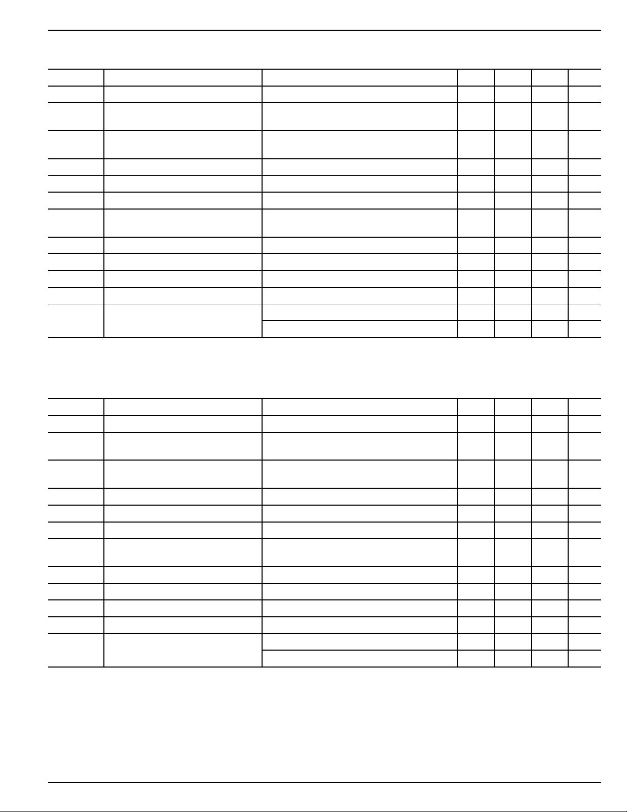
Pin Configuration
IN+
OUTV+
13
2
Part
Identification
Axx
45
IN–
V–
Pin Description
Pin Number Pin Name Pin Function
1 OUT Amplifier Output
2 V+ Positive Supply
3 IN+ Noninverting Input
4 IN– Inverting Input
5 V– Negative Suppy
Functional Configuration
IN+
45
IN–
SOT-23-5 (M5)
OUTV+
2
13
V–
Micrel, Inc. • 1849 Fortune Drive • San Jose, CA 95131 • USA • tel + 1 (408) 944-0800 • fax + 1 (408) 944-0970 • http://www.micrel.com
June 1999 1 MIC7211/7221
Page 2

MIC7211/7221
Micrel
Absolute Maximum Ratings (Note 1)
Supply Voltage (VV+ – VV–)...........................................12V
Differential Input Voltage (V
I/O Pin Voltage (V
IN+
, V
OUT
............................................ VV+ + 0.3V to VV– – 0.3V
Junction Temperature (TJ) ...................................... +150°C
, V
IN+
) .............±(VV+ – VV–)
IN–
), Note 3 ..................................
Operating Ratings (Note 2)
Supply Voltage (VV+ – VV–).............................. 2.2V to 10V
Junction Temperature (TJ) ......................... –40°C to +85°C
Maximum Junction Temperature (T
Package Thermal Resistance (θJA) Note 5 ..........325°C/W
Maximum Power Dissipation.................................... Note 4
) Note 4 . +125°C
J(max)
Storage Temperature (TS) .......................–65°C to +150°C
ESD, Note 6
DC Electrical Characteristics (2.2V)
VV+ = +2.2V, VV– = 0V, VCM = V
Symbol Parameter Condition Min Typ Max Units
V
OS
TCV
TCV
I
B
I
OS
OS
OS
Input Offset Voltage 210mV
Input Offset Voltage 1 µV/°C
Temperature Drift
Input Offset Voltage 3.3
Drift Over Time
Input Bias Current 0.5 pA
Input Offset Current 0.25 pA
CMRR Common-Mode Rejection Ratio 0V ≤ VCM ≤ 2.2V 60 dB
PSRR Positive Power Supply V
Rejection Ratio
A
V
V
I
VOL
OH
OL
S
Gain 125 dB
Output Voltage (High) MIC7211, I
Output Voltage (Low) I
Supply Current V
= VV+/2; TJ = 25°C, bold values indicate –40°C ≤ TJ ≤ +85°C; Note 7; unless noted
OUT
= 2.2V to 5V 90 dB
V+
= 2.5mA 2.1 2.18 V
LOAD
= 2.5mA 0.02 0.1 V
LOAD
= low 5 12 µA
OUT
µV
⁄month
DC Electrical Characteristics (2.7V)
VV+ = +2.7V, VV– = 0V, VCM = V
Symbol Parameter Condition Min Typ Max Units
V
OS
TCV
OS
Input Offset Voltage 210mV
Input Offset Voltage 1 µV/°C
Temperature Drift
TCV
OS
Input Offset Voltage 3.3
Drift Over Time
I
B
I
OS
Input Bias Current 0.5 pA
Input Offset Current 0.25 pA
CMRR Common-Mode Rejection Ratio 0V ≤ VCM ≤ 2.7V 65 dB
PSRR Positive Power Supply V
Rejection Ratio
A
V
V
I
VOL
OH
OL
S
Gain 125 dB
Output Voltage (High) MIC7211, I
Output Voltage (Low) I
Supply Current V
= VV+/2; TJ = 25°C, bold values indicate –40°C ≤ TJ ≤ +85°C; Note 7; unless noted
OUT
= 2.7V to 5V 90 dB
V+
= 2.5mA 2.6 2.68 V
LOAD
= 2.5mA 0.02 0.1 V
LOAD
= low 5 12 µA
OUT
µV
⁄month
MIC7211/7221 2 June 1999
Page 3
MIC7211/7221
Micrel
DC Electrical Characteristics (5V)
VV+ = +5.0V, VV– = 0V, VCM = V
Symbol Parameter Condition Min Typ Max Units
V
OS
TCV
OS
Input Offset Voltage 210mV
Input Offset Voltage 1 µV/°C
Temperature Drift
TCV
OS
Input Offset Voltage 3.3
Drift Over Time
I
B
I
OS
Input Bias Current 0.5 pA
Input Offset Current 0.25 pA
CMRR Common-Mode Rejection Ratio 0V ≤ VCM ≤ 5.0V 70 dB
PSRR Positive Power Supply V
Rejection Ratio
A
V
V
I
I
VOL
OH
OL
S
SC
Gain 125 dB
Output Voltage (High) MIC7211, I
Output Voltage (Low) I
Supply Current V
Short Circuit Current MIC7211, sourcing 150 mA
= VV+/2; TJ = 25°C, bold values indicate –40°C ≤ TJ ≤ +85°C; Note 7; unless noted
OUT
= 5.0V to 10V 90 dB
V+
= 5mA 4.9 4.95 V
LOAD
= 5mA 0.05 0.1 V
LOAD
= low 7 14 µA
OUT
sinking 110 mA
µV
⁄month
DC Electrical Characteristics (10V)
VV+ = +10V, VV– = 0V, VCM = V
Symbol Parameter Condition Min Typ Max Units
V
OS
TCV
TCV
I
B
I
OS
OS
OS
Input Offset Voltage 210mV
Input Offset Voltage 1 µV/°C
Temperature Drift
Input Offset Voltage 3.3
Drift Over Time
Input Bias Current 0.5 pA
Input Offset Current 0.25 pA
CMRR Common-Mode Rejection Ratio 0V ≤ VCM ≤ 10V 75 dB
PSRR Positive Power Supply V
Rejection Ratio
A
V
V
I
I
VOL
OH
OL
S
SC
Gain 125 dB
Output Voltage (High) MIC7211, I
Output Voltage (Low) I
Supply Current V
Short Circuit Current MIC7211, sourcing 165 mA
= VV+/2; TJ = 25°C, bold values indicate –40°C ≤ TJ ≤ +85°C; Note 7; unless noted
OUT
= 5.0V to 10V 90 dB
V+
= 5mA 9.9 9.95 V
LOAD
= 5mA 0.05 0.1 V
LOAD
= low 12 25 µA
OUT
sinking 125 mA
µV
⁄month
June 1999 3 MIC7211/7221
Page 4

MIC7211/7221
V+
V–
OUT
Micrel
AC Electrical Characteristics
VV– = 0V, VCM = V
Symbol Parameter Condition Min Typ Max Units
t
RISE
t
FALL
t
PHL
t
PLH
= VV+/2; TJ = 25°C, bold values indicate –40°C ≤ TJ ≤ +85°C; Note 7; unless noted
OUT
Rise Time VV+ = 5.0V, f = 10kHz, C
= 50pF 75 ns
LOAD
overdrive = 10mV, Note 9
Fall Time VV+ = 5.0V, f = 10kHz, C
= 50pF 70 ns
LOAD
overdrive = 10mV, Note 9
Propagation Delay-High to Low VV+ = 2.2V, f = 10kHz, C
= 50pF 10 µs
LOAD
overdrive = 10mV, Note 9
V
= 2.2V, f = 10kHz, C
V+
= 50pF 6.0 µs
LOAD
overdrive = 100mV, Note 9
V
= 5.0V, f = 10kHz, C
V+
= 50pF 13 µs
LOAD
overdrive = 10mV, Note 9
V
= 5.0V, f = 10kHz, C
V+
overdrive = 100mV, Note 9
Propagation Delay-Low to High VV+ = 2.2V, f = 10kHz, C
overdrive = 10mV, Note 9
= 2.2V, f = 10kHz, C
V
V+
overdrive = 100mV, Note 9
= 5.0V, f = 10kHz, C
V
V+
overdrive = 10mV, Note 9
V
= 5.0V, f = 10kHz, C
V+
= 50pF 5 µs
LOAD
= 50pF 13.5 µs
LOAD
= 50pF 4.0 µs
LOAD
= 50pF 11.5 µs
LOAD
= 50pF 3.0 µs
LOAD
overdrive = 100mV, Note 9
Note 1. Exceeding the absolute maximum rating may damage the device.
Note 2. The device is not guaranteed to function outside its operating rating.
Note 3. I/O pin voltage is any external voltage to which an input or output is referenced.
Note 4. The maximum allowable power dissipation is a function of the maximum junction temperature, T
Note 5. Thermal resistance, θJA, applies to a part soldered on a printed circuit board.
Note 6. Devices are ESD sensitive. Handling precautions recommended.
Note 7. All limits guaranteed by testing on statistical analysis.
Note 8. Continuous short circuit may exceed absolute maximum TJ under some conditions.
Note 9. The MIC7221 requires 5kΩ pull-up resistor.
resistance, θJA; and the ambient temperature, TA. The maximum allowable power dissipation at any ambient temperature is calculated using
P
D(max)
= (T
– TA) ÷ θJA. Exceeding the maximum allowable power dissipation will result in excessive die temperature.
J(max)
Partial Functional Diagrams
V+
OUT
V–
; the junction-to-ambient thermal
J(max)
MIC7211 Push-Pull Output
MIC7221 Open-Drain Output
MIC7211/7221 4 June 1999
Page 5

MIC7211/7221
V
+
R
IN
V
IN
(>>V+)
V
REF
R1
R
F
V
OUT
0.1µF
Note: 1V ≤ V++ ≤ 10V
V
++
R
PU
POSSIBLE
DISCONNECT
0V WHEN
SUPPLY
IS OFF
Power
Supply
Output
Micrel
Application Information
The small outline and low supply current (typically 7µA at 5V)
of the MIC7211/21 are the primary advantages of these
comparators. They have been characterized for 2.2V, 2.7V,
5V, and 10V operation.
Their 2.2V capability is especially useful in low-battery voltage situations. Low-voltage operation allows longer battery
life or deeper discharge capability. Even at 2.2V, the output
can drive several logic-gate inputs. At 2.5mA, the output
stage voltage drop is guaranteed to not exceed 0.1V.
Outputs
The MIC7211 has a push-pull output while the MIC7221 has
an open-drain output, otherwise both comparators share a
common design.
The open-drain MIC7221 output can be pulled up to 10V,
even when the supply voltage is as low as 2.2V. Conversely,
the output also can be pulled up to voltages that are lower
than the positive supply. Logic-level translation is readily
facilitated by the ability to pull the open-drain output to
voltages above or below the power supply.
Although specified short-circuit output current specified for
these parts typically exceeds 100mA, their output is not
intended to sink or source anywhere near 100mA. The shortcircuit rating is only presented as additional information
regarding output impedance and may be useful for determining the voltage drop one may experience when driving a given
load.
Input Bias Current
The low input-bias current (typically 0.5pA) requirement of
the MIC7211/21 provides flexibility in the kinds of circuitry and
devices that can be directly interfaced.
Designs using an amplifier for transducer-to-comparator
impedance transformation may be simplified by using the
MIC7211/21’s low-input-current requirement to eliminate the
amplifier.
Input Signal Levels
Input signals may exceed either supply rail by up to 0.2V
without phase inversion or other adverse effects. The inputs
have internal clamp diodes to the supply pins.
+
V
R
0.1µF
V
F
OUT
R
V
(±100V)
V
REF
Note: RF and R1 control hysteresis (typically, RF >> R1).
Figure 1. Driving the Input Beyond the Supply Rails
Larger input swings can be accommodated if the input current
is limited to 1mA or less. Using a 100k input resistor will allow
an input to swing up to 100V beyond either supply rail.
Because of the low input bias current of the device, even
IN
IN
≥100k
R1
larger input resistors are practical. See Figure 1. The ability
to swing the input beyond either rail facilitates some otherwise difficult circuits, such as a single-supply zero-crossing
detector or a circuit that senses its own supply voltage.
The comparator must be powered if an input is pulled above
the rail, even with current limiting in effect. Figure 2 shows a
hypothetical situation where an input is pulled higher than the
rail when the power supply is off or not present. Figure 2 also
shows external clamp diodes for additional input circuit
protection. Discrete clamp diodes can be arbitrarily more
robust than the internal clamp diodes.
The power supply has been simplified (real power supplies do
not have a series output diode); however, this illustrates a
common characteristic of most positive-voltage power supplies: they are designed to source, but not sink, current. If the
supply is off, or disconnected, there is no limiting voltage for
the clamp diode to reference. The input signal can charge the
the bypass capacitor, and possibly the filter capacitor, up to
the applied input (VIN). This may be high enough to cause a
thin-oxide rupture in a CMOS integrated circuit.
Figure 2. Avoid This Condition
Ideally, the supply for the comparator and the input-producing circuitry should the same or be switched simultaneously.
Bypass Capacitors
CMOS circuits, especially logic gates with their totem-pole
(push-pull) output stages, generate power supply current
spikes (noise) on the supply and/or ground lines. These
spikes occur because, for a finite time during switching, both
output transistors are partially on allowing “shoot-through
current.” Bypass capacitors reduce this noise.
Adequate bypassing for the MIC7211 comparator is 0.01µF;
in low-noise systems, where this noise may interfere with the
functioning or accuracy of nearby circuitry, 0.1µF is recommended. Because the MIC7221 does not have a totem-pole
output stage, this spiking is not evident; however, switching
a capacitive load can present a similar situation.
Thermal Behavior
The thermal impedance of a SOT-23-5 package is 325˚C/W.
The 5V Electrical Characteristics table shows a maximum
voltage drop of 0.1V for a 5mA output current, making the
output resistance about 20Ω (R = 0.1/0.005 = 20Ω). Attempting to draw the typical specified output short-circuit current of
150mA (sourcing) can be expected to cause a die temperature
rise
of 146˚C. (Operating die temperature for ICs should
generally not exceed 125˚C.) Using a series resistance is the
simplest form of protecting against damage by excessive
output current.
June 1999 5 MIC7211/7221
Page 6

MIC7211/7221
Package Information
1.90 (0.075) REF
0.95 (0.037) REF
Micrel
3.02 (0.119)
2.80 (0.110)
0.50 (0.020)
0.35 (0.014)
1.75 (0.069)
1.50 (0.059)
1.30 (0.051)
0.90 (0.035)
0.15 (0.006)
0.00 (0.000)
SOT-23-5 (M5)
3.00 (0.118)
2.60 (0.102)
10°
0°
DIMENSIONS:
MM (INCH)
0.20 (0.008)
0.09 (0.004)
0.60 (0.024)
0.10 (0.004)
MIC7211/7221 6 June 1999
Page 7

MIC7211/7221
Micrel
June 1999 7 MIC7211/7221
Page 8

MIC7211/7221
Micrel
MICREL INC. 1849 FORTUNE DRIVE SAN JOSE, CA 95131 USA
TEL + 1 (408) 944-0800 FAX + 1 (408) 944-0970 WEB http://www.micrel.com
This information is believed to be accurate and reliable, however no responsibility is assumed by Micrel for its use nor for any infringement of patents or
other rights of third parties resulting from its use. No license is granted by implication or otherwise under any patent or patent right of Micrel Inc.
© 1999 Micrel Incorporated
MIC7211/7221 8 June 1999
 Loading...