

Page 1
MIC7122 MicrelMIC7122 Micrel
MIC7122
Rail-to-Rail Dual Op Amp
Preliminary Information
General Description
The MIC7122 is a dual high-performance CMOS operational
amplifier featuring rail-to-rail inputs and outputs.
The input common-mode range extends beyond the rails by
300mV, and the output voltage swings to within 150µV of both
rails when driving a 100kΩ load.
The amplifiers operate from 2.2V to 15V and are fully specified at 2.2V, 5V, and 15V. Gain bandwidth and slew rate are
750kHz and 0.7V/µs, respectively at 2.2V supply.
The MIC7122 is available in the MM8™ 8-lead MSOP package.
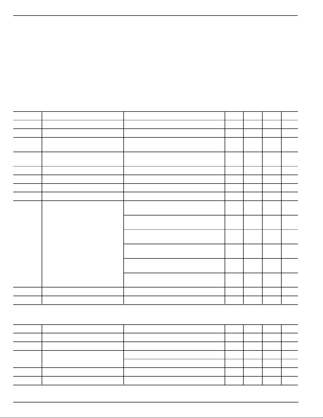
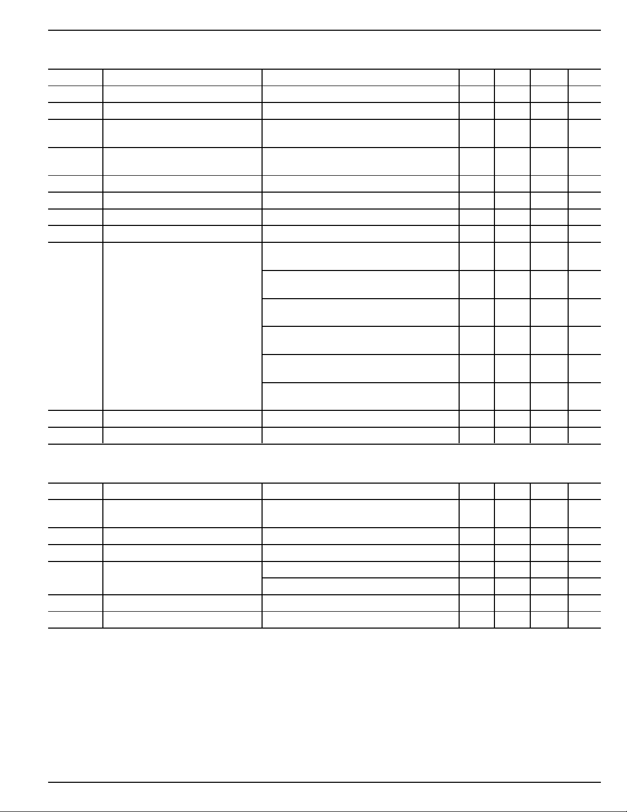
Pin Configuration
Features
• Small footprint MSOP-8 package
• 350µA supply current per op amp at 2.2V supply
• Guaranteed 2.2V, 5V, and 15V performance
• 750kHz gain-bandwidth product at 2.2V supply
• 0.01% total harmonic distortion at 1kHz (15V, 2kΩ)
• Drives 200pF at 5V and greater supply voltages
Applications
• Battery-powered instrumentation
• PCMCIA, USB peripherals
• Portable computers and PDAs
Ordering Information
Part Number Temperature Range Package
MIC7122BMM –40°C to +85°C MSOP-8
OUT A
IN A–
IN A+
V–
1
2
3
4
8
7
6
5
V+
OUT B
INB–
INB+
MSOP-8 (MM)
Pin Description
Pin Number Pin Name Pin Function
1 / 7 OUTA / OUTB Amplifier Outputs
2 / 6 INA– / INB– Inverting Inputs
3 / 5 INA+ / INB+ Noninverting Inputs
4 V– Negative Supply: Negative supply for split supply application or ground for
8 V+ Positive Supply
single supply applications.
1
2
A
3
4
8
7
6
B
5
MM8 is a trademark of Micrel, Inc.
Micrel, Inc. • 1849 Fortune Drive • San Jose, CA 95131 • USA • tel + 1 (408) 944-0800 • fax + 1 (408) 944-0970 • http://www.micrel.com
March 1999 1 MIC7122
Page 2
MIC7122 Micrel
Absolute Maximum Ratings (Note 1)
Supply Voltage (VV+ – VV–)........................................16.5V
Differential Input Voltage (V
I/O Pin Voltage (VIN, V
OUT
.............................................V
Junction Temperature (TJ) ...................................... +150°C
Storage Temperature ...............................–65°C to +150°C
– V
IN+
), Note 3
) .......................±10V
IN–
+ 0.3V to V
V+
V–
– 0.3V
Operating Ratings (Note 2)
Supply Voltage (VV+ – VV–).............................. 2.2V to 15V
Junction Temperature (TJ) ......................... –40°C to +85°C
Max. Junction Temperature (T
Max. Power Dissipation............................................ Note 4
Package Thermal Resistance, Note 5
MSOP-8 (θJA)....................................................200°C/W
), Note 4 .........+125°C
J(max)
Lead Temperature (soldering, 10 sec.) .....................260°C
ESD, Note 6..............................................................1000V
DC Electrical Characteristics (2.2V)
VV+ = +2.2V, VV– = 0V, VCM = V
Symbol Parameter Condition Min Typ Max Units
V
OS
TCV
I
B
I
OS
R
IN
OS
Input Offset Voltage 0.5 9 mV
Input Offset Voltage Average Drift 3.0 µV/°C
Input Bias Current 1.0 10 pA
Input Offset Current 0.5 5 pA
Input Resistance >1 TΩ
CMRR Common-Mode Rejection Ratio -0.3V ≤ VCM ≤ 2.5V, Note 9 45 65 dB
±PSRR Power Supply Rejection Ratio VV+ = VV– = 1.1V to 2.5V, V
C
IN
V
O
I
SC
I
S
Common-Mode Input Capacitance 3 pF
Output Swing output high, RL = 100k, 0.15 1 mV
Output Short Circuit Current sinking or sourcing, Note 8 20 50 mA
Supply Current both amplifiers 0.7 1.6 mA
= VV+/2; RL = 1MΩ; TJ = 25°C, bold values indicate –40°C ≤ TJ ≤ +85°C
OUT
= VCM = 0 60 85 dB
OUT
specified as VV+ – V
output low, R
output high, R
specified as VV+ – V
output low, R
output high, R
specified as VV+ – V
output low, R
OUT
= 100k 0.15 1 mV
L
= 2k 8 33 mV
L
OUT
= 2k 8 33 mV
L
= 600Ω 26 110 mV
L
OUT
= 600Ω 26 110 mV
L
; Note 7
; unless noted
64 500 pA
32 250 pA
1 mV
1 mV
50 mV
50 mV
165 mV
165 mV
AC Electrical Characteristics (2.2V)
VV+ = 2.2V, VV– = 0V, VCM = V
Symbol Parameter Condition Min Typ Max Units
SR Slew Rate 0.7 V/µs
GBW Gain-Bandwidth Product 750 kHz
φ
m
G
m
Phase Margin CL = 0pF 80 °
Gain Margin 10 dB
Interamplifier Isolation Note 12 90 dB
MIC7122 2 March 1999
= VV+/2; RL = 1MΩ; TJ = 25°C, bold values indicate –40°C ≤ TJ ≤ +85°C
OUT
CL = 200pF 40 °
; Note 7
; unless noted
Page 3
MIC7122 Micrel
DC Electrical Characteristics (5V)
VV+ = +5.0V, VV– = 0V, VCM = 1.5V, V
Symbol Parameter Condition Min Typ Max Units
V
OS
TCV
I
B
I
OS
R
IN
OS
Input Offset Voltage 0.5 9 mV
Input Offset Voltage Average Drift 3.0 µV/°C
Input Bias Current 1.0 10 pA
Input Offset Current 0.5 5 pA
Input Resistance >1 TΩ
CMRR Common-Mode Rejection Ratio -0.3V ≤ VCM ≤ 5.3V, Note 9 55 75 dB
±PSRR Power Supply Rejection Ratio VV+ = VV– = 2.5V to 7.5V, V
C
V
I
I
IN
OUT
SC
S
Common-Mode Input Capacitance 3 pF
Output Swing output high, RL = 100k 0.3 1.0 mV
Output Short Circuit Current sinking or sourcing, Note 8 40 140 mA
Supply Current both amplifiers 0.8 1.8 mA
= VV+/2; RL = 1MΩ; TJ = 25°C, bold values indicate –40°C ≤ TJ ≤ +85°C; Note 7; unless noted
OUT
64 500 pA
32 250 pA
= VCM = 0 55 100 dB
OUT
specified as VV+ – V
output low, R
= 100k 0.3 1.0 mV
L
OUT
1.5 mV
1.5 mV
output high, R
specified as VV+ – V
output low, R
= 2k 13 50 mV
L
OUT
= 2k 13 50 mV
L
75 mV
75 mV
output high, R
specified as VV+ – V
output low, R
= 600Ω 40 165 mV
L
OUT
= 600Ω 40 165 mV
L
250 mV
250 mV
AC Electrical Characteristics (5V)
VV+ = 5V, VV– = 0V, VCM = 1.5V, V
Symbol Parameter Condition Min Typ Max Units
THD Total Harmonic Distortion f = 1kHz, A
SR Slew Rate 0.6 V/µs
GBW Gain-Bandwidth Product 465 kHz
φ
m
G
m
Phase Margin CL = 0pF 85 °
Gain Margin 10 dB
Interamplifier Isolation Note 12 90 dB
= VV+/2; RL = 1MΩ; TJ = 25°C, bold values indicate –40°C ≤ TJ ≤ +85°C
OUT
= –2, 0.05 %
RL = 2kΩ, V
V
OUT
= 4.0 V
PP
CL = 200pF 40 °
; Note 7
; unless noted
March 1999 3 MIC7122
Page 4
MIC7122 Micrel
DC Electrical Characteristics (15V)
VV+ = +15V, VV– = 0V, VCM = 1.5V, V
Symbol Parameter Condition Min Typ Max Units
V
OS
TCV
I
B
I
OS
R
IN
OS
Input Offset Voltage 0.5 9 mV
Input Offset Voltage Average Drift 3.0 µV/°C
Input Bias Current 1.0 10 pA
Input Offset Current 0.5 5 pA
Input Resistance >1 TΩ
CMRR Common-Mode Rejection Ratio -0.3V ≤ VCM ≤ 15.3V, Note 9 60 85 dB
±PSRR Power Supply Rejection Ratio VV+ = VV– = 2.5V to 7.5V, V
A
C
V
I
I
V
IN
OUT
SC
S
Large Signal Voltage Gain sourcing or sinking, 340 V/mV
Common-Mode Input Capacitance 3 pF
Output Swing output high, RL = 100k 0.8 2 mV
Output Short Circuit Current sinking or sourcing, Notes 8 50 250 mA
Supply Current both amplifiers 0.9 2.0 mA
= VV+/2; RL = 1MΩ; TJ = 25°C, bold values indicate –40°C ≤ TJ ≤ +85°C; Note 7; unless noted
OUT
64 500 pA
32 250 pA
= VCM = 0 55 100 dB
OUT
RL = 2k, Note 10
sourcing or sinking, 300 V/mV
RL = 600Ω, Note 10
specified as VV+ – V
output low, R
= 100k 0.8 2 mV
L
OUT
3 mV
3 mV
output high, R
specified as VV+ – V
output low, R
output high, R
specified as VV+ – V
output low, R
= 2k 40 80 mV
L
OUT
= 2k 40 80 mV
L
= 600Ω 130 270 mV
L
OUT
= 600Ω 130 270 mV
L
120 mV
120 mV
400 mV
400 mV
AC Electrical Characteristics (15V)
VV+ = 15V, VV– = 0V, VCM = 1.5V, V
Symbol Parameter Condition Min Typ Max Units
THD Total Harmonic Distortion f = 1kHz, A
SR Slew Rate V+ = 15V, Note 11 0.5 V/µs
GBW Gain-Bandwidth Product 420 kHz
φ
m
G
m
e
n
i
n
Phase Margin CL = 0pF 85 °
Gain Margin 10 dB
Input-Referred Voltage Noise f = 1kHz, VCM = 1V 37
Input-Referred Current Noise f = 1kHz 1.5
Interamplifier Isolation Note 12 90 dB
MIC7122 4 March 1999
= VV+/2; RL = 1MΩ; TJ = 25°C, bold values indicate –40°C ≤ TJ ≤ +85°C
OUT
= –2, 0.01 %
RL = 2k, V
V
OUT
= 8.5 V
PP
CL = 500pF 40 °
; Note 7
; unless noted
nV/ Hz
fA/ Hz
Page 5

MIC7122 Micrel
Note 1. Exceeding the absolute maximum rating may damage the device.
Note 2. The device is not guaranteed to function outside its operating rating.
Note 3. I/O Pin Voltage is any external voltage to which an input or output is referenced.
Note 4. The maximum allowable power dissipation is a function of the maximum junction temperature, T
resistance, θJA; and the ambient temperature, TA. The maximum allowable power dissipation at any ambient temperature is calculated using:
PD = (T
– TA) ÷ θJA. Exceeding the maximum allowable power dissipation will result in excessive die temperature.
J(max)
Note 5. Thermal resistance, θJA, applies to a part soldered on a printed-circuit board.
Note 6. Devices are ESD protected; however, handling precautions are recommended. Human body model, 1.5kΩ in series with 100pF.
Note 7. All limits guaranteed by testing or statistical analysis.
Note 8. Continuous short circuit may exceed absolute maximum TJ under some conditions.
Note 9. CMRR is determined as follows: The maximum ∆VOS over the VCM range is divided by the magnitude of the VCM range. The measurement
points are: VCM = V
Note 10. RL connected to 7.5V. Sourcing: 7.5V ≤ V
– 0.3V, (VV+ – VV–)/2, and V
V–
OUT
+ 0.3V.
V+
≤ 12.5V. Sinking: 2.5V ≤ V
OUT
≤ 7.5V.
Note 11. Device connected as a voltage follower with a 10V step input. The value is the positive or negative slew rate, whichever is slower.
Note 12. Referenced to input.
; the junction-to-ambient thermal
J(max)
March 1999 5 MIC7122
Page 6
MIC7122 Micrel
Application Information
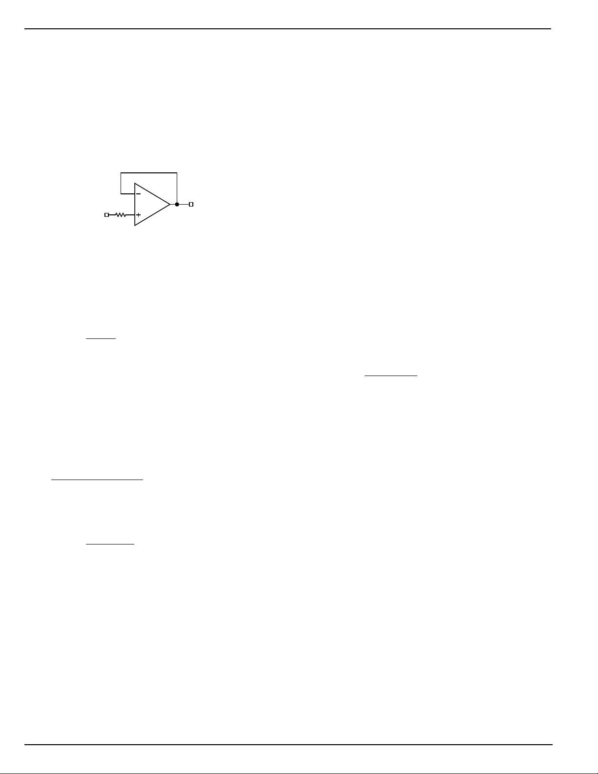
Input Common-Mode Voltage
The MIC7122 tolerates input overdrive by at least 300mV
beyond either rail without producing phase inversion.
If the absolute maximum input voltage is exceeded, the input
current should be limited to ±5mA maximum to prevent
reducing reliability. A 10kΩ series input resistor, used as a
current limiter, will protect the input structure from voltages as
large as 50V above the supply or below ground. See Figure
1.
V
R
IN
V
IN
10kΩ
Figure 1. Input Current-Limit Protection
Output Voltage Swing
Sink and source output resistances of the MIC7122 are
equal. Maximum output voltage swing is determined by the
load and the approximate output resistance. The output
resistance is:
V
=
I
LOAD
and I
DROP
can be determined from the V
LOAD
R
OUT
V
is the voltage dropped within the amplifier output
DROP
stage. V
DROP
(output swing) portion of the appropriate Electrical Characteristics table. I
minus V+/2 and divided by R
is equal to the typical output high voltage
LOAD
LOAD
Electrical Characteristics DC (5V) table, the typical output
high voltage drops 13mV using a 2kΩ load (connected to V+/
2), which produces an I
5.0V – 0.013V – 2.5V
2k
Ω
LOAD
of:
1.244mA
=
Because of output stage symmetry, the corresponding typical
output low voltage (13mV) also equals V
R
OUT
0.013V
==10 5. Ω
0.001244A
Power Dissipation
The MIC7122 output drive capability requires considering
power dissipation. If the load impedance is low, it is possible
to damage the device by exceeding the 125°C junction
temperature rating.
On-chip power consists of two components: supply power
and output stage power. Supply power (PS) is the product of
the supply voltage (VS = VV+ – VV–) and supply current (IS).
Output stage power (PO) is the product of the output stage
OUT
. For example, using the
. Then:
DROP
voltage drop (V
) and the output (load) current (I
DROP
Total on-chip power dissipation is:
PD = PS + P
PD = VSIS + V
O
DROPIOUT
where:
PD = total on-chip power
PS = supply power dissipation
PO = output power dissipation
VS = VV+ – V
V–
IS = power supply current
V
DROP
V
DROP
= VV+ – V
= V
OUT
– V
OUT
V–
(sourcing current)
(sinking current)
The above addresses only steady state (dc) conditions. For
non-dc conditions the user must estimate power dissipation
based on rms value of the signal.
The task is one of determining the allowable on-chip power
dissipation for operation at a given ambient temperature and
power supply voltage. From this determination, one may
calculate the maximum allowable power dissipation and,
after subtracting PS, determine the maximum allowable load
current, which in turn can be used to determine the miniumum
load impedance that may safely be driven. The calculation is
summarized below.
O
P
θ
JA(MSOP-8)
D(max)
=
TT
−
J(max) A
θ
JA
= 200°C/W
Driving Capacitive Loads
Driving a capacitive load introduces phase-lag into the output
signal, and this in turn reduces op-amp system phase margin.
The application that is least forgiving of reduced phase
margin is a unity gain amplifier. The MIC7122 can typically
drive a 200pF capacitive load connected directly to the output
when configured as a unity-gain amplifier and powered with
a 2.2V supply. At 15V operation the circuit typically drives
500pF.
Using Large-Value Feedback Resistors
A large-value feedback resistor (> 500kΩ) can reduce the
phase margin of a system. This occurs when the feedback
resistor acts in conjunction with input capacitance to create
phase lag in the feedback signal. Input capacitance is usually
a combination of input circuit components and other parasitic
capacitance, such as amplifier input capacitance and stray
printed circuit board capacitance.
Figure 2 illustrates a method of compensating phase lag
caused by using a large-value feedback resistor. Feedback
capacitor CFB introduces sufficient phase lead to overcome
the phase lag caused by feedback resistor RFB and input
OUT
).
MIC7122 6 March 1999
Page 7

MIC7122 Micrel
C
capacitance CIN. The value of CFB is determined by first
estimating CIN and then applying the following formula:
RIN × CIN ≤ RFB × C
R
V
IN
C
FB
C
FB
R
FB
IN
V
OUT
IN
Figure 2. Cancelling Feedback Phase Lag
Since a significant percentage of CIN may be caused by board
layout, it is important to note that the correct value of CFB may
change when changing from a breadboard to the final circuit
layout.
Typical Circuits
Some single-supply, rail-to-rail applications for which the
MIC7122 is well suited are shown in the circuit diagrams of
V
IN
0V to V+
Figure 4. Voltage Follower/Buffer
V+
V
IN
0V to 2V
Change Q1 and R
for higher current
and/or different gain.
V
I
==
OUT
R
V+
1
V
0.5V to Q1 V
1
⁄2 MIC7122
S
IN
100mA/V as shown
S
⁄2 MIC7122
V
OUT
S
CEO(sus)
0V to V+
Load
I
OUT
Q1
2N3904
R
S
10Ω
1
⁄2W
V
OUT
0V to V+
= V
IN
V
OUT
V
CEO
{
I
C(max)
= 40V
= 200mA
Figures 3 through 7.
V+
1
⁄2 MIC7122
V
OUT
0V to V+
0V to
V
IN
V+
A
V
R2
910k
R1
100k
Figure 3a. Noninverting Amplifier
Figure 5. Voltage-Controlled Current Sink
R4
R3
100k
100k
V+
1
R4
100k
⁄2 MIC7122
V
OUT
V+
0V
C1
0.001µF
V+
R2
100k
100
V+
(V)
OUT
V
0
0 100
A1
=+ ≈10
V
VIN (V)
R2
R1
Figure 3b. Noninverting Amplifier Behavior
Figure 6. Square Wave Oscillator
IN
V+
R1
33k
R3
330k
C1
1µF
R2
330k
V+
1
⁄2 MIC7122
A
R4
330k
C
OUT
V
OUT
0V
R
L
R2R1330k
=− = =−
V
33k
10
Figure 7. AC-Coupled Inverting Amplifier
March 1999 7 MIC7122
Page 8

MIC7122 Micrel
Package Information
0.122 (3.10)
0.112 (2.84)
0.036 (0.90)
0.032 (0.81)
0.012 (0.03)
0.0256 (0.65) TYP
0.199 (5.05)
0.187 (4.74)
0.120 (3.05)
0.116 (2.95)
0.043 (1.09)
0.038 (0.97)
0.012 (0.30) R
0.008 (0.20)
0.004 (0.10)
5° MAX
0° MIN
MM8™ 8-Lead MSOP (MM)
DIMENSIONS:
INCH (MM)
0.007 (0.18)
0.005 (0.13)
0.012 (0.03) R
0.039 (0.99)
0.035 (0.89)
0.021 (0.53)
MICREL INC. 1849 FORTUNE DRIVE SAN JOSE, CA 95131 USA
TEL + 1 (408) 944-0800 FAX + 1 (408) 944-0970 WEB http://www.micrel.com
This information is believed to be accurate and reliable, however no responsibility is assumed by Micrel for its use nor for any infringement of patents or
other rights of third parties resulting from its use. No license is granted by implication or otherwise under any patent or patent right of Micrel Inc.
© 1999 Micrel Incorporated
MIC7122 8 March 1999
 Loading...