

Page 1
MIC6251/6252 Micrel
MIC6251/6252
IttyBitty™ GainBlock™ Amplifiers
Preliminary Information
General Description
The MIC6251 and MIC6252 are IttyBitty™ GainBlock™
amplifiers for use as follows:
MIC6251................................ +2, +1, –1 gain amplifier
MIC6252.................................. +0.5, +1 gain amplifier;
average value amplifier
The MIC6251 and MIC6252 amplifiers operate from 4V to
32V. Both can use single or split supplies. These amplifiers
feature internal, well-matched, gain-setting resistors and an
input common-mode range that includes the negative supply
(ground).
The MIC6251/2 is available in the tiny SOT-23-5 surface
mount package.
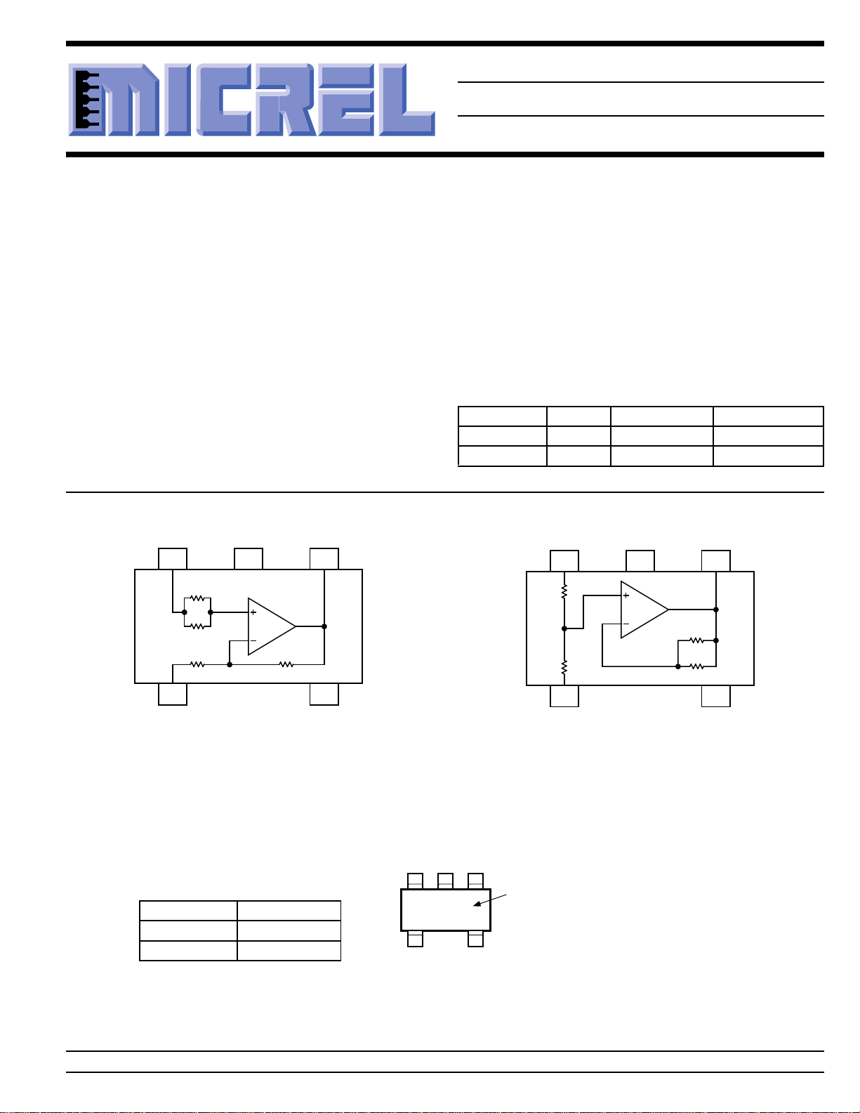
Functional Configuration
IN+
321
V– OUT
Features
• 4V to 32V operation
• Small footprint package
• Internally compensated
• 2MHz bandwidth
• 6V/µs typical slew rate
• Short circuit protected
Applications
• Analog building blocks
• Summing amplifier
• Gain block
Ordering Information
Part Number Marking Temperature Range Package
MIC6251BM5 A51 –40°C to +85°C SOT-23-5
MIC6252BM5 A52 –40°C to +85°C SOT-23-5
IN+ V– OUT
321
20k
20k
4 5
IN– V+
Pin Configuration
Part Number Identification
MIC6251BM5 A51
MIC6252BM5 A52
MIC6251
20k
20k
20k20k
20k
4 5
IN– V+
20k
MIC6252
V–
2
Axx
OUT
13
Part
Identification
V+IN–
IN+
45
SOT-23-5 (M5)
IttyBitty and GainBlock are a trademarks of Micrel, Inc.
Micrel, Inc. • 1849 Fortune Drive • San Jose, CA 95131 • USA • tel + 1 (408) 944-0800 • fax + 1 (408) 944-0970 • http://www.micrel.com
July 1998 1 MIC6251/6252
Page 2
MIC6251/6252 Micrel
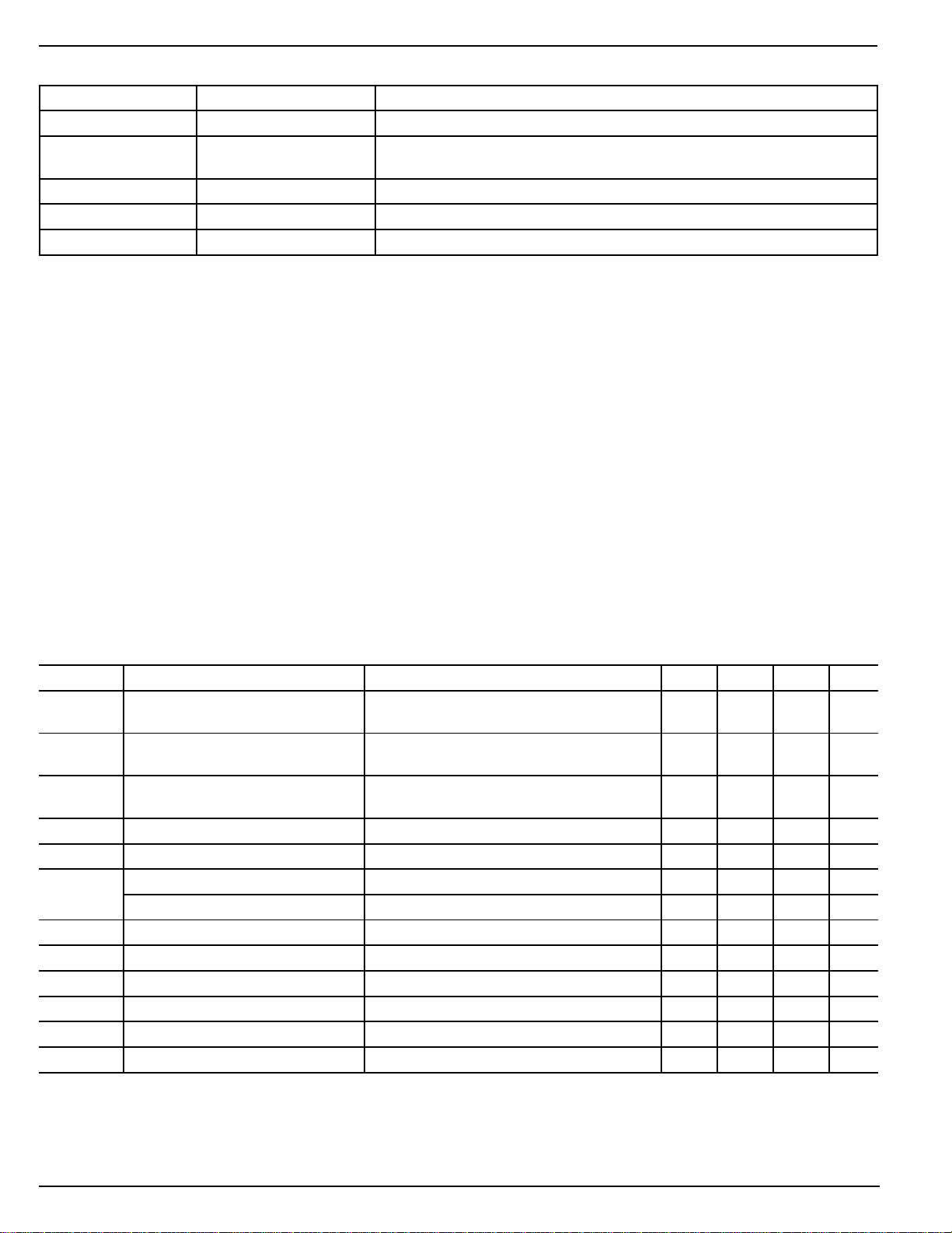
Pin Description
Pin Number Pin Name Pin Function
1 OUT Amplifier Output
2 V– Negative Supply: Negative supply for split supply application or ground for
single supply application.
3 IN+ Noninverting Input: See “Electrical Characteristics: Note 1.”
4 IN– Inverting Input: See “Electrical Characteristics: Note 1.”
5 V+ Positive Supply
Absolute Maximum Ratings
Supply Voltage (VV+ – VV–)............................. 36V or ±18V
Differential Input Voltage (V
Input Voltage (V
IN+
, V
IN–
IN+
– V
) .......................±36V
IN–
)........................VV– – 0.3V to V
Operating Ratings
Supply Voltage .................................................... 4V to 32V
Ambient Temperature Range..................... –40°C to +85°C
SOT-23-5 Thermal Resistance (θJA).....................325°C/W
V+
Output Short Circuit Current Duration ...............................∞
Junction Temperature (TJ) ........................................ 150°C
Storage Temperature (TS) ....................... –65°C to +150°C
Lead Temperature (soldering, 10 sec.) ..................... 260°C
ESD, Note 4............................................................... [TBD]
Electrical Characteristics (Differential Supply)
VV+ = +15V, VV– = –15V; VCM = 0V, Note 1; TA = 25°C, bold values indicate –40°C ≤ TA ≤ +85°C, TA = TJ; unless noted.
Symbol Parameter Condition Min Typ Max Units
G
E
G
NL
V
OS
TCV
OS
I
B
V
CM
CMRR Common Mode Rejection Ratio ∆VCM = 27V, –13.5V to +13.5V 65 100 dB
PSRR Power Supply Rejection Ratio ∆VS = 25V, ±15V to ±2.5V 65 110 dB
V
OUT
B
W
S
R
I
S
General Note : Devices are ESD protected; however, handling precautions are recommended.
Note 1: IN+ and IN– pins on the MIC6252 are interchangeable.
Note 2: Gain setting resistors are ratio-matched but have a ±20% absolute tolerance
Note 3: Limit input current to 1mA.
Note 4: Human body model, 1.5k in series with 100pF.
Gain Error MIC6251: AV = 2, VO = ±10V 0.3 0.5 %
MIC6252: AV = 0.5, VO = ±10V 0.3 0.5 %
Gain Non-linearity MIC6251: AV = 2, VO = ±10V 0.01 %
MIC6252: AV = 0.5, VO = ±10V 0.01 %
Offset Voltage MIC6251: Referred to output 4 14 mV
MIC6252: Referred to output 2 7 mV
Average Offset Drift 7 µV/°C
Input Bias Current 50 250 nA
Input Voltage Range, Differential Note 3 ±25 V
Input Volt. Range, Common Mode ±13.5 ±13.8 V
Maximum Output Voltage Swing RL = 2k ±12.5 ±14 V
Bandwidth 2 MHz
Slew Rate 6V/µs
Supply Current 1.3 2.0 mA
MIC6251/6252 2 July 1998
Page 3
MIC6251/6252 Micrel
20
30
40
50
60
70
-40 -20 0 20 40 60 80 100
INPUT BIAS CURRENT (nA)
TEMPERATURE (°C)
0
5
10
15
20
25
30
10 100 1000 3000
PEAK-TO-PEAK OUTPUT VOLTAGE (V)
FREQUENCY (kHz)
50
60
70
80
90
100
110
0.01 0.1 1 10 100 1000
CMRR (dB)
FREQUENCY (kHz)
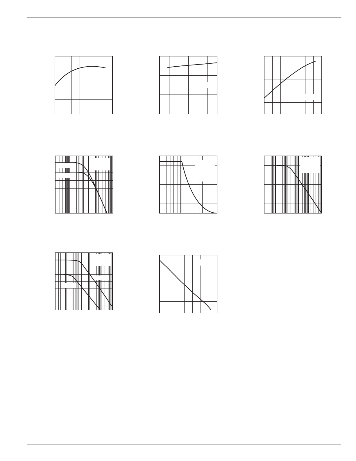
Typical Characteristics
Supply Current
1.4
1.3
1.2
1.1
SUPPLY CURRENT (mA)
1.0
vs. Temperature
VS = ±15V
-40 -20 0 20 40 60 80 100
TEMPERATURE (°C)
MIC6251 Gain
10
-5
-10
GAIN (dB)
-15
-20
-25
vs. Frequency
5
G = +2
0
G = +1
0.01 0.1 1 10 100
FREQUENCY (MHz)
VS = ±15V
= 25°C
T
A
Supply Current
vs. Supply Voltage
1.5
1.0
TA = 25°C
0.5
SUPPLY CURRENT (mA)
0
0 5 10 15 20 25 30
SUPPLY VOLTAGE (V)
Undistorted Output Swing vs.
Frequency
VS = ±15V
= 2k
R
L
G = +2
= 25°C
T
A
Input Bias Current
vs. Temperature
VS = ±15V
Common-Mode Rejection Ratio
vs. Frequency
VS = ±15V
G = +2
= 25°C
T
A
Power Supply Rejection Ratio
130
120
110
100
PSRR (dB)
July 1998 3 MIC6251/6252
vs. Frequency
90
-PSRR
80
70
60
50
0.001 0.01 0.1 1 10 100
FREQUENCY (kHz)
VS = ±15V
T
= 25°C
A
+PSRR
Short Circuit Current
vs. Temperature
65
60
55
50
45
SHORT CIRCUIT CURRENT (mA)
40
-40 -20 0 20 40 60 80 100
TEMPERATURE (°C)
VS = ±15V
Page 4
MIC6251/6252 Micrel
+10V
GND
–10V
+10V
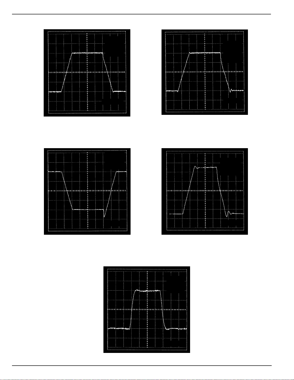
MIC6251 Large-Signal Transient Response
VS = ±15V
= 2k
R
L
C
= 10pF
L
G = +2
2µs/DIV
MIC6251 Large-Signal Transient Response
VS = ±15V
R
= 2k
L
C
= 10pF
L
G = –1
+10V
GND
–10V
+5V
MIC6251 Large-Signal Transient Response
VS = ±15V
R
= 2k
L
= 10pF
C
L
G = +1
2µs/DIV
MIC6252 Large-Signal Transient Response
VS = ±15V
= 2k
R
L
C
= 10pF
L
G = 0.5
GND
–10V
+100mV
GND
–100mV
GND
–5V
2µs/DIV
MIC6251 Small-Signal Transient Response
VS = ±15V
R
= 2k
L
= 100pF
C
L
G = +2
2µs/DIV
500ns/DIV
MIC6251/6252 4 July 1998
Page 5
MIC6251/6252 Micrel
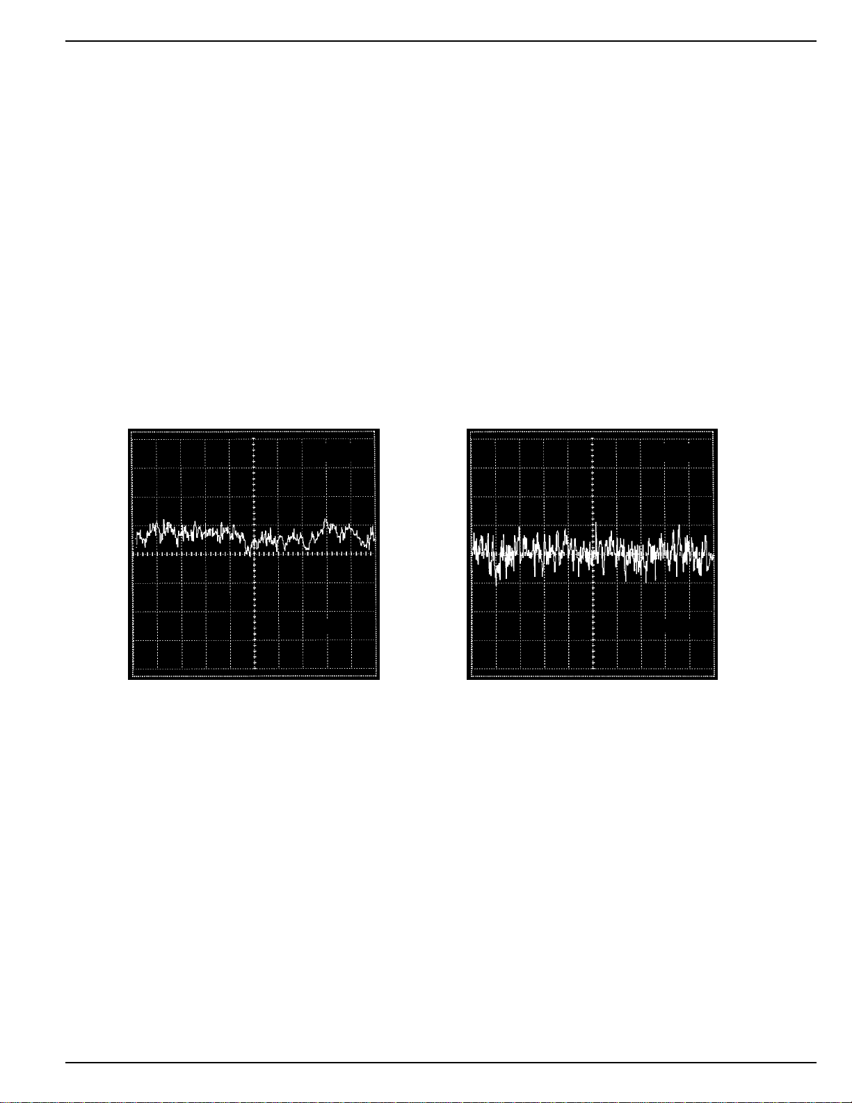
NOISE VOLTAGE (4µV/DIV)
MIC6251/2 0.1Hz to 10Hz Noise
Gain = +1
VS = ±15V
1s/DIV
MIC6251/2 Wideband Noise
Gain +1
VS = ±15V
NOISE VOLTAGE (5µV/DIV)
5ms/DIV
July 1998 5 MIC6251/6252
Page 6
MIC6251/6252 Micrel
Functional Configurations
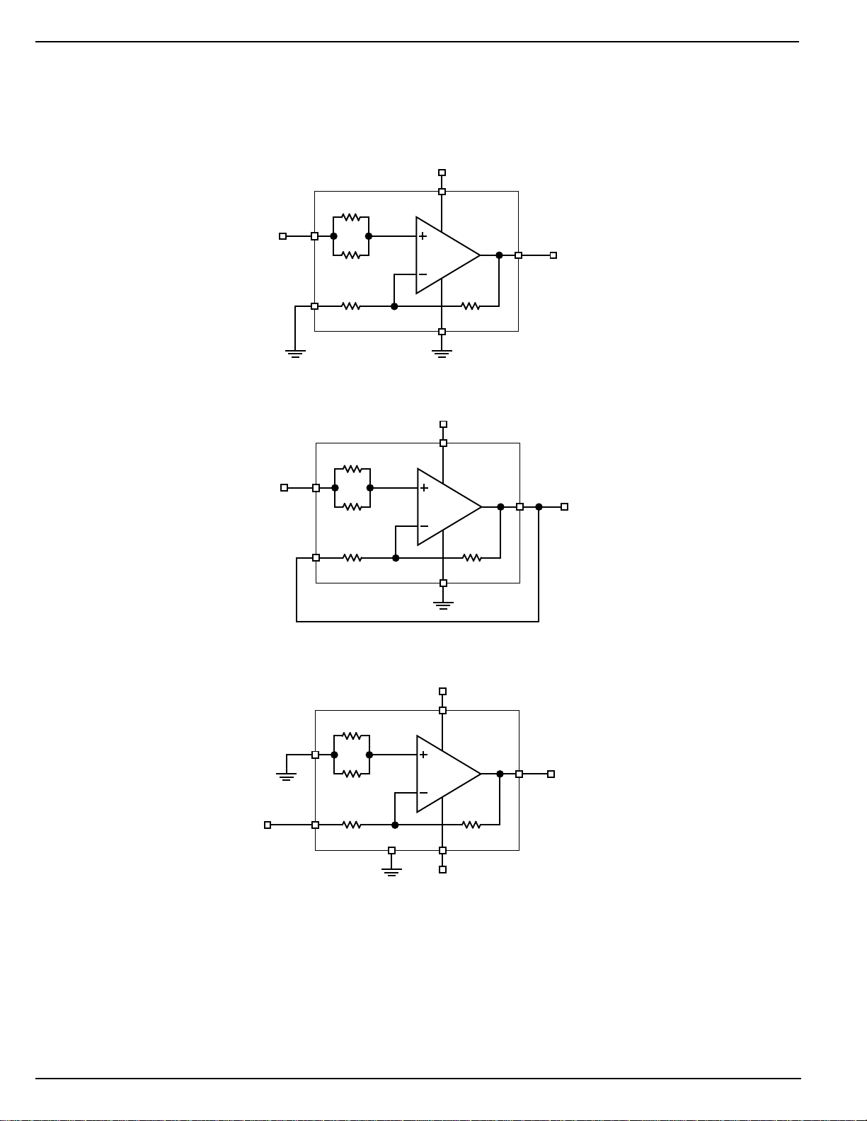
Figures 1 through 6 illustrate basic MIC6251 and MIC6252 GainBlock™ configurations.
+4V to +32V
5
V+
20k20k
2
5
MIC6251
MIC6251
OUT
1
OUT
1
V
= 2V
OUT
V
OUT
= V
IN
IN
20k
IN+
V
IN
3
20k
IN–
4
V–
Figure 1. MIC6251 AV = 2 Amplifier
+4V to +32V
V+
20k
IN+
V
IN
3
20k
IN–
4
V–
20k20k
2
Figure 2. MIC6251 Voltage Follower
+2V to +16V
5
V+
20k
MIC6251
IN+
3
20k
V
IN–
IN
4
3
GND
V–
20k20k
2
OUT
1
–2V to –16V
Figure 3. MIC6251 Inverting Unity-Gain Circuit
V
= –V
OUT
IN
MIC6251/6252 6 July 1998
Page 7
MIC6251/6252 Micrel
+4V to +32V
5
V+
MIC6252
IN+
V
IN
3
IN–
20k
20k
4
V–
20k
20k
2
OUT
1
V
OUT
V
IN
=
2
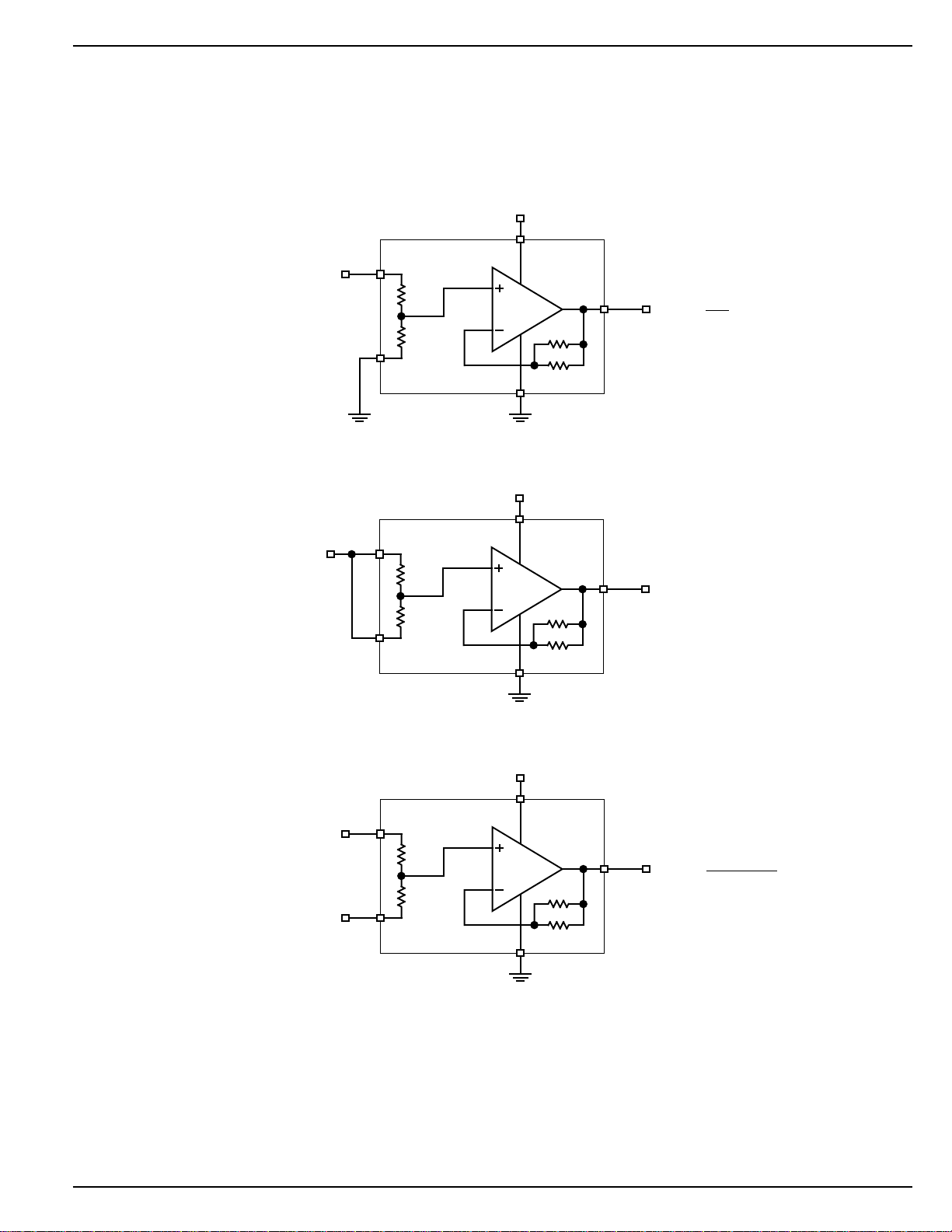
Figure 4. MIC6252 AV = 0.5 Amplifier
+4V to +32V
5
V+
2
MIC6252
20k
20k
OUT
1
V
= V
OUT
IN
V
IN+
IN
IN–
3
20k
20k
4
V–
Figure 5. MIC6252 Voltage Follower
+4V to +32V
5
V+
IN+
V
IN1
3
20k
IN–
V
IN2
20k
4
2
V–
Figure 6. MIC6252 Voltage Averager
MIC6252
20k
20k
OUT
1
V
OUT
VV
+
IN1 IN2
=
2
July 1998 7 MIC6251/6252
Page 8
MIC6251/6252 Micrel
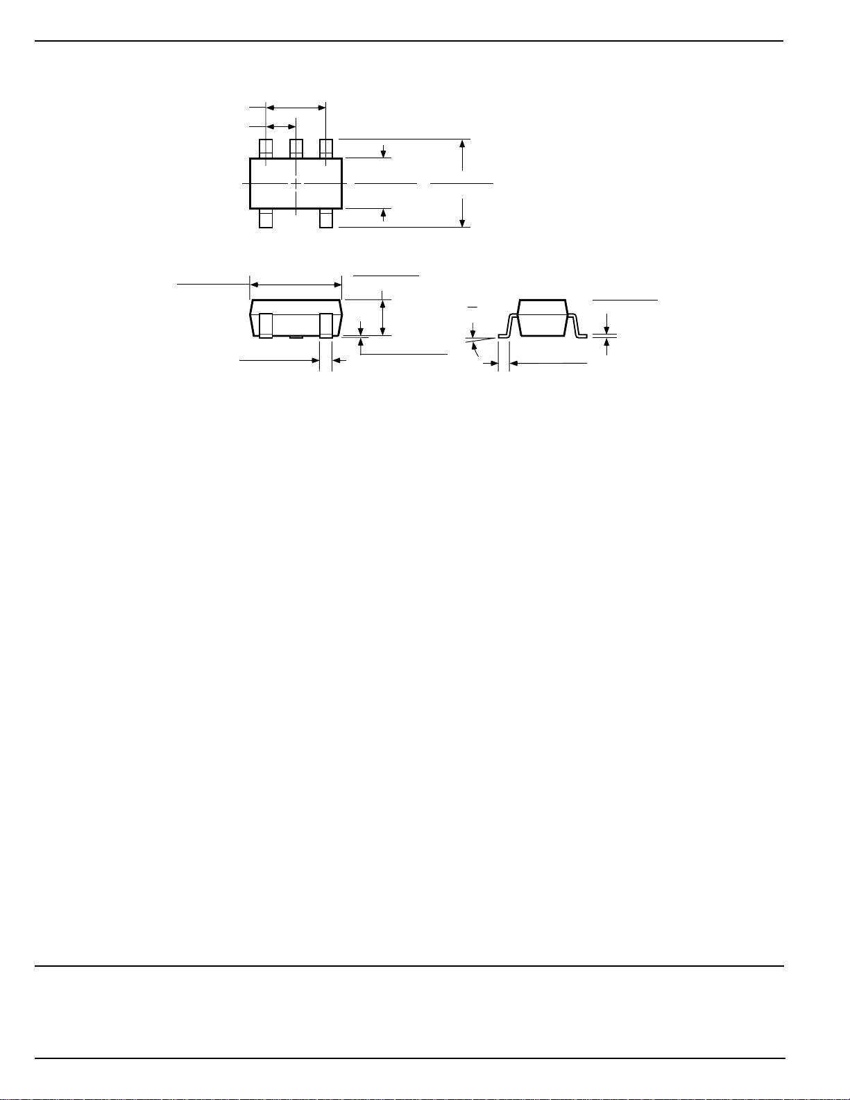
Package Information
1.90 (0.075) REF
0.95 (0.037) REF
3.02 (0.119)
2.80 (0.110)
0.50 (0.020)
0.35 (0.014)
1.75 (0.069)
1.50 (0.059)
1.30 (0.051)
0.90 (0.035)
0.15 (0.006)
0.00 (0.000)
SOT-23-5 (M5)
3.00 (0.118)
2.60 (0.102)
10°
0°
DIMENSIONS:
MM (INCH)
0.20 (0.008)
0.09 (0.004)
0.60 (0.024)
0.10 (0.004)
MICREL INC. 1849 FORTUNE DRIVE SAN JOSE, CA 95131 USA
TEL + 1 (408) 944-0800 FAX + 1 (408) 944-0970 WEB http://www.micrel.com
This information is believed to be accurate and reliable, however no responsibility is assumed by Micrel for its use nor for any infringement of patents or
other rights of third parties resulting from its use. No license is granted by implication or otherwise under any patent or patent right of Micrel Inc.
© 1998 Micrel Incorporated
MIC6251/6252 8 July 1998
 Loading...