

Page 1
MIC5891 Micrel
MIC5891
8-Bit Serial-Input Latched Source Driver
General Description
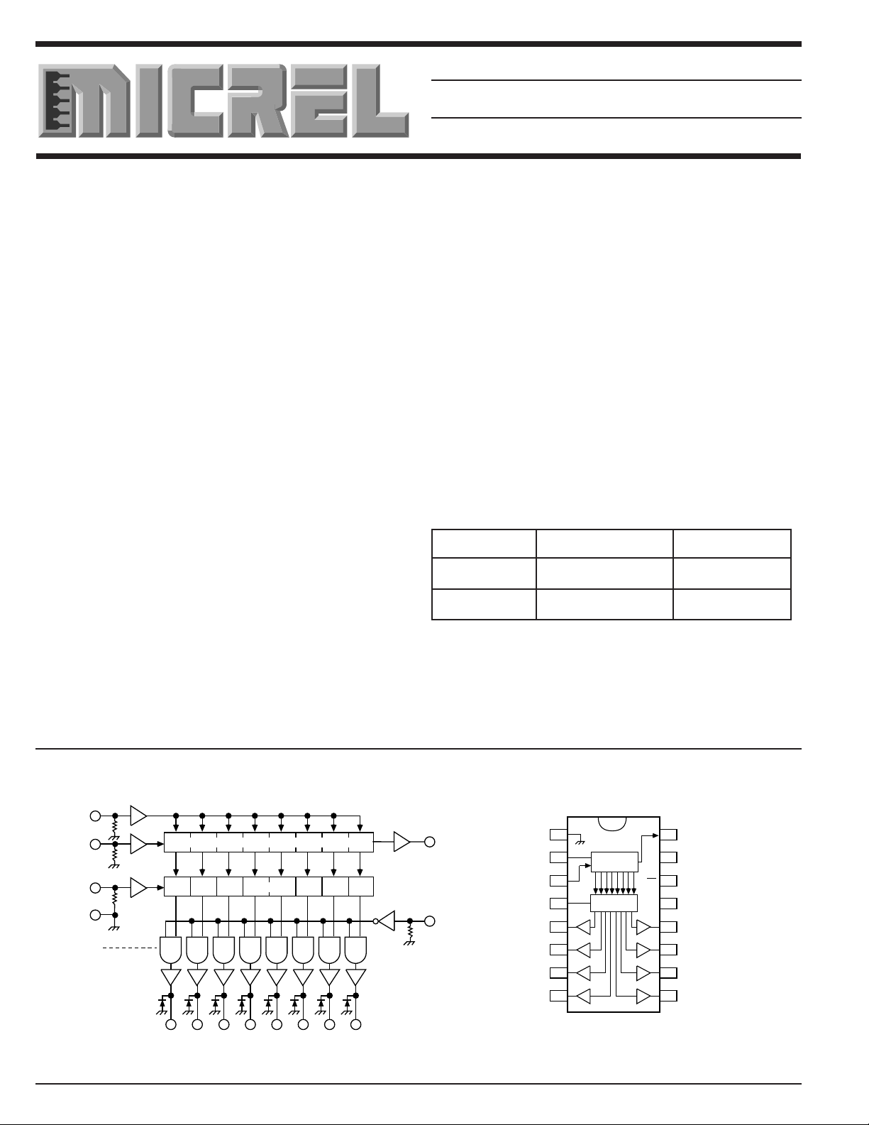
The MIC5891 latched driver is a high-voltage, high current
integrated circuit comprised of eight CMOS data latches,
CMOS control circuitry for the common STROBE and OUTPUT
ENABLE, and bipolar Darlington transistor drivers for each
latch.
Bipolar/MOS construction provides extremely low power
latches with maximum interface flexibility.
The MIC5891 will typically operate at 5MHz with a 5V logic
supply.
The CMOS inputs are compatible with standard CMOS,
PMOS, and NMOS logic levels. TTL circuits may be used with
appropriate pull-up resistors to ensure a proper logic-high
input.
A CMOS serial data output allows additional drivers to be
cascaded when more than 8 bits are required.
The MIC5891 has open-emitter outputs with suppression
diodes for protection against inductive load transients. The
output transistors are capable of sourcing 500mA and will
sustain at least 35V in the on-state.
Simultaneous operation of all drivers at maximum rated
current requires a reduction in duty cycle due to package
power limitations. Outputs may be paralleled for higher load
current capability.
The MIC5891 is available in a 16-pin plastic DIP package (N)
and 16-pin wide SOIC package (WM).
Features
• High-voltage, high-current outputs
• Output transient protection diodes
• CMOS-, PMOS-, NMOS-, and TTL-compatible inputs
• 5MHz typical data input rate
• Low-power CMOS latches
Applications
• Alphanumeric and bar graph displays
• LED and incandescent displays
• Relay and solenoid drivers
• Other high-power loads
Ordering Information
Part Number Temperature Range Package
MIC5891BN –40°C to +85°C 16-Pin Plastic DIP
MIC5891BWM –40°C to +85°C 16-pin Wide SOIC
Functional Diagram Pin Configurations
CLOCK
SERIAL
DATA IN
STROBE
GROUND
MOS
BIPOLAR
8-BIT SERIAL PARALLEL SHIFT REGISTER
LATCHES
OUT1OUT2OUT3OUT4OUT5OUT6OUT7OUT
SERIAL
DATA OUT
OUTPUT
ENABLE
8
GROUND
CLOCK
SERIAL
DATA IN
STROBE 4
7-54 December 1997
OUT
1
OUT
2
OUT37
OUT
4
1
2
3
5
6
8
SHIFT
REGISTER
LATCHES
16
15
V
DD
14
OE
V
BB
12
11
10
9
SERIAL
DATA OUT
LOGIC SUPPLY
OUTPUT
ENABLE
LOAD SUPPLY13
OUT
8
OUT
7
OUT
6
OUT
5
Page 2
MIC5891 Micrel
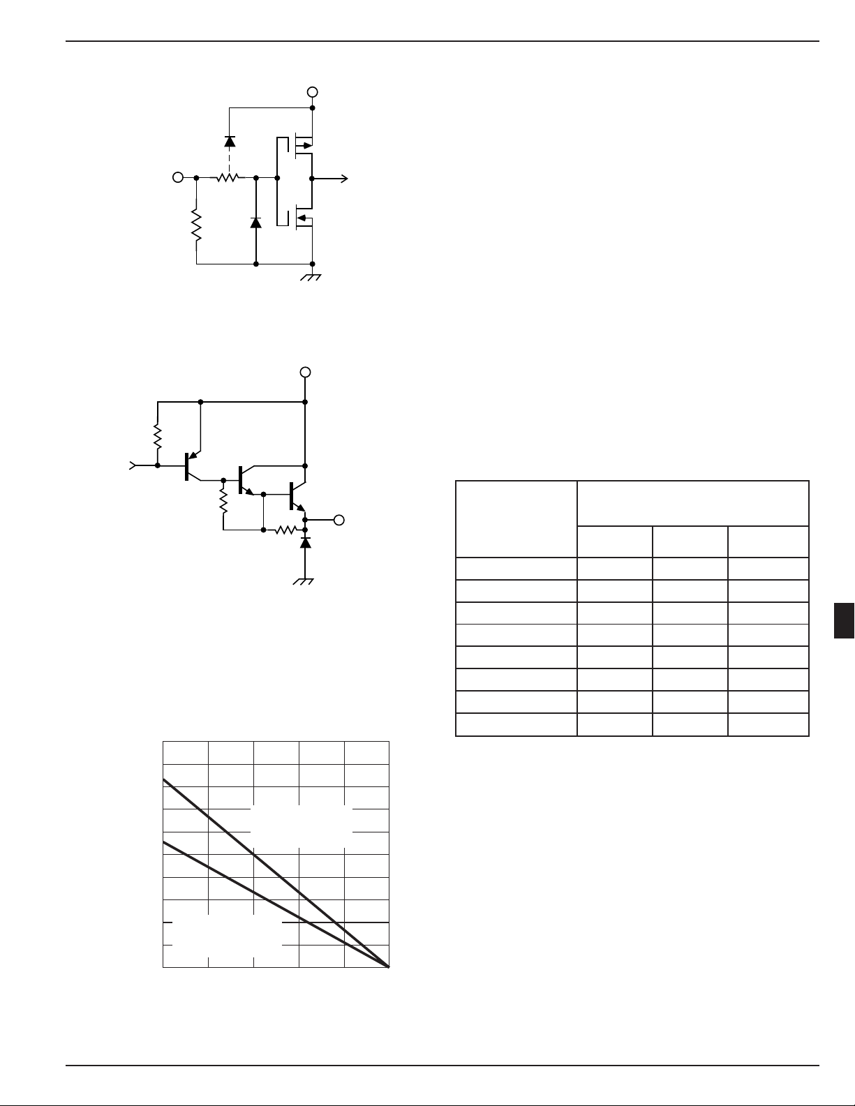
Typical Circuits
IN
Typical Input Circuit
V
DD
Output Voltage (V
) .............................................. 50V
OUT
Logic Supply Voltage Range (VDD)............... 4.5V to 15V
Load Supply Voltage Range (VBB)................ 5.0V to 50V
Input Voltage Range (VIN)................. –0.3V to VDD+0.3V
Continuous Collector Current (IC) ........................ 500mA
Package Power Dissipation .............................
see graph
Operating Temperature Range (TA)......–55°C to +125°C
Storage Temperature Range (TS).........–65°C to +150°C
Note 1: TA = 25°C
Note 2: Derate at the rate of 20mW/°C above TA = 25°C.
Note 3: Micrel CMOS devices have input-static protection but are
V
BB
susceptible to damage when exposed to extremely high static
electrical charges.
Allowable Duty Cycles
Absolute Maximum Ratings (Notes 1, 2, 3)
Typical Output Circuit
Allowable Package Power
Dissipation vs. Temp.
2.5
2
PDIP
= 60°C/W
1.5
1
θ
JA
V
OUT
Number of
Outputs ON at
I
= –200 mA
OUT
Max. Allowable Duty Cycles
at TA of:
50°C60°C70°C
8 53% 47% 41%
7 60% 54% 48%
6 70% 64% 56%
5 83% 75% 67%
4 100% 94% 84%
3 100% 100% 100%
2 100% 100% 100%
1 100% 100% 100%
7
0.5
CerDIP
= 90°C/W
θ
JA
0
25 50 75 100 125 150
PACKAGE POWER DISSIPATION (W)
AMBIENT TEMPERATURE (°C)
December 1997 7-55
Page 3
MIC5891 Micrel
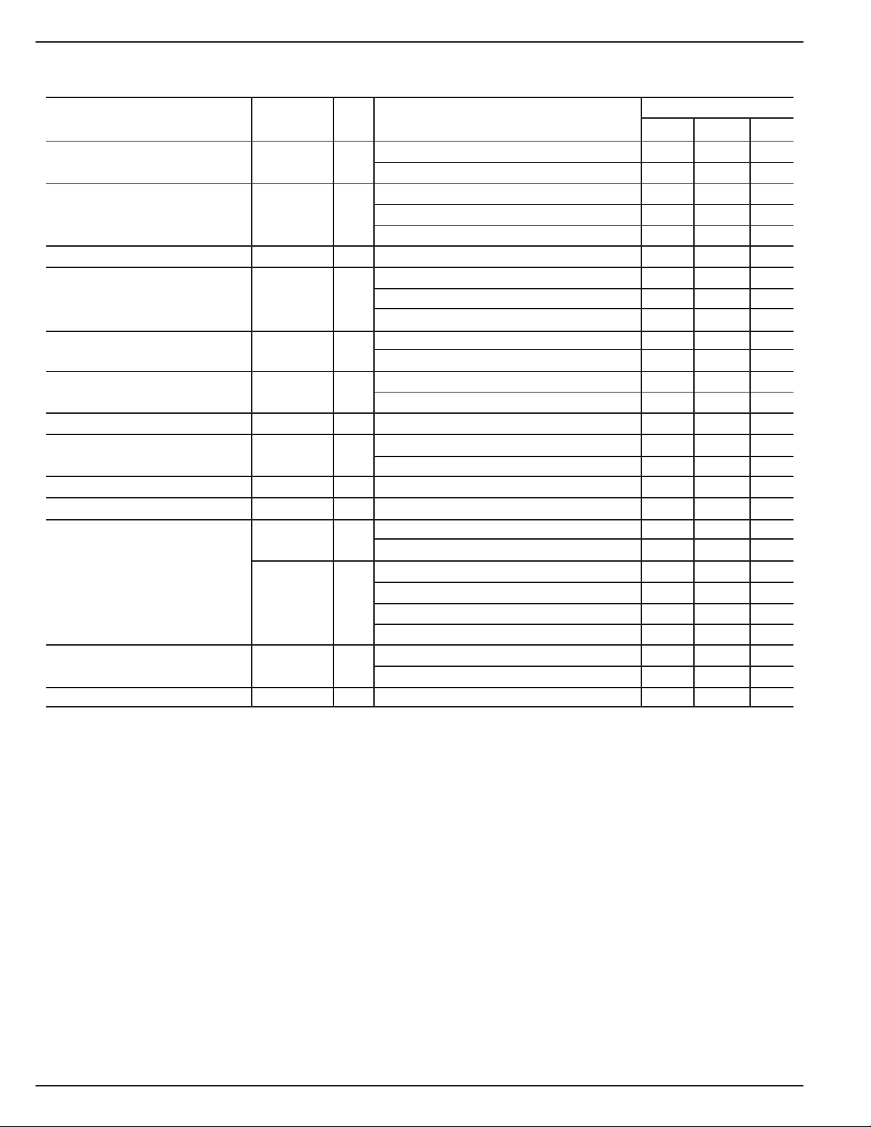
Electrical Characteristics
VBB = 50V, VDD = 5V to 12V; TA = +25°C; unless noted.
Limits
Characteristic Symbol V
Output Leakage Current I
Output Saturation Voltage V
Output Sustaining Voltage V
Input Voltage V
Input Current I
Input Impedance Z
Maximum Clock Frequency f
Serial Data Output Resistance R
Turn-On Delay t
Turnoff Delay t
Supply Current I
Diode Leakage Current I
Diode Forward Voltage V
Note 4: Positive (negative) current is defined as going into (coming out of) the specified device pin.
Note 5: Operation of these devices with standard TTL may require the use of appropriate pull-up resistors.
CEX
CE(SAT)
CE(SUS)
IN(1)
V
IN(0)
IN(1)
IN
c
OUT
PLH
PHL
BB
I
DD
H
F
50V TA = +25°C –50 µA
50V I
50V I
50V VDD = 5.0V 3.5 VDD+0.3 V
50V V
50V VDD = VIN = 5.0V 50 µA
50V VDD = 5.0V 100 kΩ
50V 3.3 MHz
50V VDD = 5.0V 20 kΩ
50V Output Enable to Output, I
50V Output Enable to Output, I
50V all outputs on, all outputs open 10 mA
50V VDD = 5V, all outputs off, inputs = 0V 100 µA
Max TA = +25°C50µA
Open IF = 350mA 2.0 V
Test Conditions Min. Max. Units
BB
TA = +85°C –100 µA
= –100mA, TA = +85°C 1.8 V
OUT
I
= –225mA, TA = +85°C 1.9 V
OUT
I
= –350mA, TA = +85°C 2.0 V
OUT
= –350mA, L = 2mH 35 V
OUT
V
= 12V 10.5 VDD+0.3 V
DD
= 5V to 12V VSS–0.3 0.8 V
DD
VDD = 12V 240 µA
V
= 12V 50 kΩ
DD
V
= 12V 6.0 kΩ
DD
= –350mA 2.0 µs
OUT
= –350mA 10 µs
OUT
all outputs off 200 µA
V
= 12V, all outputs off, inputs = 0V 200 µA
DD
VDD = 5V, one output on, all inputs = 0V 1.0 mA
VDD = 12V, one output on, all inputs = 0V 3.0 mA
T
= +85°C 100 µA
A
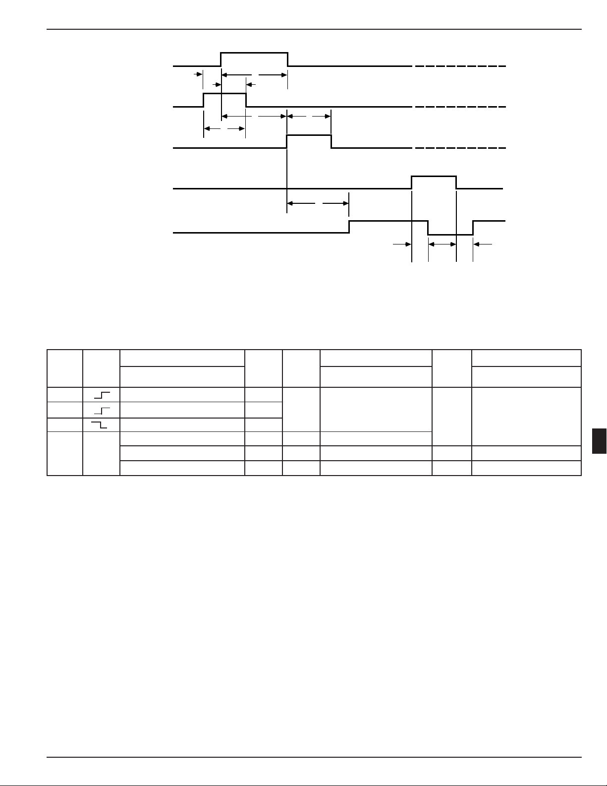
Timing Conditions
(VDD = 5.0V, Logic Levels are VDD and Ground)
A. Minimum data active time before clock pulse (data set-up time) ........................................................................75ns
B. Minimum data active time after clock pulse (data hold time) ..............................................................................75ns
C. Minimum data pulse width.................................................................................................................................150ns
D. Minimum clock pulse width ...............................................................................................................................150ns
E. Minimum time between clock activation and strobe ..........................................................................................300ns
F. Minimum strobe pulse width..............................................................................................................................100ns
G. Typical time between strobe activation and output transition.............................................................................1.0µs
H. Turnoff delay ................................................................................................................see Electrical Characteristics
I. Turn-on delay ............................................................................................................... see Electrical Characteristics
7-56 December 1997
Page 4
MIC5891 Micrel
CLOCK
A
D
B
DATA IN
FE
C
STROBE
OUTPUT
ENABLE
G
OUT
N
H I
Timing Conditions
T ruth Tab le
Serial Shift Register Contents Serial Latch Contents Output Content
Data Clock Data Strobe Output
Input Input I1I2I3…I
HHR
LLR
XR
R
1
2
R
1
2
R
R
1
2
3
N-1IN
…R
N-2RN-1
…R
N-2RN-1
…R
N-1RN
XXX …XX X L R1R2R3…R
P1P2P3…P
N-1PN
Output Input I1I2I3…I
R
N-1
R
N-1
R
N
P
N
HP1P2P3…P
N-1In
N-1RN
N-1PN
Enable I1I2I3…I
LP1P2P
…P
3
XXX…XX H LLL…LL
L = Low Logic Level
H = High Logic Level
X = Irrelevant
P = Present State
R = Previous State
Applications Information
Serial data present at the input is transferred into the shift
register on the rising edge of the CLOCK input pulse. Additional
CLOCK pulses shift data information towards the SERIAL
DATA OUTPUT. The serial data must appear at the input prior
to the rising edge of the CLOCK input waveform.
The 8 bits present in the shift register are transferred to the
respective latches when the STROBE is high (serial-toparallel conversion). The latches will continue to accept new
data as long as the STROBE is held high. Most applications
where the latching feature is not used (STROBE tied high)
require the OUTPUT ENABLE input to be high during serial
data entry.
Outputs are active (controlled by the latch state) when the
OUTPUT ENABLE is low. All Outputs are low (disabled) when
the OUTPUT ENABLE is high. OUTPUT ENABLE does not
affect the data in the shift register or latch.
N-1In
7
N-1PN
December 1997 7-57
 Loading...