

Page 1
MIC5821/5822
8-Bit Serial-Input Latched Drivers
MicrelMIC5821/5822
General Description
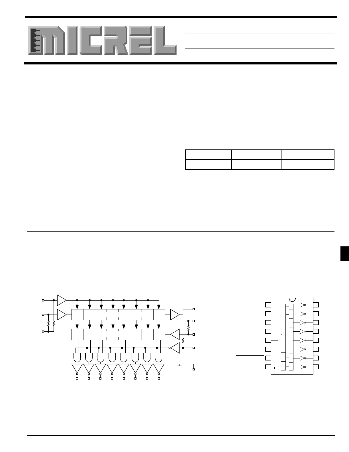
BiCMOS technology gives the MIC5821/5822 family flexibility beyond the reach of standard logic buffers and power
driver arrays. These devices each have an eight-bit CMOS
shift register, CMOS control circuitry, eight CMOS data
latches, and eight bipolar current-sink Darlington output
drivers. The 500mA outputs are suitable for use with incandescent bulbs and other moderate to high current loads. The
drivers can be operated with a split supply where the negative
supply is down to –20V. Except for maximum driver output
voltage ratings, the MIC5821 and MIC5822 are identical.
These devices have greatly improved data-input rates. With
a 5V logic supply they will typically operate faster than 5
MHz. With a 12V supply significantly higher speeds are
obtained. The CMOS inputs are compatible with standard
CMOS, PMOS, and NMOS logic levels. TTL and DTL circuits
may require the use of appropriate pull-up resistors. By using
the serial data output, the drivers can be cascaded for
interface applications requiring additional drive lines.
Features
• 3.3 MHz Minimum Data-Input Rate
• CMOS, PMOS, NMOS, TTL Compatible
• Internal Pull-Down or Pull-Up Resistors
• Low-Power CMOS Logic and Latches
• High-Voltage Current-Sink Outputs
• Single or Split Supply Operation
Ordering Information
Part Number Temperature Range Package
MIC5821BN –40°C to +85°C 16-Pin Plastic DIP
MIC5822BN –40°C to +85°C 16-Pin Plastic DIP
Functional Diagram
CLK
1
SERIAL
2
DATA IN
V
SS
3
OUT
OUT
1
8-BIT SERIAL-PARALLEL SHIFT REGISTER
LATCHES
OUT
OUT
OUT
3
2
5
4
OUT
7
Pin Configuration
CLOCK
SERIAL
5
DATA OUT
V
DD
4
STROBE
6
OUTPUT ENABLE
7
MOS
Bipolar
Sub
10111213141516
9
OUT
OUT
6
8
7
(ACTIVE LOW)
GND
8
V
EE
SERIAL DATA IN
SERIAL DATA OUT
STROBE
OUTPUT ENABLE
1
2
V
3
SS
V
DD
4
5
6
7
8
V
EE
SUB
LATCHES
SHIFT REGISTER
(Plastic DIP)
16
OUT
1
15
OUT
2
14
OUT
3
13
OUT
4
12
OUT
5
11
OUT
6
10
OUT
7
9
OUT
8
October 1998 7-37
Page 2
MicrelMIC5821/5822
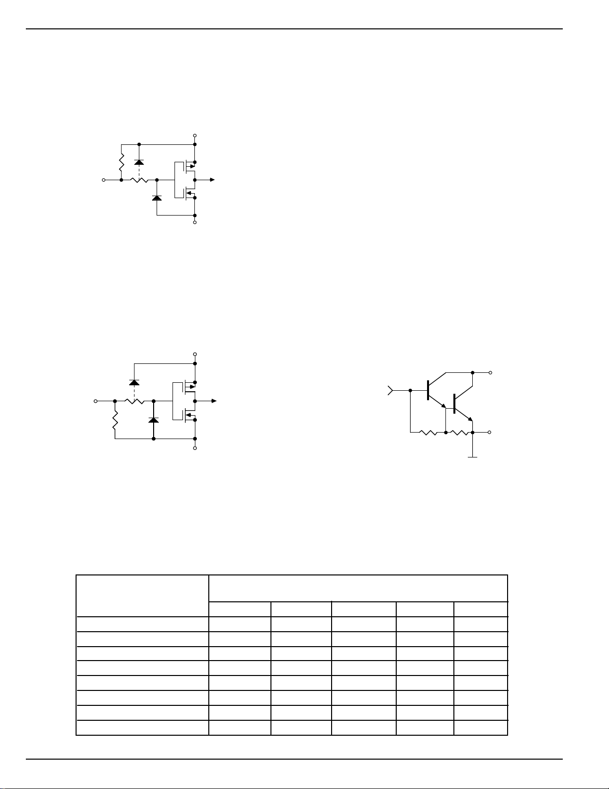
Typical Input Circuits
STROBE
OUTPUT
ENABLE
Absolute Maximum Ratings (Note 1)
at 25°C Free-Air Temperature and VSS = 0V
Output Voltage, V
Output Voltage, V
V
DD
Logic Supply Voltage, V
Input Voltage Range, V
VDD – V
EE
CE
CE SUS
Emitter Supply Voltage, V
Continuous Output Current, I
Package Power Dissipation, P
Operating Temperature Range, T
Storage Temperature Range, T
V
SS
Note 1: Derate at the rate of 16.7mW/°C above TA = 25°C.
Note 2: CMOS devices have input static protection but are susceptible to
damage when exposed to extremely high static electrical
charges.
Note 3: For inductive load applications.
(MIC5821) 50V
(MIC5822) 80V
(MIC5821)(Note 3) 35V
(MIC5822)(Note 3) 50V
DD
IN
EE
OUT
D(Note 1)
–0.3V to VDD + 0.3V
A
S
–55°C to +85°C
–65°C to +150°C
15V
25V
–20V
500mA
1.67W
V
DD
CLOCK
SERIAL
DATA IN
V
SS
Maximum Allowable Duty Cycle (Plastic DIP)
Number of Outputs ON
(I
= 200mA Maximum Allowable Duty Cycle at Ambient Temperature of
OUT
VDD = 12V) 25°C40°C50°C60°C70°C
8 73% 62% 55% 47% 40%
7 83% 71% 62% 54% 46%
6 97% 82% 72% 63% 53%
5 100% 98% 87% 75% 63%
4 100% 100% 100% 93% 79%
3 100% 100% 100% 100% 100%
2 100% 100% 100% 100% 100%
1 100% 100% 100% 100% 100%
Typical Output Driver
OUT
N
3K7.2K
SUB
V
EE
7-38 October 1998
Page 3
MicrelMIC5821/5822
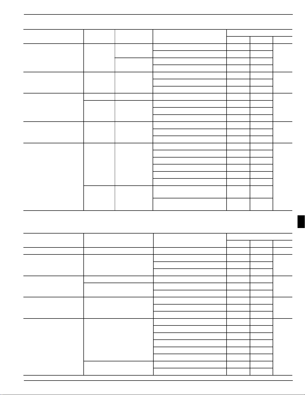
Electrical Characteristics at T
= 25°C VDD = 5V, V
A
= VSS = 0V (unless otherwise specified)
EE
Applicable Limits
Characteristic Symbol Devices Test Conditions Min. Max. Unit
Output Leakage Current I
Collector-Emitter V
CEX
CE(SAT)
Saturation Voltage I
Input Voltage V
V
IN(0)
IN(1)
MIC5821 V
MIC5822 V
Both I
= 50V 50 µA
OUT
V
= 50V, TA = +70°C 100
OUT
= 80V 50
OUT
V
= 80V, TA = +70°C 100
OUT
= 100mA 1.1 V
OUT
= 200mA 1.3
OUT
I
= 350mA, VDD = 7.0V 1.6
OUT
Both 0.8 V
Both VDD = 12V 10.5
VDD = 10V 8.5
VDD = 5.0V 3.5
Input Resistance R
IN
Both VDD = 12V 50 kΩ
VDD = 10V 50
VDD = 5.0V 50
Supply Current I
DD(ON)
Both One Driver ON, VDD = 12V 4.5 mA
One Driver ON, VDD = 10V 3.9
One Driver ON, VDD = 5.0V 2.4
All Drivers ON, VDD = 12V 16
All Drivers ON, VDD = 10V 14
All Drivers ON, VDD = 5.0V 8
I
DD(OFF)
Both All Drivers OFF, VDD = 5.0V, 1.6
All Inputs = 0V
All Drivers OFF, V
= 12V, 2.9
DD
All Inputs= 0V
Electrical Characteristics T
= –55°C, VDD = 5V, VSS = VEE = 0V (unless otherwise noted)
A
Limits
Characteristic Symbol Test Conditions Min. Max. Unit
Output Leakage Current I
Collector-Emitter V
CEX
CE(SAT)
Saturation Voltage I
Input Voltage V
V
IN0)
IN(1)
V
= 80V 50 µA
OUT
I
= 100mA 1.3 V
OUT
= 200mA 1.5
OUT
I
= 350mA, VDD = 7.0V 1.8
OUT
0.8 V
VDD = 12V 10.5
VDD = 5.0V 3.5
Input Resistance RIN VDD = 12V 35 kΩ
VDD = 10V 35
VDD = 5.0V 35
Supply Current I
DD(ON)
One Driver ON, VDD = 12V 5.5 mA
One Driver ON, VDD = 10V 4.5
One Driver ON, VDD = 5.0V 3.0
All Drivers ON, VDD = 12V 16
All Drivers ON, VDD = 10V 14
All Drivers ON, VDD = 5.0V 10
I
DD(OFF)
All Drivers OFF, VDD = 12V 3.5
All Drivers OFF, VDD = 5.0V 2.0
7
October 1998 7-39
Page 4
MicrelMIC5821/5822
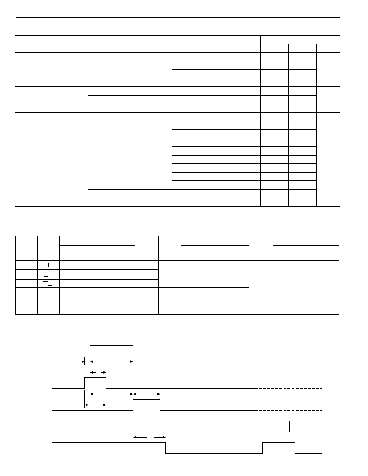
Electrical Characteristics T
= +125°C, VDD = 5V, VSS = VEE = 0V (unless otherwise noted)
A
Limits
Characteristic Symbol Test Conditions Min. Max. Unit
Output Leakage Current I
Collector-Emitter V
CEX
CE(SAT)
Saturation Voltage I
Input Voltage V
V
IN(0)
IN(1)
V
= 80V 500 µA
OUT
I
= 100mA 1.3 V
OUT
= 200mA 1.5
OUT
I
= 350mA, VDD = 7.0V 1.8
OUT
0.8 V
VDD = 12V 10.5
VDD = 5.0V 3.5
Input Resistance R
IN
VDD = 12V 50 kΩ
VDD = 10V 50
VDD = 5.0V 50
Supply Current I
DD(ON)
One Driver ON, VDD = 12V 4.5 mA
One Driver ON, VDD = 10V 3.9
One Driver ON, VDD = 5.0V 2.4
All Drivers ON, VDD = 12V 16
All Drivers ON, VDD = 10V 14
All Drivers ON, VDD = 5.0V 8
I
DD(OFF)
All Drivers OFF, VDD = 12V 2.9
All Drivers OFF, VDD = 5.0V 1.6
MIC5821/5822 Family Truth Table
Serial Shift Register Contents Serial Latch Contents Output Contents
Data Clock Data Strobe Output
Input Input I
HHR
LLR
XR
1I2I3
1R2
1R2
1R2R3
XXX……X X L R1R2R3…… R
P1P2P3…… P
…… I
…… R
…… R
…… R
Output Input I1I
8
7
7
8
8
R
7
R
7
R
8
P
8
2I3
…… I8Enable I1I
HP1P2P3…… P
2I3
8
LP1P2P3…… P
8
…… I
X X X …… X H H H H …… H
L = Low Logic Level H = High Logic Level X = Irrelevant P = Present State R = Previous State
Timing Diagram
CLOCK
A
DATA IN
D
B
E
F
8
8
STROBE
OUTPUT
ENABLE
OUT
C
G
N
7-40 October 1998
Page 5
MicrelMIC5821/5822
Timing Conditions
(TA = +25°C, Logic Levels are VDD and VSS)
VDD = 5.0V
A. Minimum Data Active Time Before Clock Pulse (Data Set-Up Time) .......................................................................75 ns
B. Minimum Data Active Time After Clock Pulse (Data Hold Time).............................................................................75 ns
C. Minimum Data Pulse Width ....................................................................................................................................150 ns
D. Minimum Clock Pulse Width...................................................................................................................................150 ns
E. Minimum Time Between Clock Activation and Strobe ............................................................................................300 ns
F. Minimum Strobe Pulse Width..................................................................................................................................100 ns
G. Typical Time Between Strobe Activation and Output Transition .............................................................................500 ns
SERIAL DATA present at the input is transferred to the shift register on the logic “0” to logic “1” transition of the CLOCK input
pulse. On succeeding CLOCK pulses, the registers shift data information towards the SERIAL DATA OUTPUT. The SERIAL
DATA must appear at the input prior to the rising edge of the CLOCK input waveform.
Information present at any register is transferred to its respective latch when the STROBE is high (serial-to-parallel conversion).
The latches will continue to accept new data as long as the STROBE is held high. Applications where the latches are bypassed
(STROBE tied high) will require that the ENABLE input be high during serial entry.
When the ENABLE input is high, all of the output buffers are disabled (OFF) without affecting the information stored in the
latches or shift register. With the ENABLE input low, the outputs are controlled by the state of the latches.
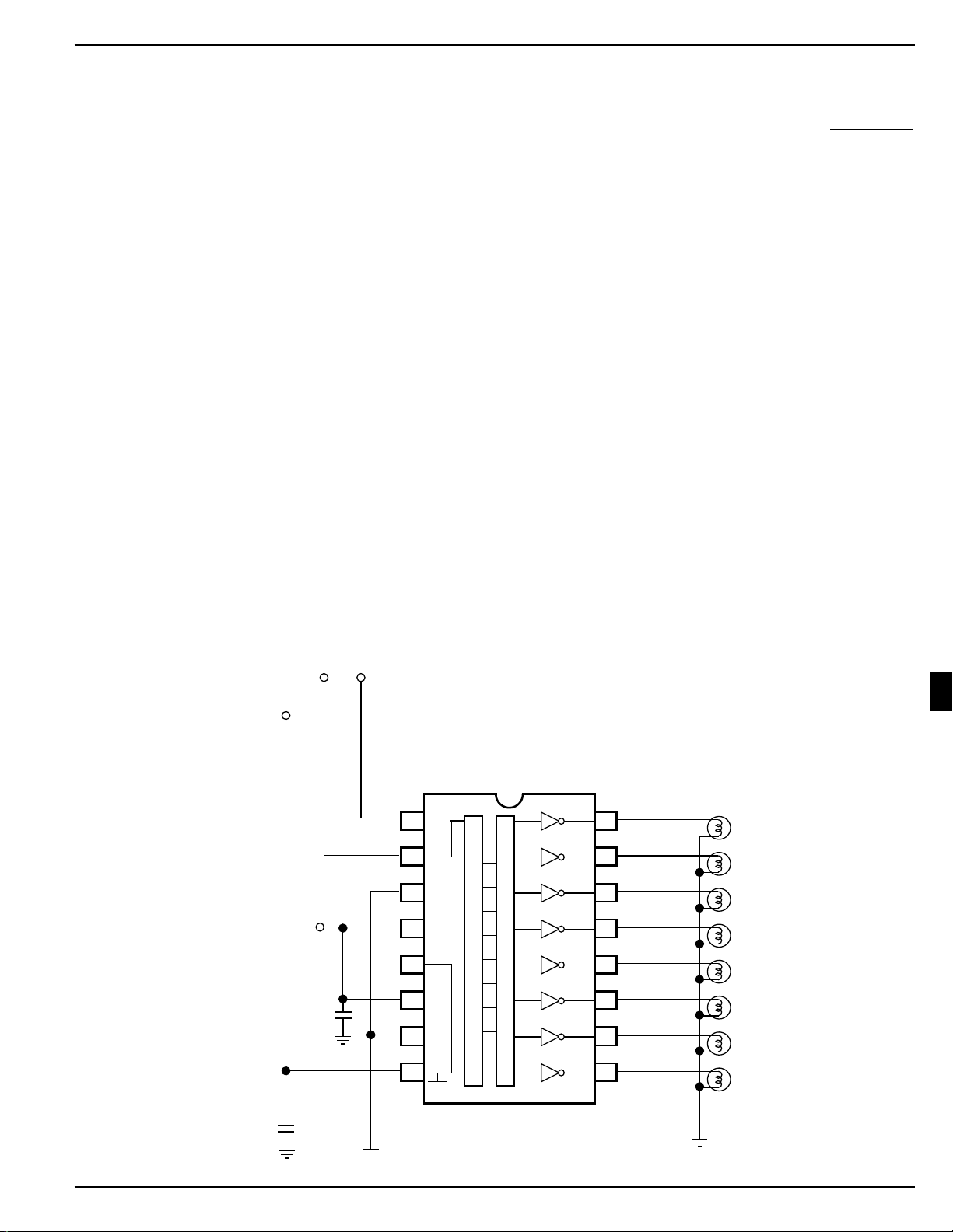
Typical Applications
MIC5822 Level Shifting Lamp Driver with Darlington Emitters Tied to a Negative Supply
SERIAL DATA CLOCK
-9V
+5V
7
1
2
3
4
16
15
14
13
5
+
0.1µ
6
7
8
SUB
100µ
SHIFT REGISTER
October 1998 7-41
LATCHES
12
11
10
9
 Loading...