

Page 1
MIC5207 Micrel
MIC5207
180mA Low-Noise LDO Regulator
General Description
The MIC5207 is an efficient linear voltage regulator with ultralow-noise output, very low dropout voltage (typically 17mV at
light loads and 165mV at 150mA), and very low ground
current (720µA at 100mA output). The MIC5207 offers better
than 3% initial accuracy.
Designed especially for hand-held, battery-powered devices,
the MIC5207 includes a CMOS or TTL compatible enable/
shutdown control input. When shutdown, power consumption drops nearly to zero.
Key MIC5207 features include a reference bypass pin to
improve its already low-noise performance, reversed-battery
protection, current limiting, and overtemperature shutdown.
The MIC5207 is available in fixed and adjustable output
voltage versions in a small SOT-23-5 package. Contact
Micrel for details.
For low-dropout regulators that are stable with ceramic
output capacitors, see the µCap MIC5245/6/7 family.
Ordering Information
Part Number* Marking Voltage Junction Temp. Range Package
MIC5207BM5 LEAA Adj –40°C to +125°C SOT-23-5
MIC5207-1.8BM5 LE18 1.8 0°C to +125°C SOT-23-5
MIC5207-2.5BM5 LE25 2.5 –40°C to +125°C SOT-23-5
MIC5207-3.0BM5 LE30 3.0 –40°C to +125°C SOT-23-5
MIC5207-3.3BM5 LE33 3.3 –40°C to +125°C SOT-23-5
MIC5207-3.6BM5 LE36 3.6 –40°C to +125°C SOT-23-5
MIC5207-3.8BM5 LE38 3.8 –40°C to +125°C SOT-23-5
MIC5207-4.0BM5 LE40 4.0 –40°C to +125°C SOT-23-5
MIC5207-5.0BM5 LE50 5.0 –40°C to +125°C SOT-23-5
MIC5207-3.3BZ — 3.3 –40°C to +125°C TO-92
* Other voltages available. Contact Micrel Marketing for information.
Features
• Ultra-low-noise output
• High output voltage accuracy
• Guaranteed 180mA output
• Low quiescent current
• Low dropout voltage
• Extremely tight load and line regulation
• Very low temperature coefficient
• Current and thermal limiting
• Reverse-battery protection
•“Zero” off-mode current
• Logic-controlled electronic enable
Applications
• Cellular telephones
• Laptop, notebook, and palmtop computers
• Battery-powered equipment
• PCMCIA VCC and V
• Consumer/personal electronics
• SMPS post-regulator/dc-to-dc modules
• High-efficiency linear power supplies
regulation/switching
PP
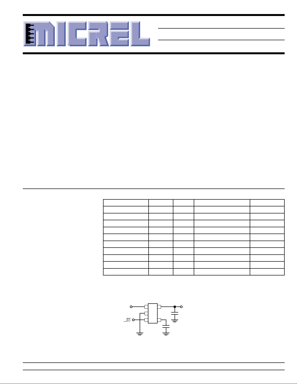
Typical Application
MIC5207-x.xBM5
V
IN
15
2
Enable
Shutdown
EN (pin 3) may be
connected directly
to IN (pin 1).
Enable
3
4
Battery-Powered Regulator Application
Micrel, Inc. • 1849 Fortune Drive • San Jose, CA 95131 • USA • tel + 1 (408) 944-0800 • fax + 1 (408) 944-0970 • http://www.micrel.com
January 2000 1 MIC5207
V
OUT
C
OUT
tantalum
C
BYP
(OPTIONAL)
= 2.2µF
Low-Noise Operation:
= 470pF, C
C
BYP
OUT
≥ 2.2µF
Page 2
MIC5207 Micrel
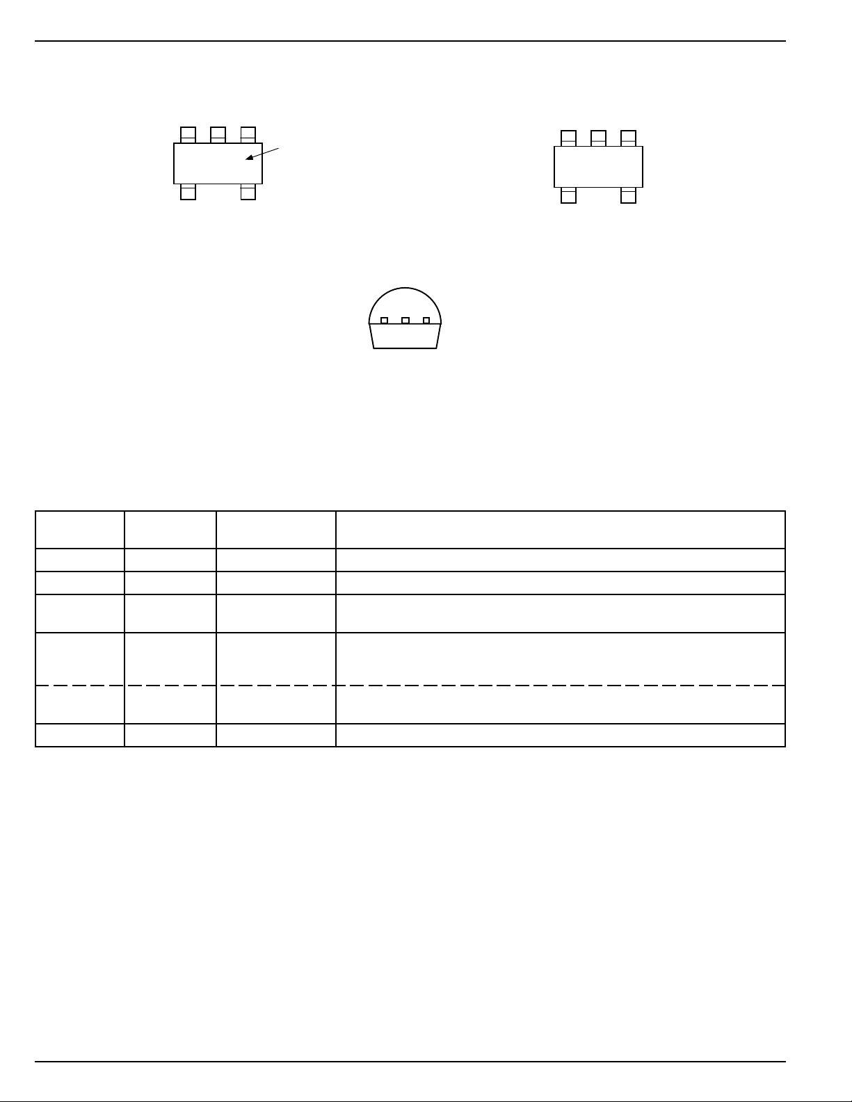
Pin Configuration
(Adjustable Voltage)
Pin Description
GND
2
IN
13
EN
LEAA
45
OUTADJ
MIC5207BM5
SOT-23-5
Part
Identification
123
IN OUTGND
(Bottom View)
MIC5207-x.xBZ
TO-92
(Fixed Voltages)
GND
2
IN
13
EN
LExx
45
OUTBYP
MIC5207-x.xBM5
SOT-23-5
(Fixed Voltages)
Pin No. Pin No. Pin Name Pin Function
SOT-23-5 TO-92
1 1 IN Supply Input
2 2 GND Ground
3 EN Enable/Shutdown (Input): CMOS compatible input. Logic high = enable,
logic low or open = shutdown.
4 (fix) BYP Reference Bypass: Connect external 470pF capacitor to GND to reduce
output noise. May be left open. For 1.8V or 2.5V operation, see “Applications
Information.”
4 (adj) ADJ Adjust (Input): Adjustable regulator feedback input. Connect to resistor
voltage divider.
5 3 OUT Regulator Output
Absolute Maximum Ratings (Note 1)
Supply Input Voltage (VIN) ............................ –20V to +20V
Enable Input Voltage (VEN) ........................... –20V to +20V
Power Dissipation (PD) ............... Internally Limited, Note 3
Lead Temperature (soldering, 5 sec.) ....................... 260°C
Junction Temperature (TJ)
all except 1.8V......................................–40°C to +125°C
Operating Ratings (Note 2)
Input Voltage (VIN) ....................................... +2.5V to +16V
Enable Input Voltage (VEN) .................................. 0V to V
Junction Temperature (TJ)
all except 1.8V......................................–40°C to +125°C
1.8V only ..................................................0°C to +125°C
Thermal Resistance (θJA).........................................Note 3
1.8V only ..................................................0°C to +125°C
Storage Temperature (TS) ....................... –65°C to +150°C
IN
MIC5207 2 January 2000
Page 3

MIC5207 Micrel
Electrical Characteristics
VIN = V
0°C ≤ TJ ≤ +125°C for 1.8V version; unless noted.
Symbol Parameter Conditions Min Typical Max Units
V
O
∆V
O
∆V
O/VO
∆V
O/VO
– V
V
IN
I
GND
I
GND
PSRR Ripple Rejection 75 dB
I
LIMIT
∆VO/∆P
e
no
ENABLE Input
V
IL
V
IH
I
IL
I
IH
+ 1V; IL = 100µA; CL = 1.0µF; VEN ≥ 2.0V; TJ = 25°C, bold values indicate –40°C ≤ TJ ≤ +125°C except
OUT
Output Voltage Accuracy variation from specified V
OUT
–33%
–44%
/∆T Output Voltage Note 4 40 ppm/°C
Temperature Coefficient
Line Regulation VIN = V
+ 1V to 16V 0.005 0.05 %/V
OUT
0.10 %/V
Load Regulation IL = 0.1mA to 150mA, Note 5 0.05 0.5 %
0.7 %
O
Dropout Voltage, Note 6 IL = 100µA1760mV
80 mV
IL = 50mA 115 175 mV
250 mV
IL = 100mA 140 280 mV
325 mV
= 150mA 165 300 mV
I
L
400 mV
Quiescent Current VEN ≤ 0.4V (shutdown) 0.01 1 µA
VEN ≤ 0.18V (shutdown) 5 µA
Ground Pin Current, Note 7 VEN ≥ 2.0V, IL = 100µA80130µA
170 µA
= 50mA 350 650 µA
I
L
900 µA
IL = 100mA 720 1100 µA
2000 µA
IL = 150mA 1800 2500 µA
3000 µA
Current Limit V
Thermal Regulation Note 8 0.05 %/W
D
Output Noise IL = 50mA, CL = 2.2µF, 260
= 0V 320 500 mA
OUT
nV Hz
470pF from BYP to GND
Enable Input Logic-Low Voltage regulator shutdown 0.4 V
0.18 V
Enable Input Logic-High Voltage regulator enabled 2.0 V
Enable Input Current VIL ≤ 0.4V 0.01 –1 µA
≤ 0.18V –2 µA
V
IL
VIH ≥ 2.0V 5 20 µA
VIH ≥ 2.0V 25 µA
Note 1. Exceeding the absolute maximum rating may damage the device.
Note 2. The device is not guaranteed to function outside its operating rating.
Note 3: The maximum allowable power dissipation at any TA (ambient temperature) is P
allowable power dissipation will cause excessive die temperature, and the regulator will go into thermal shutdown. The θJA of the SOT-23-5
(M5) is 235°C/W and the TO-92 (Z) is 180°C/W (0.4" leads) or 160°C/W (0.25" leads) soldered to a PC board. See “Thermal Considerations.”
Note 4: Output voltage temperature coefficient is defined as the worst case voltage change divided by the total temperature range.
Note 5: Regulation is measured at constant junction temperature using low duty cycle pulse testing. Parts are tested for load regulation in the load
range from 0.1mA to 180mA. Changes in output voltage due to heating effects are covered by the thermal regulation specification.
Note 6: Dropout voltage is the input to output differential at which the output voltage drops 2% below its nominal value measured at 1V differential.
Note 7: Ground pin current is the regulator quiescent current plus pass transistor base current. The total current drawn from the supply is the sum of
the load current plus the ground pin current.
Note 8: Thermal regulation is defined as the change in output voltage at a time “t” after a change in power dissipation is applied, excluding load or line
regulation effects. Specifications are for a 180mA load pulse at VIN = 16V for t = 10ms.
D(max)
= (T
– TA) ÷ θJA. Exceeding the maximum
J(max)
January 2000 3 MIC5207
Page 4
MIC5207 Micrel
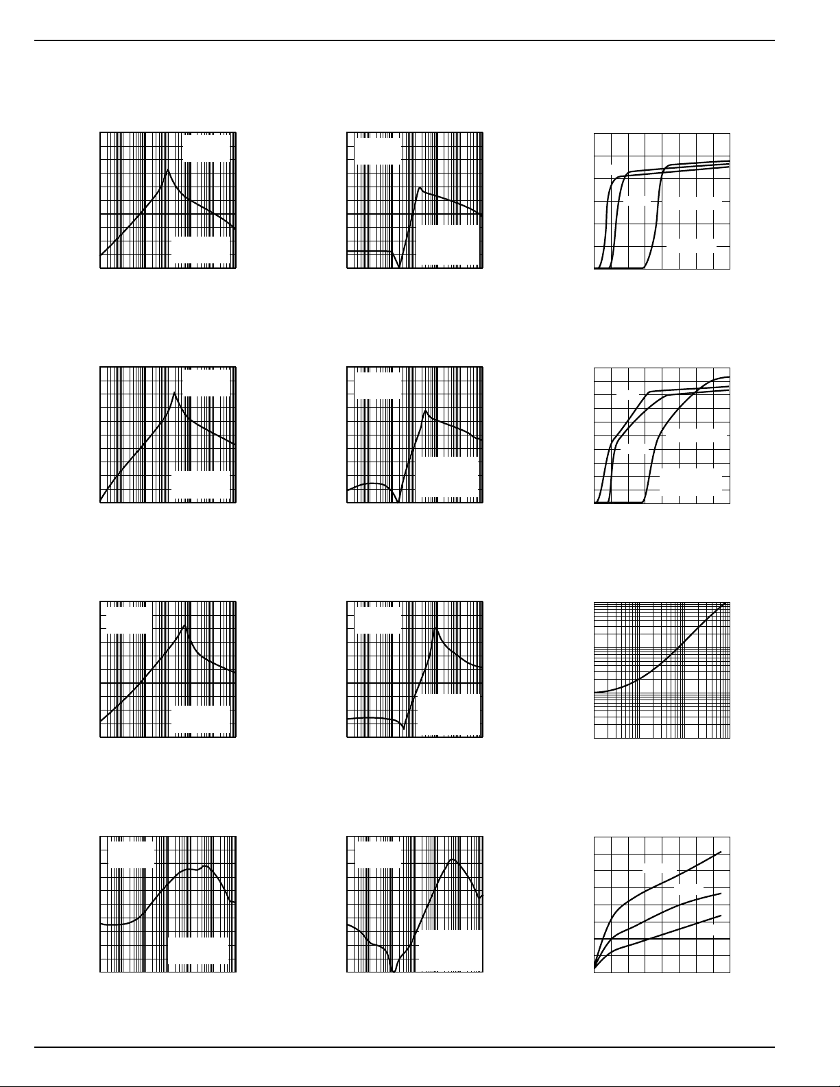
Typical Characteristics
Power Supply
Rejection Ratio
0
-20
VIN = 6V
V
= 5V
OUT
-40
-60
PSRR (dB)
-80
-100
1E+11E+21E+3 1E+41E+51E+61E+7
10
100
FREQUENCY (Hz)
I
= 100µA
OUT
C
= 1µF
OUT
1k
10k
100k
Power Supply
Rejection Ratio
0
-20
-40
-60
PSRR (dB)
-80
-100
1E+11E+21E+3 1E+41E+51E+61E+7
10
1k
100
FREQUENCY (Hz)
10k
VIN = 6V
V
I
OUT
C
OUT
100k
= 5V
OUT
= 1mA
= 1µF
1M
1M
10M
10M
Power Supply
Rejection Ratio
0
VIN = 6V
V
OUT
= 5V
-20
-40
-60
PSRR (dB)
-80
-100
1E+11E+21E+3 1E+41E+51E+61E+7
10
100
I
= 100µA
OUT
C
= 2.2µF
OUT
C
= 0.01µF
BYP
1k
10k
FREQUENCY (Hz)
100k
1M
Power Supply
Rejection Ratio
0
VIN = 6V
V
-20
-40
-60
PSRR (dB)
-80
-100
= 5V
OUT
I
= 1mA
OUT
C
= 2.2µF
OUT
C
= 0.01µF
BYP
1E+11E+21E+3 1E+41E+51E+61E+7
10
1k
100
10k
FREQUENCY (Hz)
100k
1M
10M
10M
Power Supply Ripple Rejection
vs. Voltage Drop
60
50
1mA
40
30
10mA
I
OUT
= 100mA
20
C
10
RIPPLE REJECTION (dB)
0
0 0.1 0.2 0.3 0.4
VOLTAGE DROP (V)
OUT
= 1µF
Power Supply Ripple Rejection
100
RIPPLE REJECTION (dB)
vs. Voltage Drop
90
80
1mA
70
60
50
40
10mA
30
20
10
0
0 0.1 0.2 0.3 0.4
VOLTAGE DROP (V)
I
C
OUT
C
BYP
= 100mA
OUT
= 2.2µF
= 0.01µF
Power Supply
Rejection Ratio
0
VIN = 6V
V
OUT
= 5V
-20
-40
-60
PSRR (dB)
-80
-100
1E+11E+21E+3 1E+41E+51E+61E+7
10
100
FREQUENCY (Hz)
I
= 10mA
OUT
C
= 1µF
OUT
1k
10k
100k
1M
Power Supply
Rejection Ratio
0
VIN = 6V
V
-20
-40
-60
PSRR (dB)
-80
-100
= 5V
OUT
I
= 100mA
OUT
C
= 1µF
OUT
1E+11E+21E+31E+41E+51E+61E+7
10
1k
100
10k
FREQUENCY (Hz)
100k
1M
10M
10M
Power Supply
Rejection Ratio
0
VIN = 6V
V
OUT
= 5V
-20
-40
-60
PSRR (dB)
-80
-100
1E+11E+21E+3 1E+41E+51E+61E+7
10
100
FREQUENCY (Hz)
I
= 10mA
OUT
C
= 2.2µF
OUT
C
= 0.01µF
BYP
1k
10k
100k
1M
Power Supply
Rejection Ratio
0
VIN = 6V
V
-20
-40
-60
PSRR (dB)
-80
-100
= 5V
OUT
I
= 100mA
OUT
C
= 2.2µF
OUT
C
= 0.01µF
BYP
1E+11E+21E+31E+41E+51E+61E+7
10
1k
100
10k
FREQUENCY (Hz)
100k
1M
10M
10M
Turn-On Time
vs. Bypass Capacitance
10000
1000
TIME (µs)
100
10
10 100 1000 10000
CAPACITANCE (pF)
Dropout Voltage
vs. Output Current
320
280
240
200
160
120
80
40
DROPOUT VOLTAGE (mV)
0
0 40 80 120 160
+125°C
+25°C
OUTPUT CURRENT (mA)
–40°C
MIC5207 4 January 2000
Page 5
MIC5207 Micrel
0.0001
0.001
0.01
0.1
1
10
1E+11E+21E+31E+41E+51E+61E+7
NOISE (µV/√Hz)
FREQUENCY (Hz)
√
√
0.0001
0.001
0.01
0.1
1
10
1E+11E+21E+31E+41E+51E+61E+7
NOISE (µV/√Hz)
FREQUENCY (Hz)
√
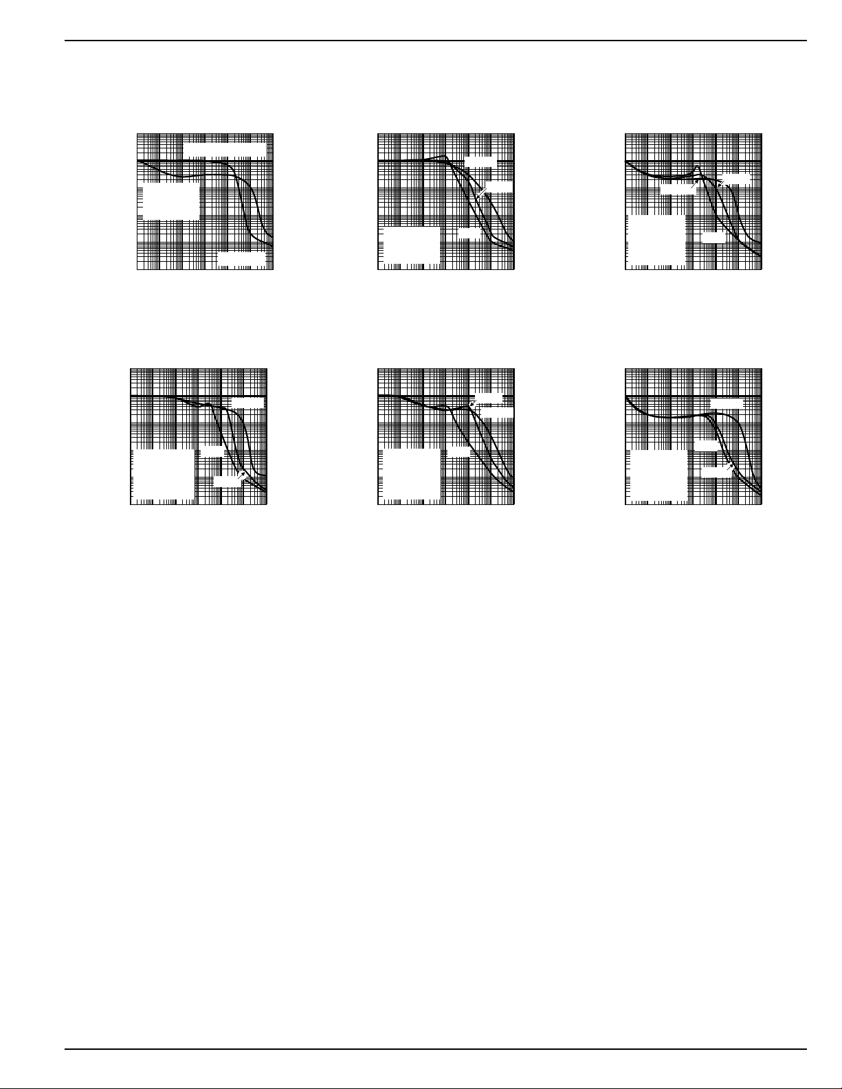
Typical Characteristics
Noise Performance
10
10mA, C
1
0.1
1mA
C
= 1µF
OUT
C
BYP
= 10nF
NOISE (µV/√Hz)
0.01
0.001
V
0.0001
1E+11E+21E+3 1E+41E+51E+61E+7
10
10
1k
100
10k 100k 1M 10M
FREQUENCY (Hz)
Noise Performance
1
Hz)
0.1
0.01
V
= 5V
NOISE (µV/
0.0001
OUT
C
= 10µF
OUT
0.001
electrolytic
C
= 100pF
BYP
1E+11E+21E+31E+41E+51E+61E+7
10
100
FREQUENCY (Hz)
1mA
10mA
1k
10k 100k1M10M
OUT
OUT
= 1µF
= 5V
100mA
Noise Performance
V
= 5V
OUT
C
= 10µF
OUT
electrolytic
100
1k
10
Noise Performance
V
= 5V
OUT
C
= 10µF
OUT
electrolytic
C
= 1nF
BYP
100
1k
10
100mA
10mA
1mA
10k 100k1M10M
10mA
100mA
1mA
10k 100k1M10M
Noise Performance
10
1
Hz)
0.1
0.01
NOISE (µV/
0.001
0.0001
1E+11E+21E+31E+41E+51E+61E+7
10
10
1
Hz)
0.1
0.01
NOISE (µV/
0.001
0.0001
1E+11E+21E+31E+41E+51E+61E+7
10
100mA
V
= 5V
OUT
C
= 22µF
OUT
tantalum
C
= 10nF
BYP
1k
100
10k 100k1M10M
FREQUENCY (Hz)
Noise Performance
V
= 5V
OUT
C
= 10µF
OUT
electrolytic
C
= 10nF
BYP
FREQUENCY (Hz)
1mA
1k100
10k
1mA
100mA
10mA
100k
10mA
1M
10M
January 2000 5 MIC5207
Page 6
MIC5207 Micrel
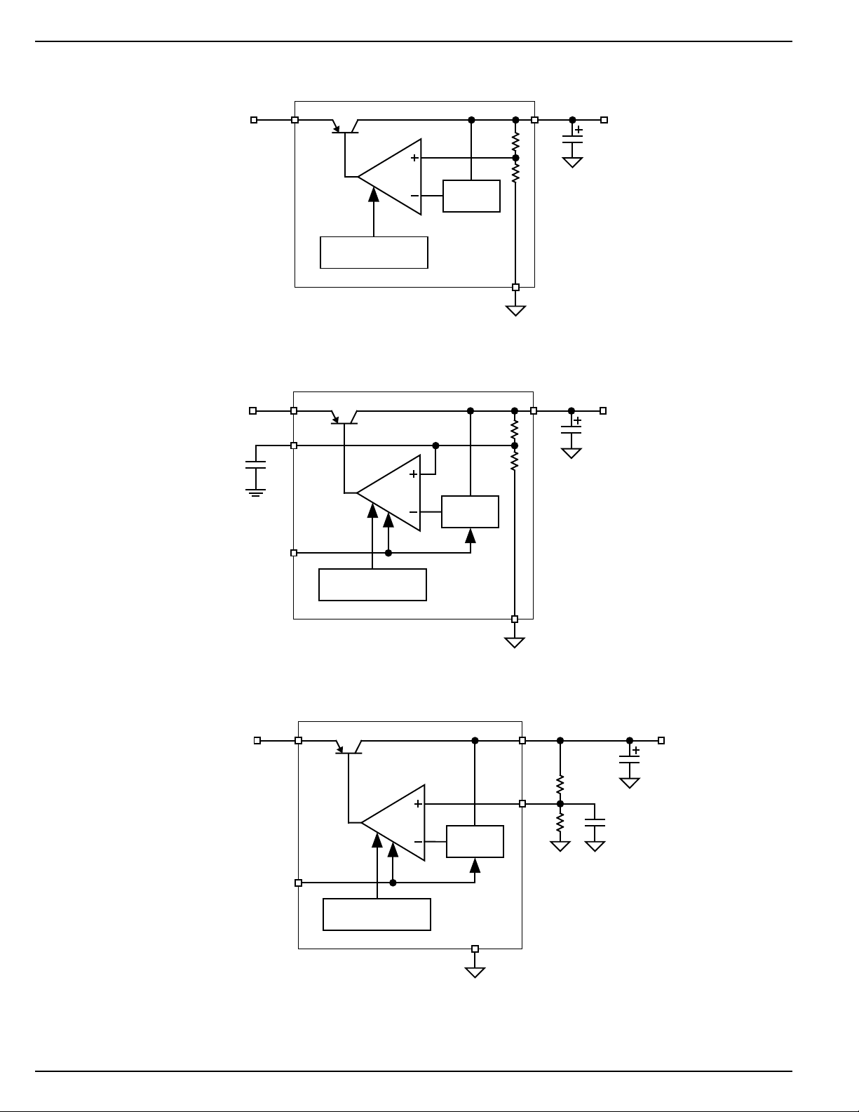
Block Diagrams
V
IN
V
IN
C
BYP
(optional)
IN
OUT
Bandgap
Ref.
Current Limit
Thermal Shutdown
MIC5207-x.xBZ
GND
Low-Noise Fixed Regulator (TO-92 version only)
IN
BYP
EN
Bandgap
Ref.
V
REF
OUT
V
OUT
C
OUT
V
OUT
C
OUT
Current Limit
Thermal Shutdown
MIC5207-x.xBM5
GND
Ultra-Low-Noise Fixed Regulator
V
IN
IN
Bandgap
Ref.
V
REF
EN
Current Limit
Thermal Shutdown
MIC5207BM5
GND
OUT
ADJ
R1
R2
C
C
BYP
(optional)
OUT
V
OUT
Ultra-Low-Noise Adjustable Regulator
MIC5207 6 January 2000
Page 7

MIC5207 Micrel
P =
T – T
D
(max)
J(max) A
JA
()
θ
Applications Information
Enable/Shutdown
Forcing EN (enable/shutdown) high (> 2V) enables the regulator. EN is compatible with CMOS logic gates.
If the enable/shutdown feature is not required, connect EN
(pin 3) to IN (supply input, pin 1). See Figure 1.
Input Capacitor
A 1µF capacitor should be placed from IN to GND if there is
more than 10 inches of wire between the input and the ac filter
capacitor or if a battery is used as the input.
Reference Bypass Capacitor
BYP (reference bypass) is connected to the internal voltage
reference. A 470pF capacitor (C
GND quiets this reference, providing a significant reduction in
output noise. C
when using C
reduces the regulator phase margin;
BYP
, output capacitors of 2.2µF or greater are
BYP
generally required to maintain stability.
The start-up speed of the MIC5207 is inversely proportional
to the size of the reference bypass capacitor. Applications
requiring a slow ramp-up of output voltage should consider
larger values of C
consider omitting C
. Likewise, if rapid turn-on is necessary,
BYP
.
BYP
If output noise is not a major concern, omit C
BYP open.
Output Capacitor
An output capacitor is required between OUT and GND to
prevent oscillation. The minimum size of the output capacitor
is dependent upon whether a reference bypass capacitor is
used. 1.0µF minimum is recommended when C
used (see Figure 2). 2.2µF minimum is recommended when
C
is 470pF (see Figure 1). Larger values improve the
BYP
regulator’s transient response. The output capacitor value
may be increased without limit.
The output capacitor should have an ESR (effective series
resistance) of about 5Ω or less and a resonant frequency
above 1MHz. Ultra-low-ESR capacitors can cause a low
amplitude oscillation on the output and/or underdamped
transient response. Most tantalum or aluminum electrolytic
capacitors are adequate; film types will work, but are more
expensive. Since many aluminum electrolytics have electrolytes that freeze at about –30°C, solid tantalums are recommended for operation below –25°C.
At lower values of output current, less output capacitance is
required for output stability. The capacitor can be reduced to
0.47µF for current below 10mA or 0.33µF for currents below
1mA.
No-Load Stability
The MIC5207 will remain stable and in regulation with no load
(other than the internal voltage divider) unlike many other
voltage regulators. This is especially important in CMOS
RAM keep-alive applications.
Thermal Considerations
The MIC5207 is designed to provide 180mA of continuous
current in a very small package. Maximum power dissipation
can be calculated based on the output current and the voltage
) connected from BYP to
BYP
and leave
BYP
BYP
is not
drop across the part. To determine the maximum power
dissipation of the package, use the junction-to-ambient thermal resistance of the device and the following basic equation:
T
is the maximum junction temperature of the die,
J(max)
125°C, and TA is the ambient operating temperature. θJA is
layout dependent; Table 1 shows examples of junction-toambient thermal resistance for the MIC5207.
Package
SOT-23-5 (M5) 235°C/W 170°C/W 130°C/W
θθ
θJA Recommended
θθ
Minimum Footprint Copper Clad
θθ
θJA 1" Square
θθ
θθ
θ
θθ
JC
Table 1. SOT-23-5 Thermal Resistance
The actual power dissipation of the regulator circuit can be
determined using the equation:
PD = (VIN – V
Substituting P
D(max)
) I
OUT
+ VIN I
GND
OUT
for PD and solving for the operating
conditions that are critical to the application will give the
maximum operating conditions for the regulator circuit. For
example, when operating the MIC5207-3.3BM5 at room
temperature with a minimum footprint layout, the maximum
input voltage for a set output current can be determined as
follows:
125˚C25˚C
P
P 425mW
D(max)
D(max)
=
=
−
235
The junction-to-ambient thermal resistance for the minimum
footprint is 220°C/W, from Table 1. The maximum power
dissipation must not be exceeded for proper operation. Using
the output voltage of 3.3V and an output current of 150mA,
the maximum input voltage can be determined. From the
Electrical Characteristics table, the maximum ground current
for 150mA output current is 3000µA or 3mA.
455mW = (VIN – 3.3V) 150mA + VIN·3mA
455mW = VIN·150mA – 495mW + VIN·3mA
920mW = VIN·153mA
V
IN(max)
= 6.01V
Therefore, a 3.3V application at 150mA of output current can
accept a maximum input voltage of 6V in a SOT-23-5 package. For a full discussion of heat sinking and thermal effects
on voltage regulators, refer to the Regulator Thermals section of Micrel’s
tors
handbook.
Designing with Low-Dropout Voltage Regula-
Low-Voltage Operation
The MIC5207-1.8 and MIC5207-2.5 require special consideration when used in voltage-sensitive systems. They may
momentarily overshoot their nominal output voltages unless
appropriate output and bypass capacitor values are chosen.
During regulator power up, the pass transistor is fully saturated for a short time, while the error amplifier and voltage
reference are being powered up more slowly from the output
January 2000 7 MIC5207
Page 8
MIC5207 Micrel
(see “Block Diagram”). Selecting larger output and bypass
capacitors allows additional time for the error amplifier and
reference to turn on and prevent overshoot.
To ensure that no overshoot is present when starting up into
a light load (100µA), use a 4.7µF output capacitance and
470pF bypass capacitance. This slows the turn-on enough to
allow the regulator to react and keep the output voltage from
exceeding its nominal value. At heavier loads, use a 10µF
output capacitance and 470pF bypass capacitance. Lower
values of output and bypass capacitance can be used,
depending on the sensitivity of the system.
Applications that can withstand some overshoot on the
output of the regulator can reduce the output capacitor and/
or reduce or eliminate the bypass capacitor. Applications that
are not sensitive to overshoot due to power-on reset delays
can use normal output and bypass capacitor configurations.
Please note the junction temperature range of the regulator
at 1.8V output (fixed and adjustable) is 0˚C to +125˚C.
Fixed Regulator Applications
MIC5207-x.xBM5
V
IN
15
2
3
V
OUT
2.2µF
4
470pF
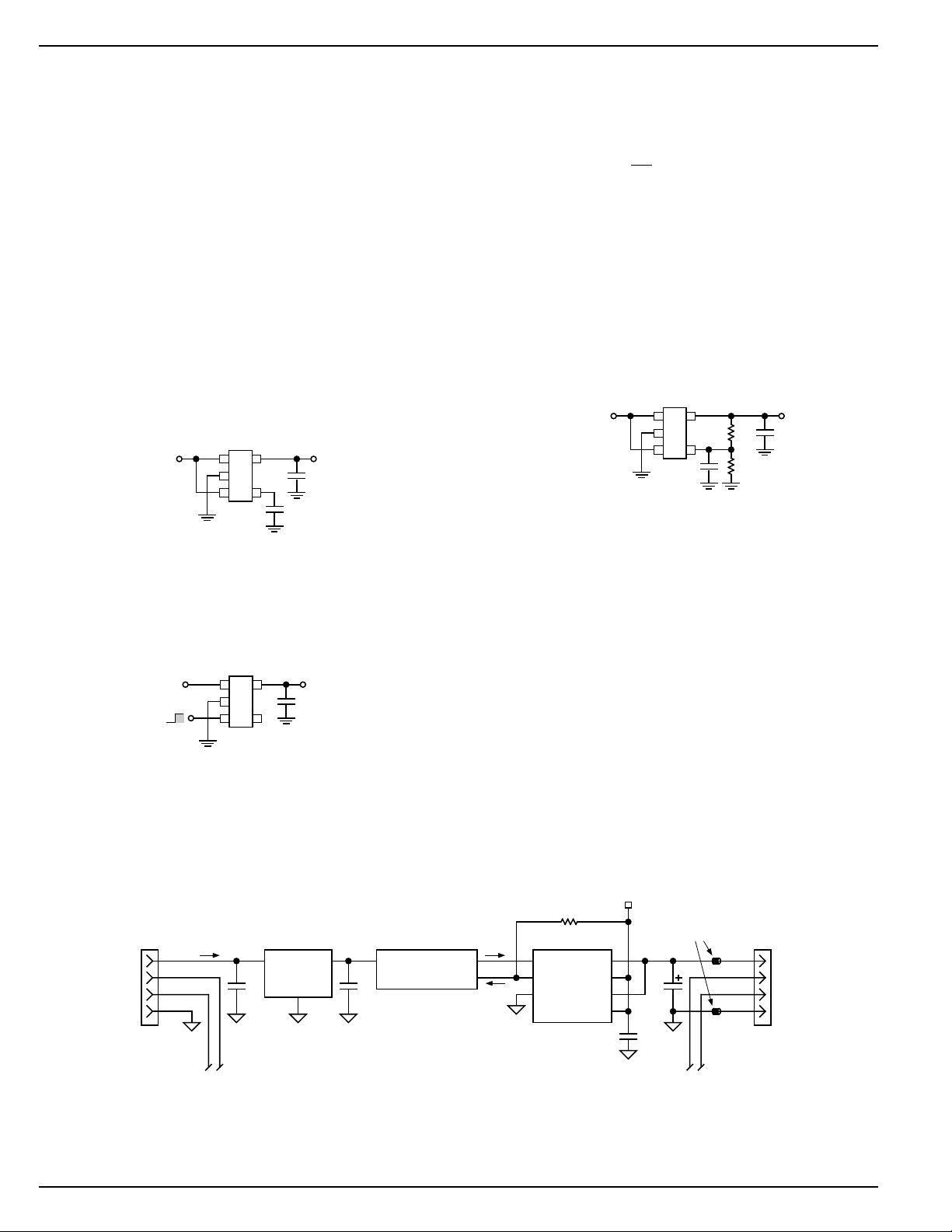
Figure 1. Ultra-Low-Noise Fixed Voltage Regulator
Figure 1 includes a 470pF capacitor for ultra-low-noise operation and shows EN (pin 3) connected to IN (pin 1) for an
application where enable/shutdown is not required. C
OUT
=
2.2µF minimum.
Enable
Shutdown
MIC5207-x.xBM5
V
IN
15
2
34
EN
V
OUT
1.0µF
Figure 2. Low-Noise Fixed Voltage Regulator
Adjustable Regulator Applications
The MIC5207BM5 can be adjusted to a specific output
voltage by using two external resistors (figure 3). The resistors set the output voltage based on the following equation:
R2
VV1
=+
OUT
REF REF
, V 1.242V
R1
=
This equation is correct due to the configuration of the
bandgap reference. The bandgap voltage is relative to the
output, as seen in the block diagram. Traditional regulators
normally have the reference voltage relative to ground;
therefore, their equations are different from the equation for
the MIC5207BM5.
Resistor values are not critical because ADJ (adjust) has a
high input impedance, but for best results use resistors of
470kΩ or less. A capacitor from ADJ to ground provides
greatly improved noise performance.
MIC5207BM5
V
IN
15
2
3
4
470pF
R1
R2
V
OUT
2.2µF
Figure 3. Ultra-Low-Noise
Adjustable Voltage Regulator
Figure 3 includes the optional 470pF noise bypass capacitor
from ADJ to GND to reduce output noise.
Dual-Supply Operation
When used in dual-supply systems where the regulator load
is returned to a negative supply, the output voltage must be
diode clamped to ground.
USB Application
Figure 4 shows the MIC5207-3.3BZ (3-terminal, TO-92) in a
USB application. Since the V
supply may be greater than
BUS
10 inches from the regulator, a 1µF input capacitor is included.
Figure 2 is an example of a basic low-noise configuration.
C
= 1µF minimum.
OUT
V
CC
5.0V
Upstream
V
BUS
100mA max.
V
D+
D–
GND
BUS
MIC5207-3.3BZ
IN OUT
1µF 1µF
Data
GND
ON/OFF
OVERCURRENT
10k
MIC2525USB Controller
EN OUT
FLG IN
GND OUT
0.1µF
Ferrite
Beads
V
BUS
D+
USB
D–
150µF
IN
GND
Data
Port
Figure 4. Single-Port Self-Powered Hub
MIC5207 8 January 2000
Page 9
MIC5207 Micrel
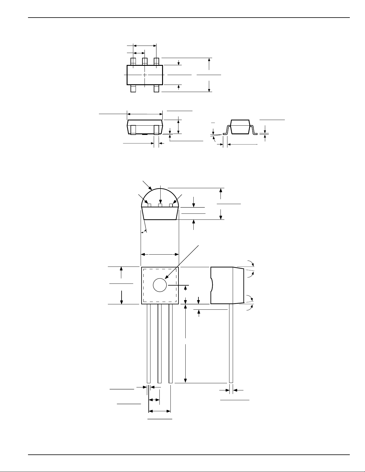
Package Information
1.90 (0.075) REF
0.95 (0.037) REF
3.02 (0.119)
2.80 (0.110)
0.50 (0.020)
0.35 (0.014)
0.090 (2.286) Radius, typ.
1
10° typ.
1.75 (0.069)
1.50 (0.059)
1.30 (0.051)
0.90 (0.035)
SOT-23-5 (M5)
2
BOTTOM VIEW
0.185 (4.699)
0.175 (4.445)
0.15 (0.006)
0.00 (0.000)
3
0.055 (1.397)
0.045 (1.143)
3.00 (0.118)
2.60 (0.102)
10°
0°
0.145 (3.683)
0.135 (3.429)
0.085 (2.159) Diam.
DIMENSIONS:
MM (INCH)
0.60 (0.024)
0.10 (0.004)
0.20 (0.008)
0.09 (0.004)
0.185 (4.699)
0.175 (4.445)
Seating Plane
0.016 (0.406)
0.014 (0.356)
0.055 (1.397)
0.045 (1.143)
5° typ.
0.090 (2.286) typ.
5° typ.
0.025 (0.635) Max
Uncontrolled
Lead Diameter
0.500 (12.70) Min.
0.0155 (0.3937)
0.0145 (0.3683)
0.105 (2.667)
0.095 (2.413)
TO-92 (Z)
January 2000 9 MIC5207
Page 10

MIC5207 Micrel
MIC5207 10 January 2000
Page 11

MIC5207 Micrel
January 2000 11 MIC5207
Page 12

MIC5207 Micrel
MICREL INC. 1849 FORTUNE DRIVE SAN JOSE, CA 95131 USA
TEL + 1 (408) 944-0800 FAX + 1 (408) 944-0970 WEB http://www.micrel.com
This information is believed to be accurate and reliable, however no responsibility is assumed by Micrel for its use nor for any infringement of patents or
other rights of third parties resulting from its use. No license is granted by implication or otherwise under any patent or patent right of Micrel Inc.
© 2000 Micrel Incorporated
MIC5207 12 January 2000
 Loading...