

Page 1
General Description
MIC4721
1.5A 2MHz Integrated Switch
Features
Buck Regulator
The Micrel MIC4721 is a high efficiency PWM buck (stepdown) regulators that provides up to 1.5A of output
current. The MIC4721 operates at 2MHz and has
proprietary internal compensation that allows a closed loop
bandwidth of over 200KHz.
The low on-resistance internal p-channel MOSFET of the
MIC4721 allows efficiencies up to 94%, reduces external
components count and eliminates the need for an
expensive current sense resistor.
The MIC4721 operates from 2.7V to 5.5V input and the
output can be adjusted down to 1V. The devices can
operate with a maximum duty cycle of 100% for use in lowdropout conditions.
The MIC4721 is available in the 10-pin MSOP package
with a junction operating range from –40°C to +125°C.
Data sheets and support documentation can be found on
Micrel’s web site at: www.micrel.com.
• 2.7 to 5.5V supply voltage
• 2MHz PWM mode
• Output current to 1.5A
• Up to 94% efficiency
• 100% maximum duty cycle
• Adjustable output voltage option down to 1V
• Ultra-fast transient response
• Ultra-small external components
Stable with a 1µH inductor and a 4.7µF output capacitor
• Fully integrated 1.5A MOSFET switch
• Micropower shutdown
• Power Good pin
• Thermal shutdown and current limit protection
• Pb-free 10-pin MSOP package
• –40°C to +125°C junction temperature range
Applications
• FPGA/DSP/ASIC applications
• General point of load
• Broadband communications
• DVD/TV recorders
• Point of sale
• Printers/Scanners
• Set top boxes
• Computing peripherals
• Video cards
___________________________________________________________________________________________________________
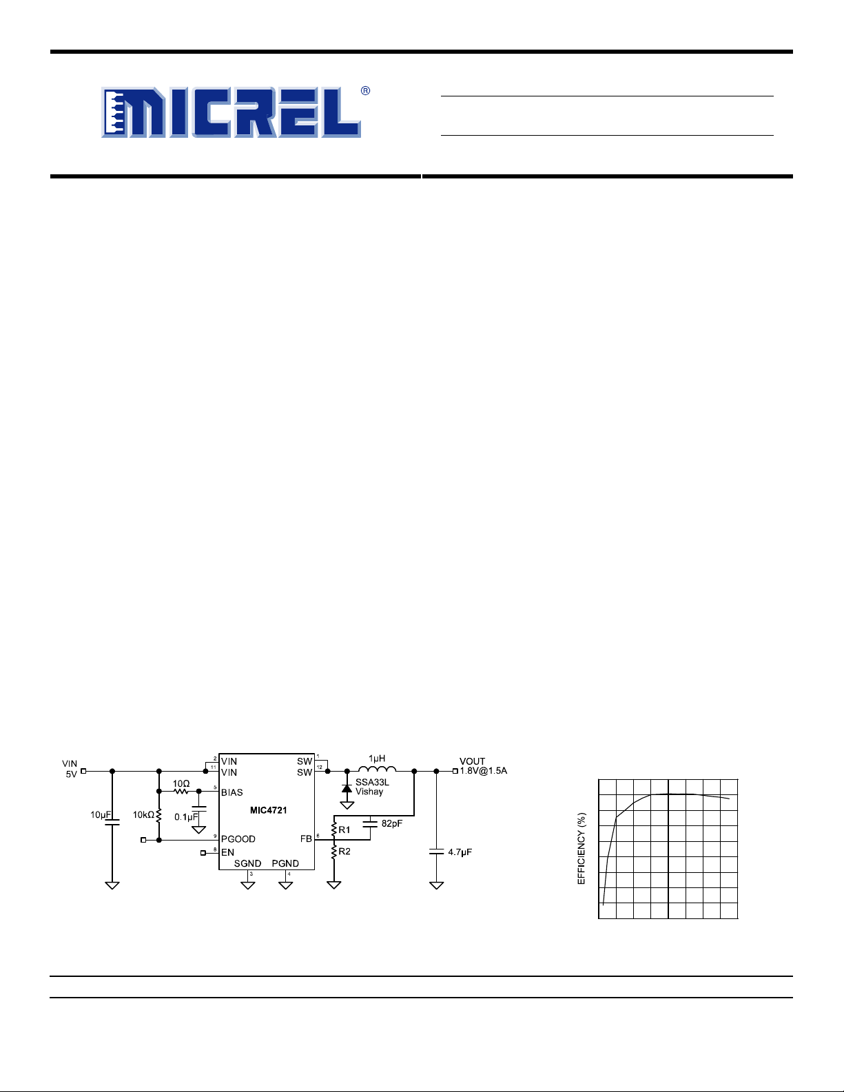
Typical Application
May 2007
1.5A 2MHz Buck Regulator
Micrel Inc. • 2180 Fortune Drive • San Jose, CA 95131 • USA • tel +1 (
5VIN to 3.3VO Efficiency
94
92
90
88
86
84
82
408
) 944-0800 • fax + 1 (408) 474-1000 • http://www.micrel.com
80
78
76
0 0.2 0.4 0.6 0.8 1.2 1.4 1.6
OUTPUT CURRENT (A)
1.0
1
M9999-052907-A
Page 2

Micrel, Inc. MIC4721
Ordering Information
Part Number Voltage Temperature Range Package Lead Finish
MIC4721YMM Adj. –40° to +125°C 10-Pin MSOP Pb-Free
Pin Configuration
Pin Description
Pin Number Pin Name Pin Function
1, 10 SW Switch (Output): Internal power P-Channel MOSFET output switch.
2, 9 VIN
3 SGND
4 BIAS
5 FB
6 EN
7 PGOOD
8 PGND Power Ground. Provides the ground return path for the high-side drive current.
10 SW
9
VIN
8
PGND
7
PGOOD
VIN
SGND
BIAS
FB EN65
1SW
2
3
4
10-Pin MSOP (MM)
Supply Voltage (Input): Supply voltage for the source of the internal P-channel
MOSFET and driver.
Requires bypass capacitor to GND.
Signal (Analog) Ground. Provides return path for control circuitry and internal
reference.
Internal circuit bias supply. Must be bypassed with a 0.1µF ceramic capacitor to
SGND.
Feedback. Input to the error amplifier, connect to the external resistor divider
network to set the output voltage.
Enable (Input). Logic level low will shutdown the device, reducing the current
draw to less than 5µA.
Power Good. Open drain output that is pulled to ground when the output voltage
is within ±7.5% of the set regulation voltage.
May 2007
2
M9999-052907-A
Page 3

Micrel, Inc. MIC4721
Absolute Maximum Ratings
(1)
Operating Ratings
(2)
Supply Voltage (VIN).......................................................+6V
Output Switch Voltage (V
Output Switch Current (I
Logic Input Voltage (V
Storage Temperature (T
)..........................................+6V
SW
)............................................11A
SW
) ..................................–0.3V to VIN
EN
).........................–60°C to +150°C
s
Supply Voltage (VIN).....................................+2.7V to +5.5V
Logic Input Voltage (V
Junction Temperature (T
).......................................0V to VIN
EN
) ........................–40°C to +125°C
J
Junction Thermal Resistance
MSOP-10L (θ
MSOP-10L (θ
)...............................................130°C/W
JA
) ................................................43°C/W
JC
Electrical Characteristics
V
= VEN = 3.6V; L = 1µH; C
IN
Parameter Condition Min Typ Max Units
Supply Voltage Range
Under-Voltage Lockout
Threshold
UVLO Hysteresis 100 mV
Quiescent Current VFB = 0.9 * V
Shutdown Current VEN = 0V 2
[Adjustable] Feedback
Voltage
FB pin input current 1 nA
Current Limit in PWM Mode VFB = 0.9 * V
Output Voltage Line
Regulation
Output Voltage Load
Regulation
Maximum Duty Cycle
PWM Switch ON-
Resistance
Oscillator Frequency
Enable Threshold
Enable Hysteresis 50 mV
Enable Input Current 0.1
Power Good Range ±7 ±10 %
Power Good Resistance I
Over-Temperature
Shutdown
Over-Temperature
Hysteresis
Notes:
1. Exceeding the absolute maximum rating may damage the device.
2. The device is not guaranteed to function outside its operating rating.
3. Specification for packaged product only.
(3)
= 4.7µF; TA = 25°C, unless noted. Bold values indicate –40°C< TJ < +125°C.
OUT
2.7 5.5
(turn-on)
2.45
(not switching) 570
NOM
2.55
2.65
900
10
± 2% (over temperature) I
3.5 5 A
NOM
V
> 2V; VIN = V
OUT
V
< 2V; VIN = 2.7V to 5.5V; I
OUT
20mA < I
V
≤ 0.4V
FB
I
= 50mA; VFB = 0.7V
SW
< 3A 0.2 %
LOAD
+500mV to 5.5V; I
OUT
FB_NOM
= 100mA
LOAD
= 100mA
LOAD
= 100mA
LOAD
(High Side Switch)
0.98
0.07 %
100
%
95
1.8
0.5
2
0.85
1.02
200
300
2.2
1.3
2.3
= 500µA 145
PGOOD
250
160
20
V
V
µA
µA
V
mΩ
mΩ
MHz
V
µA
Ω
°C
°C
May 2007
3
M9999-052907-A
Page 4
Micrel, Inc. MIC4721
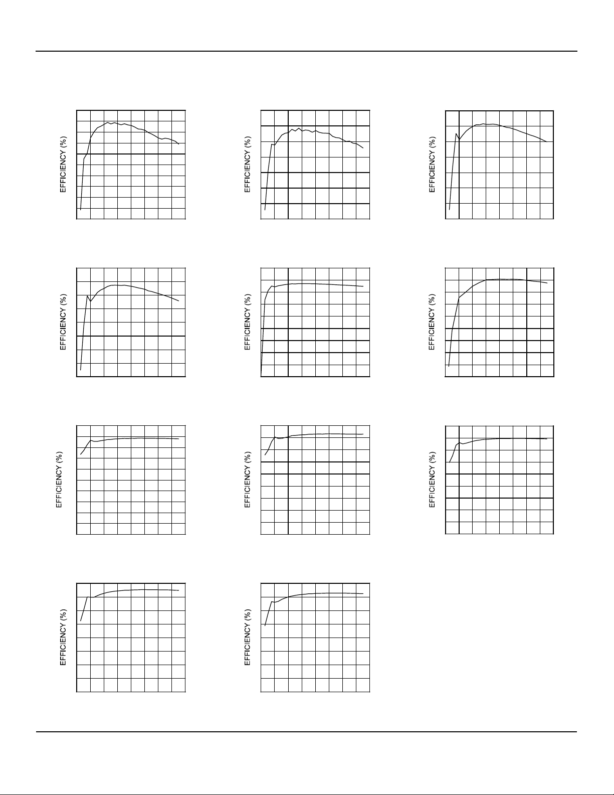
Typical Characteristics
3.3VIN to 2.5VO Efficiency
94
93
92
91
90
89
88
87
86
85
84
0 0.2 0.4 0.6 0.8 1.2 1.4 1.6
OUTPUT CURRENT (A)
1.0
3.3VIN to 1.2VO Efficiency
82
80
78
76
74
72
70
68
66
0 0.2 0.4 0.6 0.8 1.2 1.4 1.6
OUTPUT CURRENT (A)
1.0
5VIN to 2.5VO Efficiency
100
90
80
70
60
50
40
30
20
10
0
0 0.2 0.4 0.6 0.8 1.2 1.4 1.6
OUTPUT CURRENT (A)
1.0
5VIN to 1.2VO Efficiency
80
70
60
50
40
30
20
10
0
0 0.2 0.4 0.6 0.8 1.2 1.4 1.6
OUTPUT CURRENT (A)
1.0
3.3VIN to 1.8VO Efficiency
90
88
86
84
82
80
78
76
0 0.2 0.4 0.6 0.8 1.2 1.4 1.6
OUTPUT CURRENT (A)
1.0
3.3VIN to 1VO Efficiency
90
80
70
60
50
40
30
20
10
0
0 0.2 0.4 0.6 0.8 1.0 1.2 1.4 1.6
OUTPUT CURRENT (A)
5VIN to 1.8VO Efficiency
90
80
70
60
50
40
30
20
10
0
0 0.2 0.4 0.6 0.8 1.2 1.4 1.6
OUTPUT CURRENT (A)
1.0
3.3VIN to 1.5VO Efficiency
86
84
82
80
78
76
74
72
0 0.2 0.4 0.6 0.8 1.2 1.4 1.6
OUTPUT CURRENT (A)
1.0
5VIN to 3.3VO Efficiency
94
92
90
88
86
84
82
80
78
76
0 0.2 0.4 0.6 0.8 1.2 1.4 1.6
OUTPUT CURRENT (A)
1.0
5VIN to 1.5VO Efficiency
90
80
70
60
50
40
30
20
10
0
0 0.2 0.4 0.6 0.8 1.2 1.4 1.6
OUTPUT CURRENT (A)
1.0
5VIN to 1VO Efficiency
80
70
60
50
40
30
20
10
0
0 0.2 0.4 0.6 0.8 1.2 1.4 1.6
OUTPUT CURRENT (A)
1.0
May 2007
4
M9999-052907-A
Page 5
Micrel, Inc. MIC4721
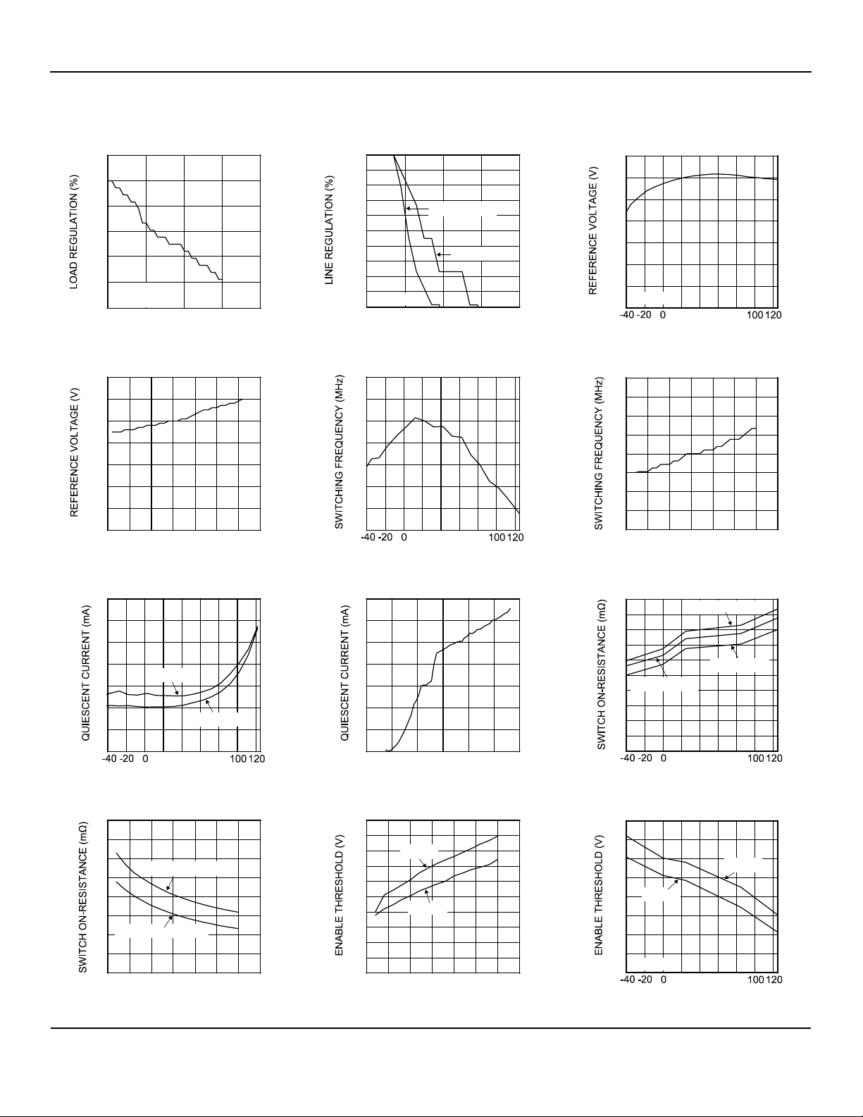
Typical Characteristics
Load Regulation
0.02
0.00
-0.02
-0.04
-0.06
-0.08
VO = 1.8V
= 3.3V
V
IN
-0.10
0 0.5 1.0 1.5 2.0
OUTPUT CURRENT (A)
Reference Voltage
1.002
1.001
1.000
0.999
0.998
0.997
0.996
0.995
vs. Input Voltage
2.5 3 3.5 4 4.5 5 5.5 6
INPUT VOLTAGE (V)
Quiescent Current
3.5
3.0
2.5
2.0
1.5
1.0
0.5
vs. Temperature
VIN = 2.5V
0
TEMPERATURE (°C)
VIN = 3.3V
20 40 60 80
Switch On-Resistance
180
170
160
150
140
130
120
110
100
vs. Input Voltage
RON @ I
RON @ I
2.5 3 3.5 4 4.5 5 5.5 6
INPUT VOLTAGE (V)
OUT
OUT
= 0.1A
= 1.5A
Line Regulation
0.000
-0.005
-0.010
-0.015
-0.020
-0.025
-0.030
-0.035
-0.040
-0.045
VO = 1.8V
-0.050
23456
I
= 100mA
OUT
I
= 1.5A
OUT
INPUT VOLTAGE (V)
1.005
1.000
0.995
0.990
0.985
0.980
0.975
0.970
Switching Frequency
2.04
2.02
2.00
1.98
1.96
1.94
1.92
1.90
vs. Temperature
20 40 60 80
TEMPERATURE (°C)
2.20
2.15
2.10
2.05
2.00
1.95
1.90
1.85
1.80
Quiescent Current
vs. Input Voltage
1.4
1.2
1.0
0.8
0.6
0.4
0.2
0
0123456
INPUT VOLTAGE (V)
Enable Threshold
1.10
1.05
1.00
0.95
0.90
0.85
0.80
0.75
0.70
0.65
0.60
vs. Input Voltage
Turn-on
Turn-off
2.5 3 3.5 4 4.5 5 5.5 6
INPUT VOLTAGE (V)
1.00
0.95
0.90
0.85
0.80
0.75
0.70
0.65
0.60
Reference Voltage
vs. Temperature
VIN = 3.3V
20 40 60 80
TEMPERATURE (°C)
Switching Frequency
vs. Input Voltage
2.5 3 3.5 4 4.5 5 5.5 6
INPUT VOLTAGE (V)
Switch On-Resistance
200
180
160
140
120
100
vs. Temperature
RON @ 3.3V
80
60
40
20
0
TEMPERATURE (°C)
RON @ 2.7V
RON @ 5V
IN
20 40 60 80
IN
Enable Threshold
vs. Temperature
Turn-on
Turn-off
VIN = 3.3V
20 40 60 80
TEMPERATURE (°C)
IN
May 2007
5
M9999-052907-A
Page 6
Micrel, Inc. MIC4721
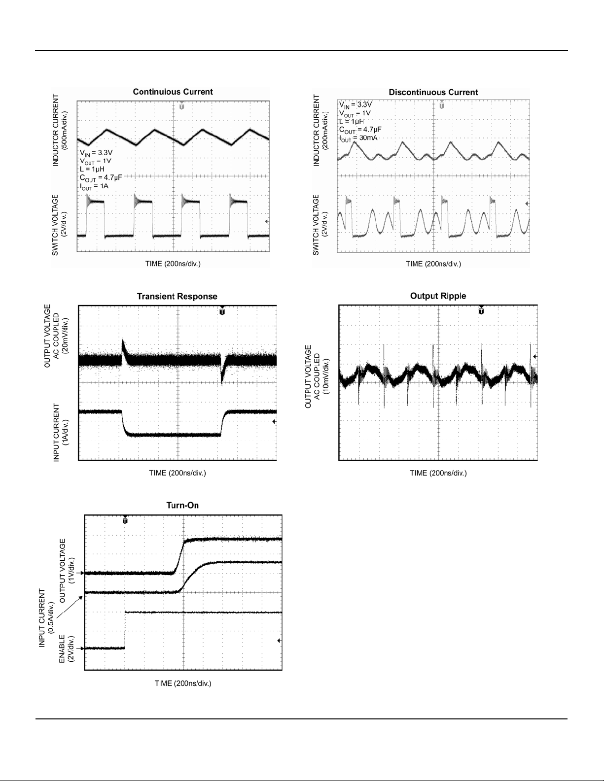
Functional Characteristics
May 2007
6
M9999-052907-A
Page 7
Micrel, Inc. MIC4721
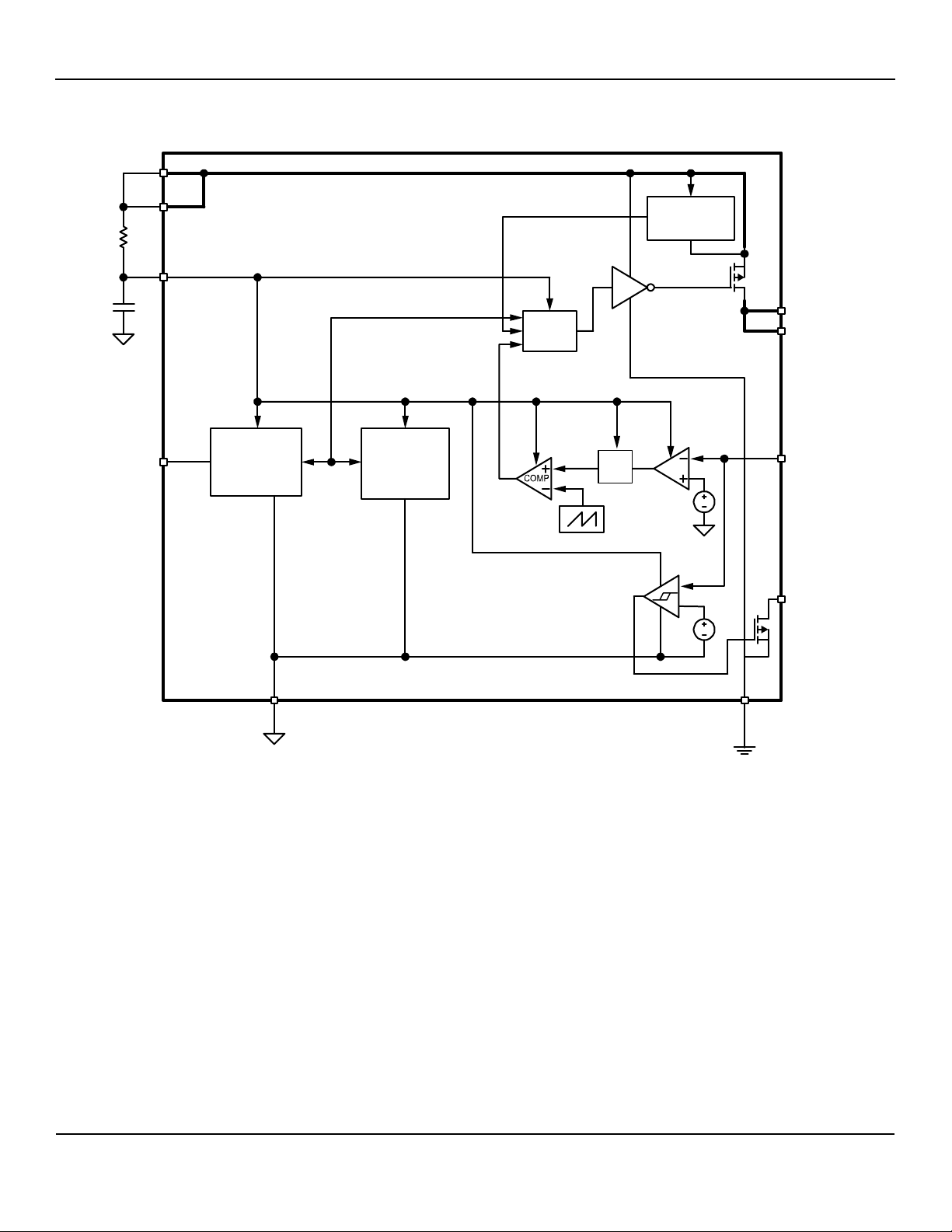
Functional Diagram
VIN
VIN
P-Channel
Current Limit
BIAS
HSD
PWM
Control
SW
SW
Bias,
UVLO,
Thermal
Shutdown
MIC4721 Block Diagram
Soft
Start
EA
1.0V
1.0V
FB
PGOOD
PGND
EN
Enable and
Control Logic
SGND
May 2007
7
M9999-052907-A
Page 8

Micrel, Inc. MIC4721
Pin Descriptions
VIN
Two pins for VIN provide power to the source of the
internal P-channel MOSFET along with the current
limiting sensing. The VIN operating voltage range is from
2.7V to 5.5V. Due to the high switching speeds, a 10µF
capacitor should be placed close to VIN and power
ground (PGND) at each pin for bypassing. Please refer
to the section on layout recommendations.
BIAS
The bias (BIAS) provides power to the internal reference
and control sections of the MIC4721. A 10Ω resistor
from VIN to BIAS and a 0.1µF from BIAS to SGND is
required.
EN
The enable pin provides a logic level control of the
output. At a low level, the output is shut off and supply
current at the VIN pin is greatly reduced (typically <2µA).
A high level turns the output on. The enable pin must not
be driven above the supply voltage.
FB
The feedback pin (FB) connects to the negative input of
the internal error amplifier. The pin is connected to an
external resistor divider, which sets the output voltage.
A feedforward capacitor across the upper resistor in the
divider is recommended for most designs. To reduce
current draw, a 10K feedback resistor is recommended
from the output to the FB pin (R1). The large resistor
value and the parasitic capacitance of the FB pin can
cause a high frequency pole that can reduce the overall
system phase margin. By placing a feedforward
capacitor, these effects can be significantly reduced.
SW
The switch (SW) pin connects directly to the inductor
and provides the switching current necessary to operate
in PWM mode. Due to the high speed switching on this
pin, the switch node should be routed away from
sensitive nodes. This pin also connects to the cathode of
the free-wheeling diode.
PGOOD
The power good pin pulls low to indicate the output
voltage is within its regulation range. When power good
is low, then the output voltage is within ±10% of the set
regulation voltage. For output voltages greater or less
than 10%, the PGOOD pin is high. This should be
connected to the input supply through a pull up resistor.
A delay can be added by placing a capacitor from
PGOOD-to-ground.
PGND
Power ground (PGND) is the ground path for the
MOSFET drive current. The current loop for the power
ground should be as small as possible and separate
from the Signal ground (SGND) loop. Refer to the
section on layout recommendations for more details.
SGND
Signal ground (SGND) is the ground path for the biasing
and control circuitry. The current loop for the signal
ground should be separate from the power ground
(PGND) loop. Refer to the section on layout
recommendations for more details.
May 2007
8
M9999-052907-A
Page 9
Micrel, Inc. MIC4721
(
−
Application Information
The MIC4721 is a 1.5A PWM non-synchronous buck
regulator. A regulated DC output voltage is obtained by
switching an input voltage supply, and filtering the
switched voltage through an inductor and capacitor.
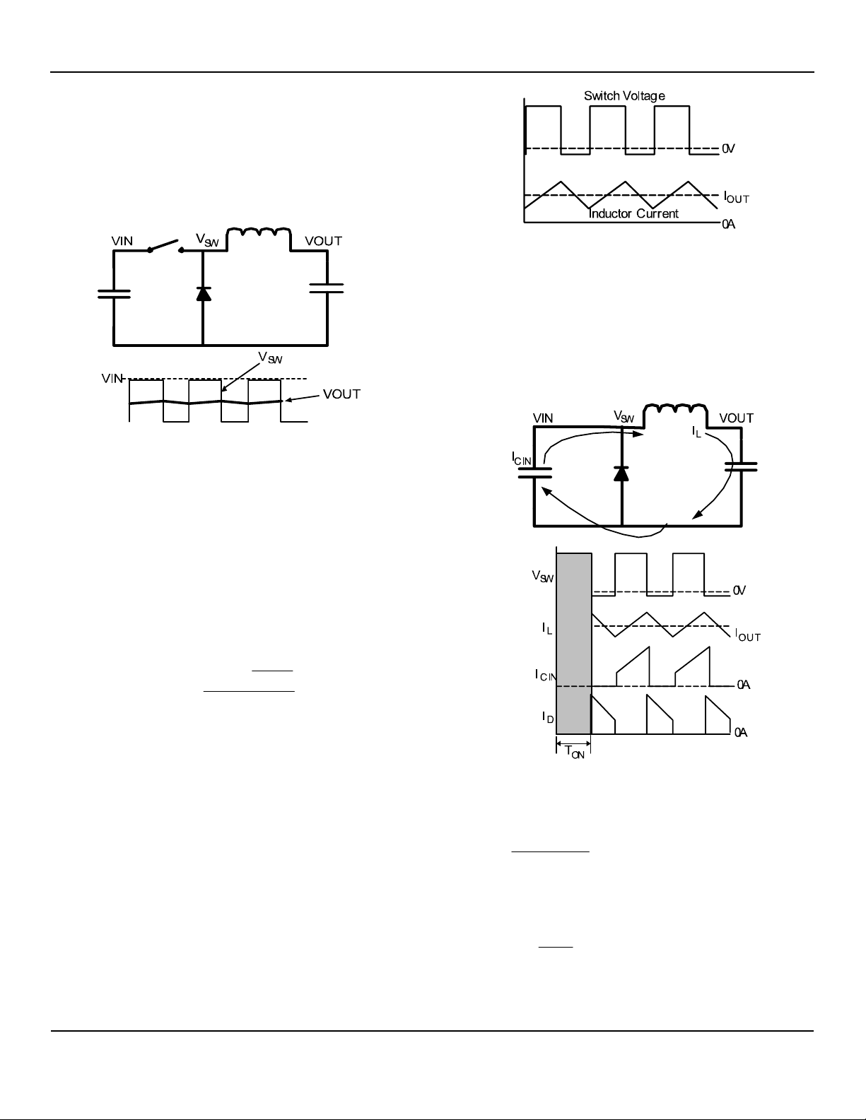
Figure 1 shows a simplified example of a non-synchronous buck converter and its input/output voltage.
Figure 2. Continuous Operation
The output voltage is regulated by pulse width
modulating (PWM) the switch voltage to the average
required output voltage. The switching can be broken up
into two cycles; On and Off.
As seen in Figure 3, the high side switch is turned on
(on-time) and current flows from the input supply through
the inductor and to the output.
Figure 1. Simplified Buck Converter
For a non-synchronous buck converter, there are two
modes of operation; continuous and discontinuous. The
mode refers to the state of current in the inductor. If
current continuously flows through the inductor
throughout the switching cycle, it is in continuous
operation. If the inductor current drops to zero during the
off time, it is in discontinuous operation. Critically
continuous is the point where any decrease in output
current will cause it to enter discontinuous operation.
The critically continuous load current can be calculated
as follows.
2
V
OUT
−
V
IN
fL
××
2
S
Where: f
V
OUT
I
_
CRITICALOUT
is the switching frequency (2MHz for the
S
=
MIC4721).
L is the output inductance (Henry).
When I
is less than I
OUT
OUT_CRITICAL
, the buck converter
operates in discontinuous mode and the inductor current
goes to zero before the end of each switching cycle.
When I
is greater than I
OUT
OUT_CRITICAL
, the converter
operates in continuous mode and current always flows in
the inductor. Continuous or discontinuous operation
determines how peak inductor current is calculated.
Continuous Operation
Figure 2 illustrates the switch voltage and inductor
current during continuous operation.
Figure 3. On-Time
The inductor current is charged at the rate:
)
VV
OUTIN
L
To determine the total on-time, or time at which the
inductor charges, the duty cycle needs to be calculated.
The duty cycle can be calculated as:
V
OUT
D =
V
IN
and the On time is:
May 2007
9
M9999-052907-A
Page 10
Micrel, Inc. MIC4721
Ton =
D
f
S
therefore, peak to peak ripple current is:
()
VV
×−
OUTIN
II
+=
−
OUTPKPK
Lf
×
S
V
OUT
V
IN
Discontinuous Operation
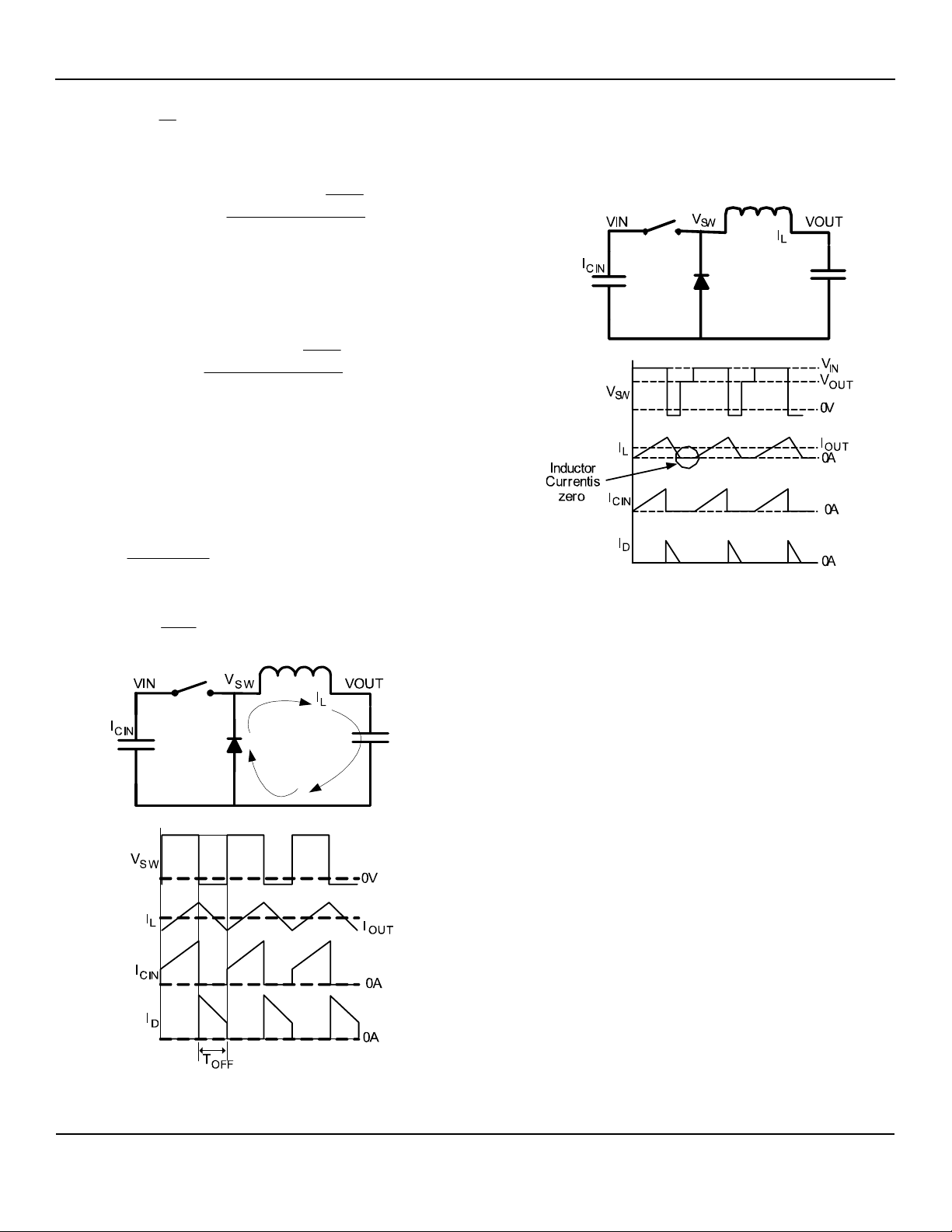
Discontinuous operation is when the inductor current
discharges to zero at sometime during the off cycle.
Figure 5 demonstrates the switch voltage and inductor
currents during discontinuous operation.
Peak-to-peak ripple current is used in calculating output
voltage ripple.
The peak current (or maximum inductor current) is equal
to the output current plus ½ the peak-to-peak current.
V
()
VV
OUTIN
II
+=
OUTPK
2
OUT
×−
V
IN
Lf
××
S
The peak inductor current is used when selecting a
suitable output inductor.
Figure 4 demonstrates circuit activity during the off-time.
When the high-side internal P-channel MOSFET turns
off, current must flow through the free-wheeling diode,
since inductor current must remain continuous. In this
case, the inductor discharge rate is:
()
+
VV
−
The total off time can be calculated as:
Toff
DOUT
L
Figure 5. Discontinuous Operation
D
−
1
=
f
S
When the inductor current (IL) has completely
discharged, the voltage on the switch node rings at the
frequency determined by the parasitic capacitance and
the inductor value. In figure 5, it is drawn as a DC
voltage, but to see actual operation (with ringing) refer to
the functional characteristics.
Discontinuous mode of operation has the advantage
over full PWM in that at light loads, the MIC4721 will skip
pulses as necessary, reducing gate drive losses,
drastically improving light load efficiency.
May 2007
Duty Cycle Considerations
The P-Channel MOSFET inside the MIC4721 allows the
FET to remain in the on-state indefinitely (100% duty
cycle). This feature is useful for maintaining output
voltage regulation in battery powered and other
applications where the input voltage drops close to the
output voltage.
When the MOSFET is operating at the 2MHz switching
frequency, the maximum operating duty cycle is typically
82%. In situations where a duty cycle greater than the
maximum operating duty cycle is required, the MIC4721
will keep the FET turned on for additional cycles to
maintain output voltage regulation. This effectively
decreases the switching frequency, allowing a larger
duty cycle. The output voltage ripple increases slightly
Figure 4. Off-Time
when the MIC4721 is in pulse skipping mode.
10
M9999-052907-A
Page 11
Micrel, Inc. MIC4721
Efficiency Considerations
Calculating the efficiency is as simple as measuring
power out and dividing it by the power in.
P
Efficiency
Where input power (P
P
= VIN × IIN
IN
and output power (P
P
= V
OUT
OUT
P
IN
) is:
IN
) is calculated as:
OUT
× I
OUT
OUT
100×=
type of material used, approximating core losses
becomes very difficult, so verify inductor temperature
rise.
Switching losses
occur twice each cycle, when the
switch turns on and when the switch turns off. This is
caused by a non-ideal world where switching transitions
are not instantaneous, and neither are current
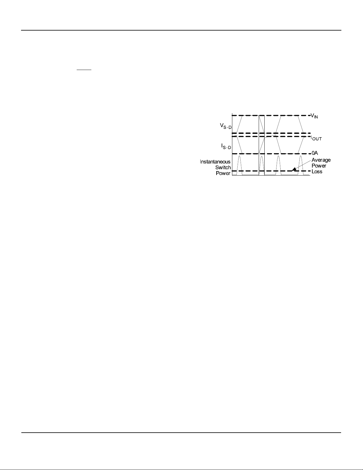
transitions. Figure 6 demonstrates (or exaggerates…)
how switching losses due to the transitions dissipate
power in the switch.
The Efficiency of the MIC2207 is determined by several
factors.
• R
(Internal P-channel Resistance)
DSON
• Diode conduction losses
• Inductor Conduction losses
• Switching losses
R
losses
DSON
the high side P-channel MOSFET. The amount of power
loss can be approximated by:
P
Where D is the duty cycle.
Since the MIC4721 uses an internal P-channel
MOSFET, R
supply voltage. Higher supply voltage yields a higher
gate to source voltage, reducing the R
reducing the MOSFET conduction losses. A graph
showing typical R
found in the typical characteristics section of this
datasheet.
Diode conduction losses
voltage drop (VF) and the output current. Diode power
losses can be approximated as follows:
P
For this reason, the low forward voltage drop Schottky
diode is the rectifier of choice. The low forward voltage
drop will help reduce diode conduction losses, and
improve efficiency. Duty cycle, or the ratio of output
voltage to input voltage, determines whether the
dominant factor in conduction losses will be the internal
MOSFET or the Schottky diode. Higher duty cycles
place the power losses on the high side switch, and
lower duty cycles place the majority of power loss on the
Schottky diode.
Inductor conduction losses
multiplying the DC resistance (DCR) times the square of
the output current:
are caused by the current flowing through
SW
= R
DSON
losses are inversely proportional to
DSON
DSON
2
× I
OUT
× D
vs. input supply voltage can be
occur due to the forward
= VF × I
D
× (1 – D)
OUT
(PL) can be calculated by
PL = DCR × I
OUT
2
DSON
, thus
Figure 6. Switching Transition Losses
Normally, when the switch is on, the voltage across the
switch is low (virtually zero) and the current through the
switch is high. This equates to low power dissipation.
When the switch is off, voltage across the switch is high
and the current is zero, again with power dissipation
being low. During the transitions, the voltage across the
switch (VS-D) and the current through the switch (IS-D)
are at midpoint of their excursions and cause the
transition to be the highest instantaneous power point.
During continuous mode, these losses are the highest.
Also, with higher load currents, these losses are higher.
For discontinuous operation, the transition losses only
occur during the “off” transition since the “on” transitions
there is no current flow through the inductor.
Component Selection
Input Capacitor
A 10µF ceramic is recommended on each VIN pin for
bypassing. X5R or X7R dielectrics are recommended for
the input capacitor. Y5V dielectrics lose most of their
capacitance over temperature and voltage and are
therefore not recommended. Also, tantalum and
electrolytic capacitors alone are not recommended
because of their reduced RMS current handling,
reliability, and higher ESR. Smaller case size capacitors
are recommended due to their lower ESL (equivalent
series inductance). Please refer to layout
recommendations for proper layout of the input
capacitors.
Also, be aware that there are additional core losses
associated with switching current in an inductor. Since
most inductor manufacturers do not give data on the
May 2007
11
M9999-052907-A
Page 12
Micrel, Inc. MIC4721
Output Capacitor
The MIC4721 is designed for a 4.7µF output capacitor.
X5R or X7R dielectrics are recommended for the output
capacitor. Y5V dielectrics lose most of their capacitance
over temperature and voltage and are therefore, not
recommended. Smaller case size capacitors are
recommended due to their lower ESL. The MIC4721
utilizes type III voltage mode internal compensation and
utilizes an internal zero to compensate for the double
pole roll off of the LC filter. For this reason, larger output
capacitors can create instabilities. In cases where a
4.7µF output capacitor is not sufficient, the MIC2208
offers the ability to externally control the compensation,
allowing for a wide range of output capacitor types and
values.
calculated by:
VR
×
1
R
=
2
FB
VV
−
FBOUT
Feedforward Capacitor (CFF)
A capacitor across the resistor from the output to the
feedback pin (R1) is recommended for most designs.
This capacitor can give a boost to phase margin and
increase the bandwidth for transient response. Also,
large values of feedforward cap acitance can slow down
the turn-on characteristics, reducing inrush current. For
maximum phase boost, C
C
=
FF
π
can be calculated as follows:
FF
1
12002
RKHz
××
Inductor Selection
The MIC4721 is designed for use with a 1µH inductor.
Proper selection should ensure the inductor can handle
the maximum RMS and peak currents required by the
load. Maximum current ratings of the inductor are
generally given in two methods; permissible DC current
and saturation current. Permissible DC current can be
rated either for a 40°C temperature rise or a 10% to 20%
loss in inductance. Ensure the inductor selected can
handle the maximum operating current. When saturation
current is specified, make sure that there is enough
margin that the peak current since at higher
temperatures, the inductor will saturate at a lower
current.
Diode Selection
Since the MIC4721 is non-synchronous, a free-wheeling
diode is required for proper operation. A Schottky diode
is recommended due to the low forward voltage drop
and fast reverse recovery time. The diode should be
rated to handle the average output current. Also, the
reverse voltage rating of the diode should exceed the
maximum input voltage. Please refer to the layout
recommendations to minimize switching noise.
Feedback Resistors
The feedback resistor set the output voltage by dividing
down the output and sending it to the feedback pin. The
feedback voltage is 1.0V. Calculating the set output
voltage is as follows:
R
⎛
VV
⎜
FBOUT
⎝
Where R1 is the resistor from V
⎞
+= 1
⎟
21R
⎠
to FB and R2 is the
OUT
resistor from FB to GND.
The recommended feedback resistor values for common
output voltages are available in the bill of materials at the
end of this specification. Although the resistance range
of the FB resistors is very wide, R1 is recommended to
be 10K. This minimizes the effect the parasitic
capacitance of the FB node. Resistor R2 can be
May 2007
Bias filter
A small 10Ω resistor is recommended from the input
supply to the bias pin along with a small 0.1µF ceramic
capacitor from bias-to-ground. This will bypass the high
frequency noise generated by the violent switching of
high currents from reaching the internal reference and
control circuitry. Tantalum and electrolytic capacitors are
not recommended since these types of capacitors aren’t
as effective at filtering high frequencies.
Loop Stability and Bode Analysis
Bode analysis is an excellent way to measure small
signal stability and loop response in power supply
designs. Bode analysis monitors gain and phase of a
control loop. This is done by breaking the feedback loop
and injecting a signal into the feedback node and
comparing the injected signal to the output signal of the
control loop. This will require a network analyzer to
sweep the frequency and compare the injected signal to
the output signal. The most common method of injection
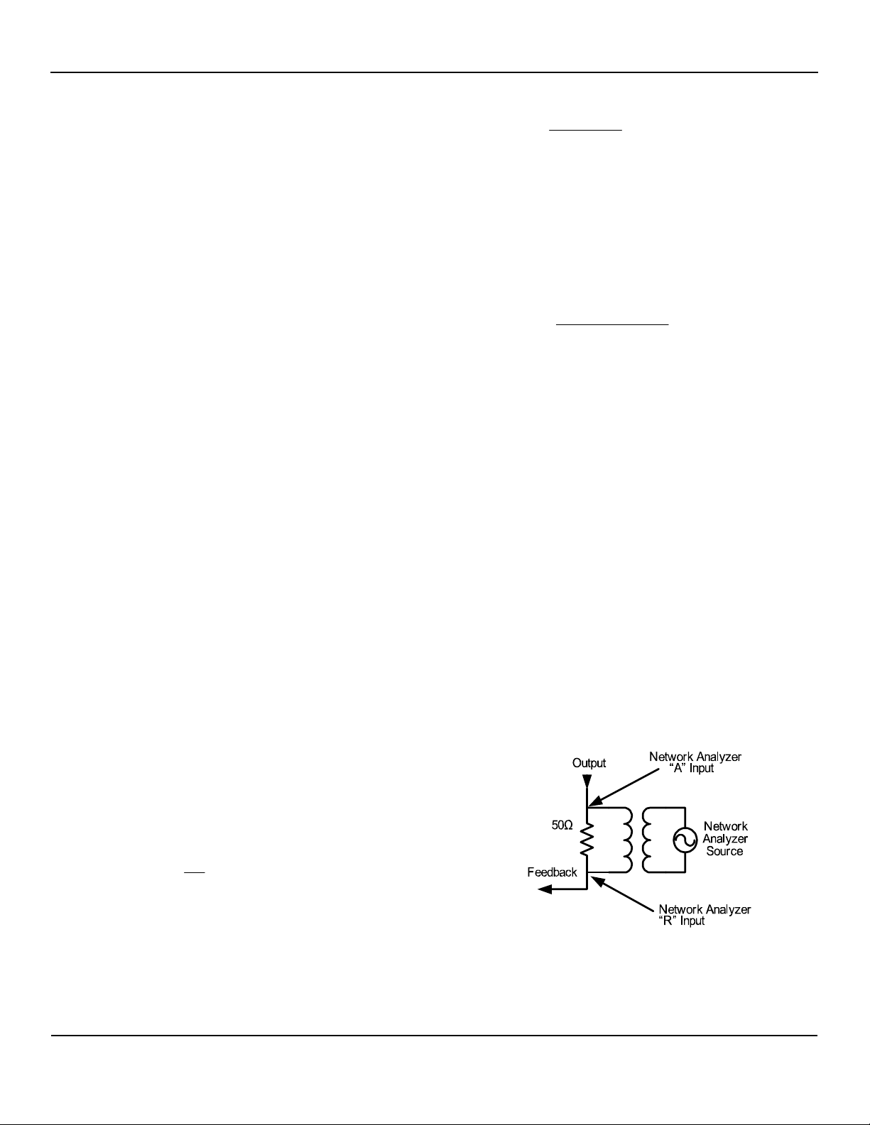
is the use of a transformer. Figure 7 demonstrates how a
transformer is used to inject a signal into the feedback
network.
Figure 7. Transformer Injection
A 50Ω resistor allows impedance matching from the
network analyzer source. This method allows the DC
loop to maintain regulation and allow the network
analyzer to insert an AC signal on top of the DC voltage.
12
M9999-052907-A
Page 13
Micrel, Inc. MIC4721
The network analyzer will then sweep the source while
monitoring A and R for an A/R measurement. While this
is the most common method for measuring the gain and
phase of a power supply, it does have significant
limitations. First, to measure low frequency gain and
phase, the transformer needs to be high in inductance.
This makes frequencies <100Hz require an extremely
large and expensive transformer. Conversely, it must be
able to inject high frequencies. Transformers with these
wide frequency ranges generally need to be custom
made and are extremely expensive (usually to the tune
of several hundred dollars!). By using an op-amp, cost
and frequency limitations caused by an injection
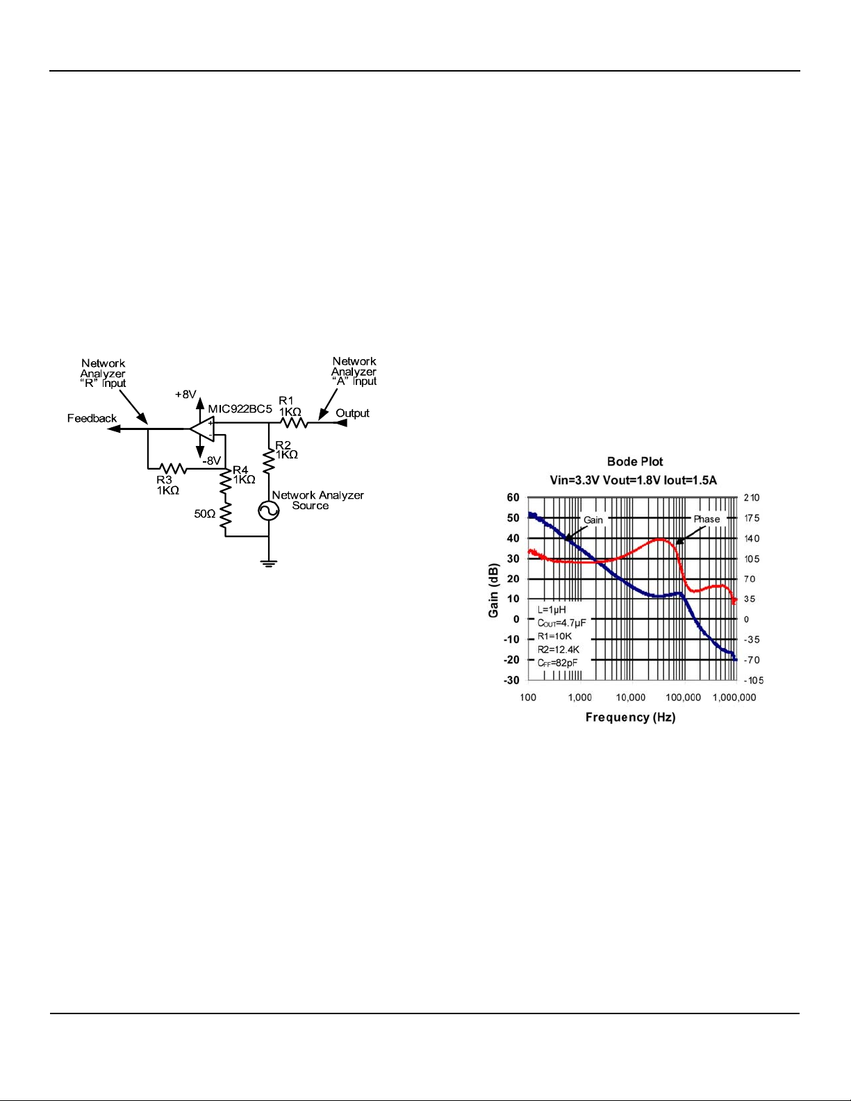
transformer are completely eliminated. Figure 8
demonstrates using an op-amp in a summing amplifier
configuration for signal injection.
R channels. Remember to always measure the output
voltage with an oscilloscope to ensure the measurement
is working properly. You should see a single sweeping
sinusoidal waveform without distortion on the output. If
there is distortion of the sinusoid, reduce the amplitude
of the source signal. You could be overdriving the
feedback causing a large signal response.
The following Bode analysis show the small signal loop
stability of the MIC4721. The MIC4721 utilizes a type III
compensation. This is a dominant low frequency pole,
followed by 2 zero’s and finally the double pole of the
inductor capacitor filter, creating a final 20dB/decade roll
off. Bode analysis gives us a few important data points;
speed of response (Gain Bandwidth or GBW) and loop
stability. Loop speed or GBW determines the response
time to a load transient. Faster response times yield
smaller voltage deviations to load steps. Instability in a
control loop occurs when there is gain and positive
feedback. Phase margin is the measure of how stable
the given system is. It is measured by determining how
far the phase is from crossing zero when the gain is
equal to 1 (0dB).
Figure 8. Op Amp Injection
R1 and R2 reduce the DC voltage from the output to the
non-inverting input by half. The network analyzer is
generally a 50Ω source. R1 and R2 also divide the AC
signal sourced by the network analyzer by half. These
two signals are “summed” together at half of their
original input. The output is then amplified by 2 by R3
and R4 (the 50Ω is to balance the network analyzer’s
source impedance) and sent to the feedback signal. This
essentially breaks the loop and injects the AC signal on
top of the DC output voltage and sends it to the
feedback. By monitoring the feedback “R” and output
“A”, gain and phase are measured. This method has no
minimum frequency. Ensure that the bandwidth of the
op-amp being used is much greater than the expected
bandwidth of the power supply’s control loop. An op-amp
with >100MHz bandwidth is more than sufficient for most
power supplies (which includes both linear and
switching) and are more common and significantly
cheaper than the injection transformers previously
mentioned. The one disadvantage to using the op-amp
injection method; is the supply voltages need to be
below the maximum operating voltage of the op-amp.
Also, the maximum output voltage for driving 50Ω inputs
using the MIC922 is 3V. For measuring higher output
voltages, a 1M input impedance is required for the A and
May 2007
Typically for 3.3V
and 1.8V
IN
at 1.5A;
OUT
• Phase Margin = 47 Degrees
• GBW = 156KHz
Gain will also increase with input voltage. The following
graph shows the increase in GBW for an increase in
supply voltage.
13
M9999-052907-A
Page 14
Micrel, Inc. MIC4721
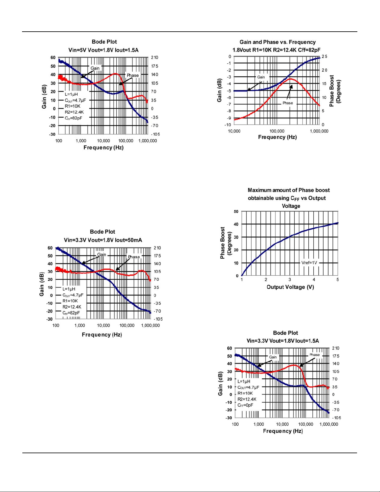
5V
and 1.8V
IN
at 1.5A load;
OUT
• Phase Margin = 43.1 Degrees
• GBW = 218KHz
The graph above shows the effects on the gain and
phase of the system caused by feedback resistors and a
feedforward capacitor. The maximum amount of phase
boost achievable with a feedforward capacitor is
graphed below.
The non-synchronous MIC4721 regulator only has the
ability to source current. This means that the regulator
must rely on the load to sink current. Th is causes a no nlinear response at light loads. The following plot shows
the effects of the pole created by the nonlinearity of the
output drive during light load (discontinuous) conditions.
3.3V
and 1.8V
IN
OUT IOUT
= 50mA;
• Phase Margin = 90.5 Degrees
• GBW = 64.4KHz
Feed Forward Capacitor
The feedback resistors are a gain reduction block in the
overall system response of the regulator. By placing a
capacitor from the output to the feedback pin, high
frequency signal can bypass the resistor divider, causing
a gain increase up to unity gain.
May 2007
By looking at the graph, phase margin can be affected to
a greater degree with higher output voltages. The next
bode plot shows the phase margin of a 1.8V output at
1.5A without a feedforward capacitor.
14
M9999-052907-A
Page 15
Micrel, Inc. MIC4721
As one can see the typical phase margin, using the
same resistor values as before without a feedforward
capacitor results in 33.6 degrees of phase margin. Our
prior measurement with a feedforward capacitor yielded
a phase margin of 47 degrees. The feedforward
capacitor has given us a phase boost of 13.4 degrees
(47 degrees – 33.6 Degrees = 13.4 Degrees).
Output Impedance and Transient Response
Output impedance, simply stated, is the amount of
output voltage deviation vs. the load current deviation.
The lower the output impedance, the better.
V
∆
Z
OUT
OUT
=
I
∆
OUT
V
and peak to peak current:
V
The following graph shows output impedance vs
frequency at 2A load current sweeping the AC current
from 10Hz to 10MHz, at 1A peak-to-peak amplitude.
dBm
10 ×Ω××=∆mW
10
dBm
10
=∆
10
2501
707.
mW
R
×
707.
LOAD
×Ω××
2501
Output impedance for a buck regulator is the parallel
impedance of the output capacitor and the MOSFET and
inductor divided by the gain:
XDCRR
++
LDSON
Z ||
TOTAL
=
GAIN
X
COUT
To measure output impedance vs. frequency, the load
current must be swept across the frequencies measured,
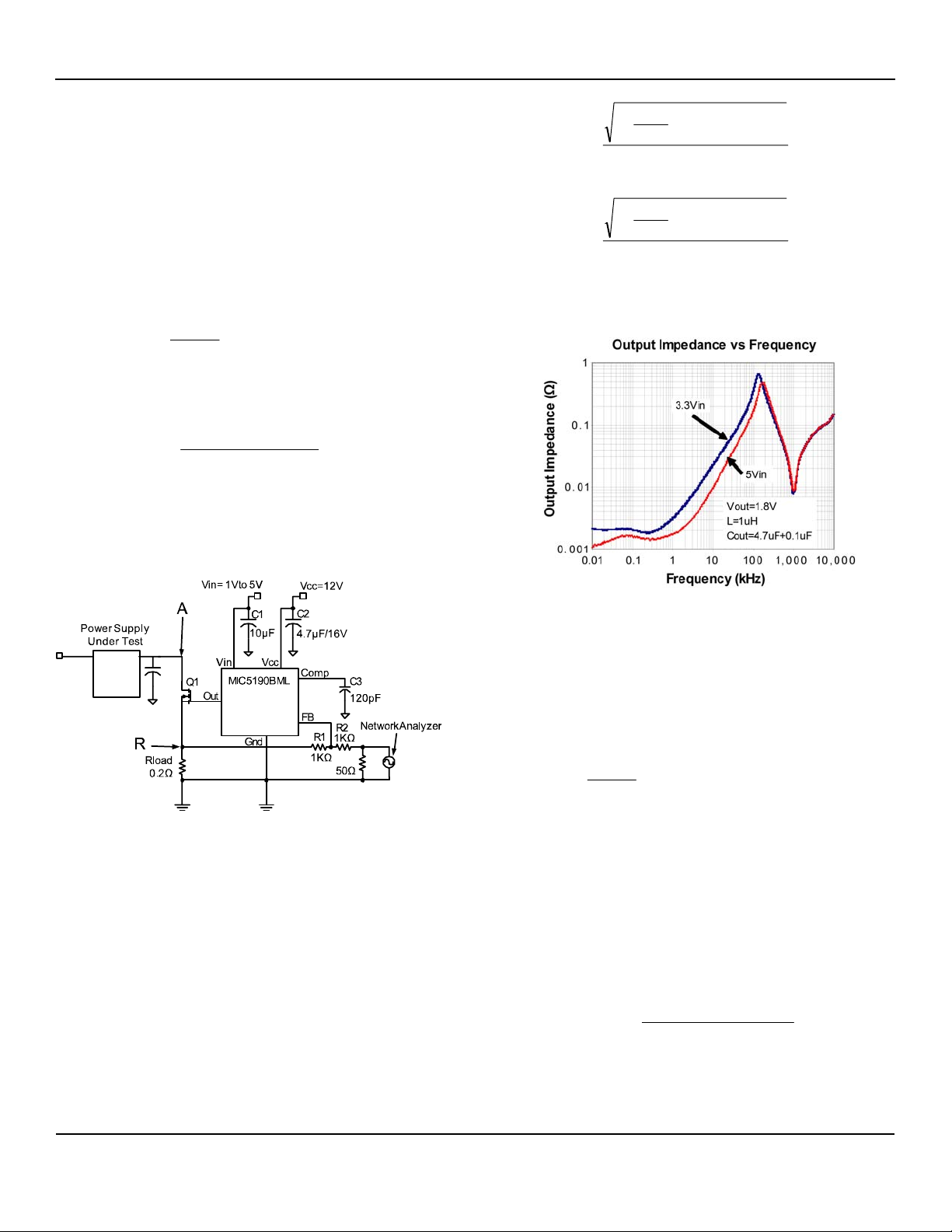
while the output voltage is monitored. Figure 9 shows a
test set-up to measure output impedance from 10Hz to
1MHz using the MIC5190 high speed controller.
Figure 9. Output Impedance Measurement
By setting up a network analyzer to sweep the feedback
current, while monitoring the output of the voltage
regulator and the voltage across the load resistance,
output impedance is easily obtainable. To keep the
current from being too high, a DC offset needs to be
applied to the network analyzer’s source signal. This can
be done with an external supply and 50Ω resistor. Make
sure that the currents are verified with an oscilloscope
first, to ensure the integrity of the signal measurement. It
is always a good idea to monitor the A and R
measurements with a scope while you are sweeping it.
To convert the network analyzer data from dBm to
something more useful (such as peak to peak voltage
and current in our case):
From this graph, you can see the effects of bandwidth
and output capacitance. For frequencies <200KHz, the
output impedance is dominated by the gain and
inductance. For frequencies >200KHz, the output
impedance is dominated by the capacitance. A good
approximation for transient response can be calculated
from determining the frequency of the load step in amps
per second:
f =
sec/A
π
2
Then, determine the output impedance by looking at the
output impedance vs frequency graph. Next, calculate
the voltage deviation times the load step;
∆V
OUT
= ∆I
OUT
×Z
OUT
The output impedance graph shows the relationship
between supply voltage and output impedance. This is
caused by the lower R
of the high side MOSFET
DSON
and the increase in gain with increased supply voltages.
This explains why higher supply voltages have better
transient response.
++↓
XDCRR
TOTAL
=↓
↑
GAIN
Z ||
LDSON
X
COUT
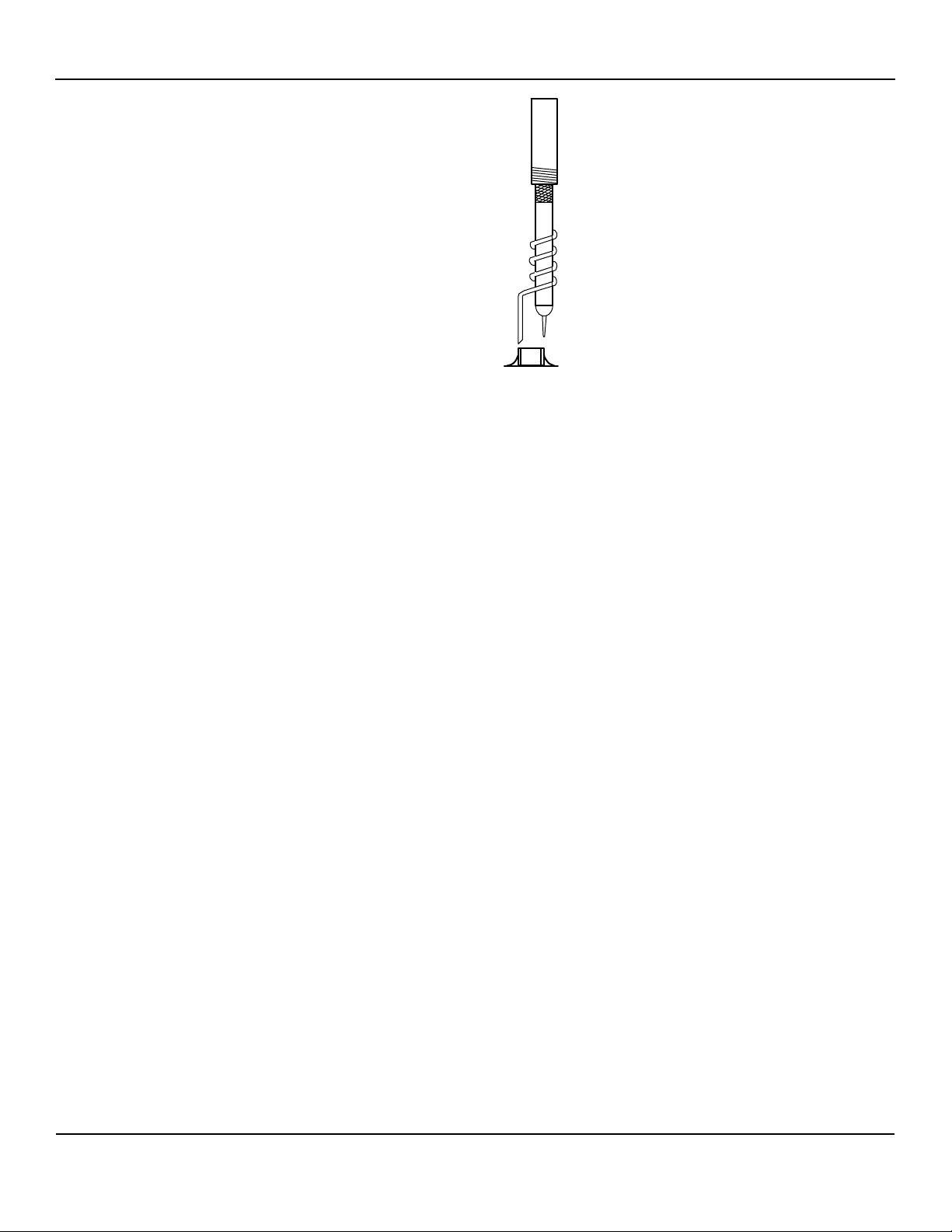
To properly measure ripple on either input or output of a
switching regulator, a proper ring in tip measurement is
required. Standard oscilloscope probes come with a
grounding clip, or a long wire with an alligator clip.
May 2007
15
M9999-052907-A
Page 16
Micrel, Inc. MIC4721
Unfortunately, for high frequency measurements, this
ground clip can pick-up high frequency noise and
erroneously inject it into the measured output ripple.
The standard evaluation board accommodates a home
made version by providing probe points for both the
input and output supplies and their respective grounds.
This requires the removing of the oscilloscope probe
sheath and ground clip from a standard oscilloscope
probe and wrapping a non-shielded bus wire around the
oscilloscope probe. If there does not happen to be any
non-shielded bus wire immediately available, the leads
from axial resistors will work. By maintaining the shortest
possible ground lengths on the oscilloscope probe, true
ripple measurements can be obtained.
May 2007
16
M9999-052907-A
Page 17
Micrel, Inc. MIC4721
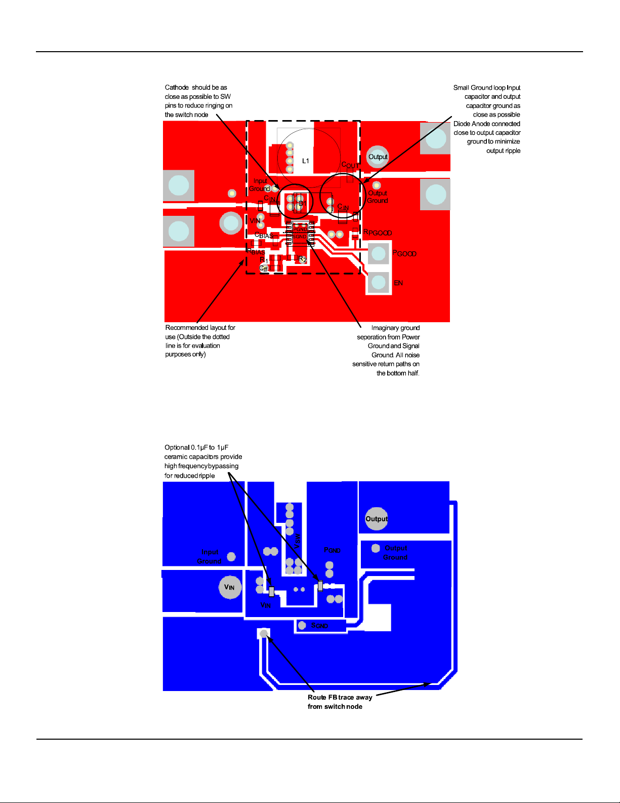
Recommended Layout MIC4721 1.5A Evaluation Board
Top
May 2007
Bottom
17
M9999-052907-A
Page 18
Micrel, Inc. MIC4721
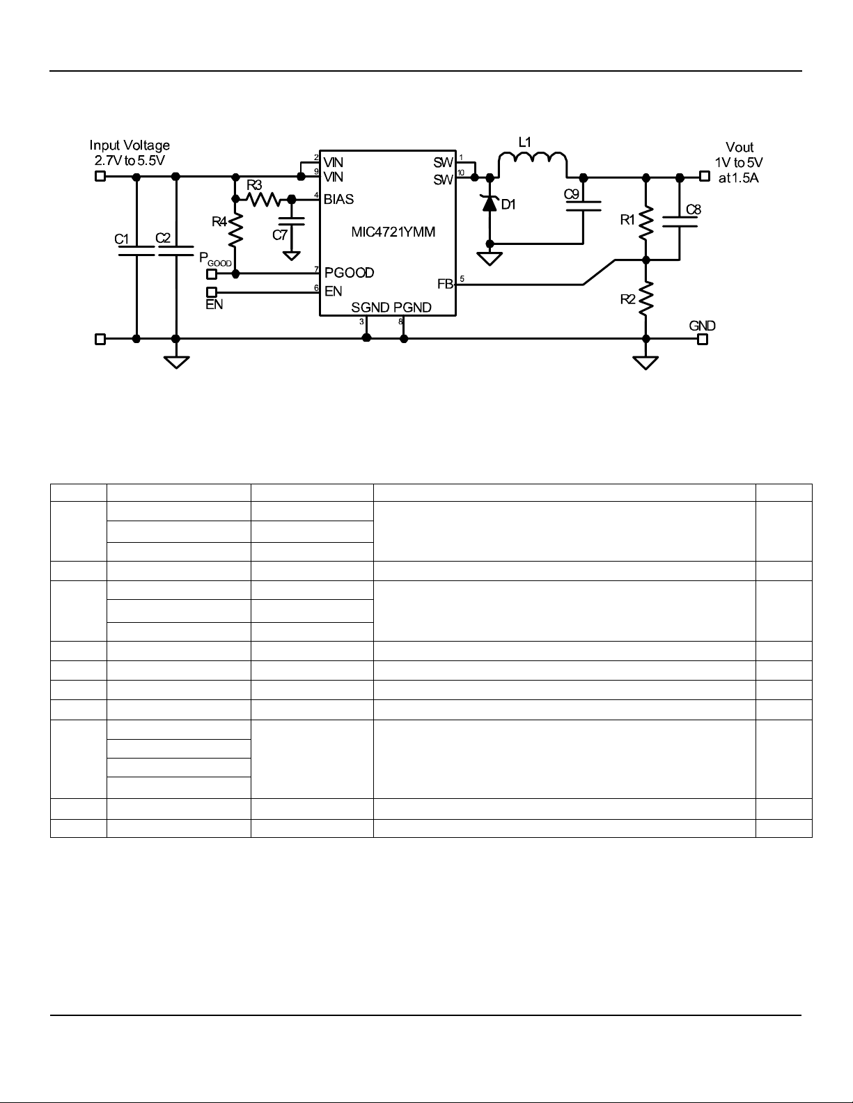
MIC4721 Schematic and B.O.M. for 1.5A Output
Bill of Materials
Item Part Number Manufacturer Description Qty.
C2012JB0J106K TDK
C1, C2
GRM219R60J106KE19 Murata
08056D106MAT AVX
C7
0402ZD104MAT AVX
C2012JB0J475K TDK
C9
GRM188R60J475KE19 Murata
06036D475MAT AVX
C8
D1
L1
R1, R4
VJ0402A820KXAA Vishay VT
SSA33L Vishay Semi
IHLP2525AH-01 1 Vishay Dale
CRCW04021002F Vishay Dale
CRCW04026651F
R2
CRCW04021242F
CRCW04022002F
Vishay Dale
CRCW04024022F
R3
CRCW040210R0F Vishay Dale
U1 MIC4721YMM Micrel, Inc.
Notes:
1. TDK: www.tdk.com
2. Murata: www.murata.com
3. AVX: www.avx.com
4. Vishay: www.vishay.com
5. Micrel, Inc.: www.micrel.com
(1)
(2)
(3)
(3)
(1)
(2)
(3)
(4)
(4)
(4)
(4)
(4)
(4)
(5)
1.5 2MHz Integrated Switch Buck Regulator 1
1µH Inductor 17.5mΩ(L)6.47mm x (W)6.86mm x (H)1.8mm 1
10µF Ceramic Capacitor X5R 0805 6.3V 2
0.1µF Ceramic Capacitor X5R 0402 10V 1
4.7µF Ceramic Capacitor X5R 0603 6.3V 1
82pF Ceramic Capacitor 0402 1
3A Schottky 30V SMA 1
10KΩ1% 0402 resistor 2
6.65 kΩ 1% 0402 For 2.5V
12.4 kΩ 1% 0402 For 1.8 V
20 kΩ 1% 0402 For 1.5 V
40.2 kΩ 1% 0402 For 1.2 V
Open For 1.0 V
OUT
OUT
OUT
OUT
OUT
10Ω 1% 0402 resistor 1
1
May 2007
18
M9999-052907-A
Page 19
Micrel, Inc. MIC4721
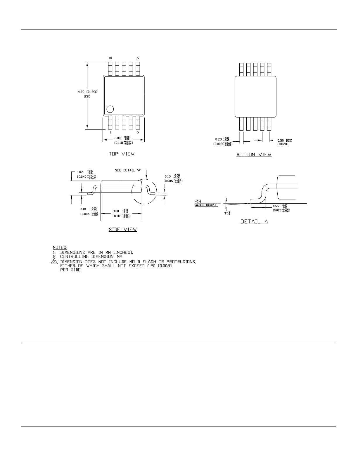
Package Information
10-Pin MSOP (MM)
MICREL, INC. 2180 FORTUNE DRIVE SAN JOSE, CA 95131 USA
TEL +1 (408) 944-0800 FAX +1 (408) 474-1000 WEB http://www.micrel.com
The information furnished by Micrel in this data sheet is believed to be accurate and reliable. However, no responsibility is assumed by Micrel for its
Micrel Products are not designed or authorized for use as components in life support appliances, devices or systems where malfunction of a product
can reasonably be expected to result in personal injury. Life support devices or systems are devices or systems that (a) are intended for surgical implant
into the body or (b) support or sustain life, and whose failure to perform can be reasonably expected to result in a significant injury to the user. A
Purchaser’s use or sale of Micrel Products for use in life support appliances, devices or systems is a Purchaser’s own risk and Purchaser agrees to fully
May 2007
use. Micrel reserves the right to change circuitry and specifications at any time without notification to the customer.
indemnify Micrel for any damages resulting from such use or sale.
© 2007 Micrel, Incorporated.
19
M9999-052907-A
 Loading...