

Page 1
MIC4467/4468/4469 Micrel
MIC4467/4468/4469
Quad 1.2A-Peak Low-Side MOSFET Driver
Bipolar/CMOS/DMOS
General Description
The MIC4467/8/9 family of 4-output CMOS buffer/drivers is
an expansion from the earlier single- and dual-output drivers,
to which they are functionally closely related. Because package pin count permitted it, each driver has been equipped
with a 2-input logic gate for added flexibility. Placing four highpower drivers in a single package also improves system
reliability and reduces total system cost. In some applications, one of these drivers can replace not only two packages
of single-input drivers, but some of the associated logic as
well.
Although primarily intended for driving power MOSFETs, and
similar highly capacitive loads, these drivers are equally well
suited to driving any other load (capacitive, resistive, or
inductive), which requires a high-efficiency, low-impedance
driver capable of high peak currents, rail-to-rail voltage swings,
and fast switching times. For example, heavily loaded clock
lines, coaxial cables, and piezoelectric transducers can all be
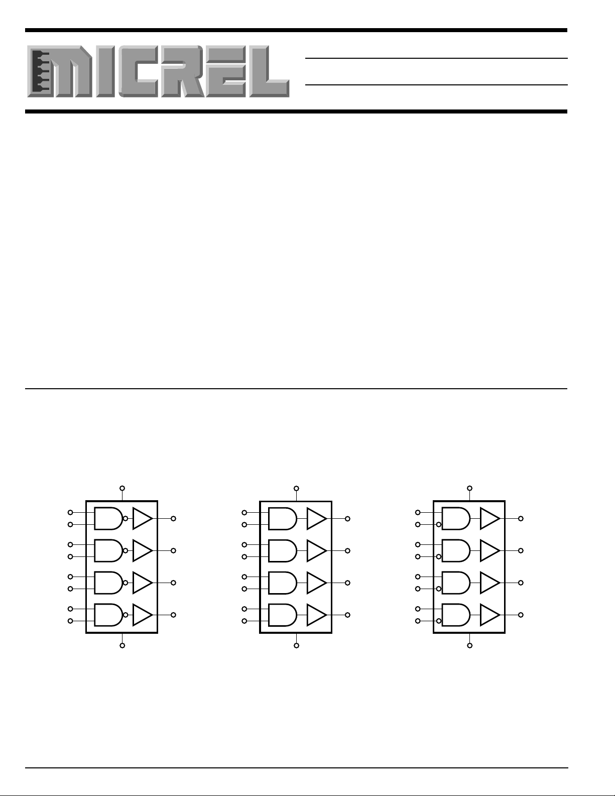
Logic Diagrams
Features
• Built using reliable, low power CMOS processes
• Latchproof. Withstands 500mA Inductive Kickback
• 3 Input Logic Choices
• Symmetrical Rise and Fall Times .......................... 25ns
• Short, Equal Delay Times ...................................... 75ns
• High Peak Output Current ......................................1.2A
• Wide Operating Range .................................. 4.5 to 18V
• Low Equivalent Input Capacitance (typ) .................. 6pF
• Inputs = Logic 1 for Any Input From 2.4V to V
S
• ESD Protected
Applications
• General-Purpose CMOS Logic Buffer
• Driving All 4 MOSFETs in an H-Bridge
• Direct Small-Motor Driver
• Relay or Peripheral Drivers
• Dual Differential Output Power Drivers
• CCD Driver
• Pin-Switching Network Driver
1A
1B
2A
2B
3A
3B
4A
4B
MIC4467
1
2
3
4
5
6
8
9
V
S
14
7
GND
13
12
11
10
1Y
2Y
3Y
4Y
1A
1B
2A
2B
3A
3B
4A
4B
MIC4468
1
2
3
4
5
6
8
9
V
S
14
7
GND
13
12
11
10
1Y
2Y
3Y
4Y
1A
1B
2A
2B
3A
3B
4A
4B
MIC4469
1
2
3
4
5
6
8
9
V
S
14
7
GND
13
12
11
10
1Y
2Y
3Y
4Y
5-80 April 1998
Page 2
MIC4467/4468/4469 Micrel
driven easily with MIC446X series drivers. The only limitation
on loading is that total power dissipation in the IC must be
kept within the power dissipation limits of the package.
The MIC446X series drivers are built using a BCD process.
They will not latch under any conditions within their power and
Ordering Information
Part No. Package Temp. Range
MIC44xxCN* 14-Pin Plastic DIP 0° to +70°C
MIC44xxCWM* 16-Pin Wide SOIC 0° to +70°C
MIC44xxBN* 14-Pin Plastic DIP –40° to +85°C
MIC44xxBWM* 16-Pin Wide SOIC –40° to +85°C
* xx identifies input logic:
67 — NAND 68 — AND
69 — AND with 1 inverting input
voltage ratings. They are not subject to damage when up to
5V of noise spiking (either polarity) occurs on the ground line.
They can accept up to half an amp of inductive kickback
current (either polarity) into their outputs without damage or
logic upset.
T ruth Tab le
Inputs
Part No. A B Y
MIC4467 L X H
(Each Driver) X L H
HH L
MIC4468 H H H
(Each Driver) L X L
XL L
MIC4469 L X L
(Each Driver) X H L
HL H
Output
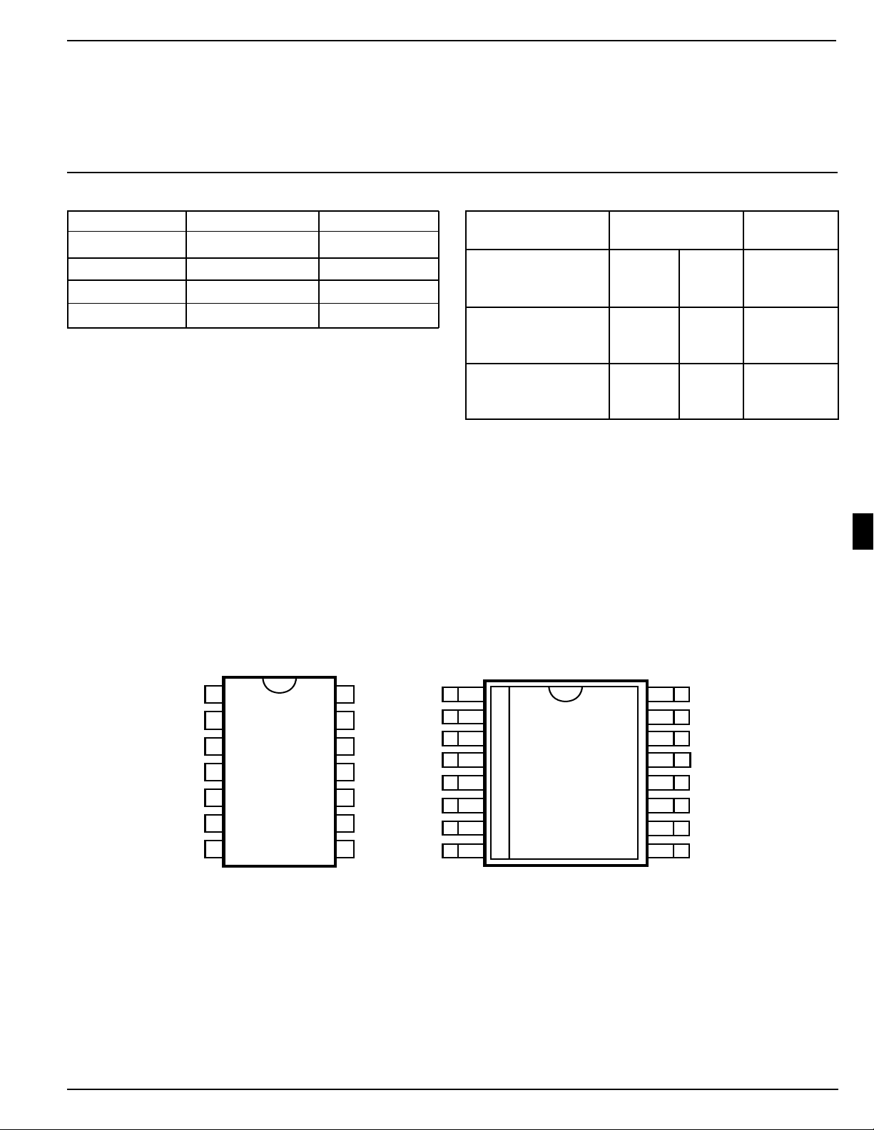
Pin Configurations
1A
1
1B
2
2A
3
2B
4
3A
5
3B
6
GND
7
14-Pin DIP (N)
TOP VIEW
14
13
12
11
10
5
16-Pin Wide SOIC (WM)
V
S
1Y
2Y
3Y
4Y
4B
9
4A
8
1A
1B
2A
2B
3A
3B
GND
GND
1
2
3
4
5
6
7
8
TOP VIEW
16
15
14
13
12
11
10
9
V
V
1Y
2Y
3Y
4Y
4B
4A
S
S
April 1998 5-81
Page 3
MIC4467/4468/4469 Micrel
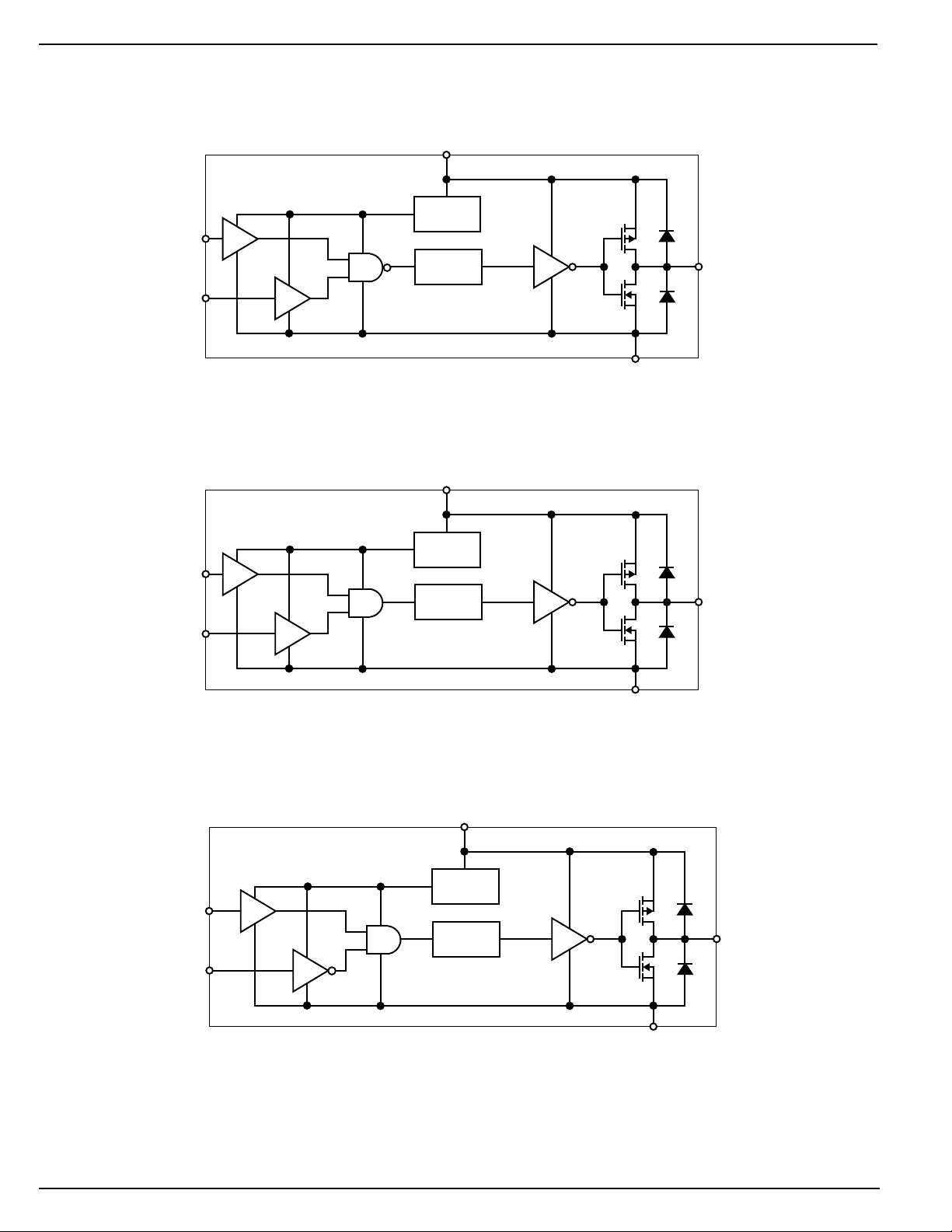
Block Diagrams
V
S
MIC4467
5V
Regulator
N A
Level
Shifter
N B
GND
Functional Diagram for One Driver (Four Drivers per Package–Ground Unused Inputs)
V
S
MIC4468
Y OUT
5V
Regulator
IN A
Level
Shifter
IN B
GND
unctional Diagram for One Driver (Four Drivers per Package–Ground Unused Inputs)
V
S
MIC4469
5V
Regulator
N A
Level
Shifter
N B
Y OUT
Y OUT
GND
Functional Diagram for One Driver (Four Drivers per Package–Ground Unused Inputs)
5-82 April 1998
Page 4

MIC4467/4468/4469 Micrel
Absolute Maximum Ratings (Notes 1 and 2)
Supply Voltage 22V
Input Voltage (GND – 5V) to (VS + 0.3V)
Maximum Chip Temperature
Power Dissipation
N Package (14-Pin Plastic DIP) 1.5W
WM Package (16-Pin Wide SOIC) 1W
Operating 150°C
Storage –65° to +150°C
Maximum Load Temperature
(10 sec, for soldering) 300°C
Package Thermal Resistance
N Package (14-Pin Plastic DIP) θ
WM Package (16-Pin Wide SOIC) θ
JA
JA
120°C/W
Operating Ambient Temperature
C Version 0° to +70°C
B Version –40° to +85°C
Electrical Characteristics: Measured at T
Symbol Parameter Conditions Min Typ Max Units
INPUT
V
IH
V
IL
I
IN
Logic 1 Input Voltage 2.4 1.3 V
Logic 0 Input Voltage 1.2 0.8 V
Input Current 0 ≤ VIN ≤ V
= 25°C with 4.5V ≤ VS ≤ 18V unless otherwise specified.
A
S
–1 1 µA
80°C/W
OUTPUT
V
OH
V
OL
R
O
I
PK
I Latch-Up Protection >500 mA
SWITCHING TIME
t
R
t
F
t
D1
t
D2
POWER SUPPLY
I
S
High Output Voltage I
Low Output Voltage I
Output Resistance I
Peak Output Current 1.2 A
Withstand Reverse Current
Rise Time Test Figure 1 14 25 ns
Fall Time Test Figure 1 13 25 ns
Delay Time Test Figure 1 30 75 ns
Delay Time Test Figure 1 45 75 ns
Power Supply Current 0.2 4 mA
Supply
= 10mA VS-0.15 V
LOAD
= 10mA 0.15 V
LOAD
= 10mA, VS = 18V 5 15 Ω
OUT
5
April 1998 5-83
Page 5

MIC4467/4468/4469 Micrel
Electrical Characteristics:
Measured over operating temperature range with 4.5V ≤ VS ≤ 18V unless otherwise specified.
Symbol Parameter Conditions Min Typ Max Units
INPUT
V
IH
V
IL
I
IN
Logic 1 Input Voltage 2.4 1.4 V
Logic 0 Input Voltage 1.0 0.8 V
Input Current 0 ≤ VIN ≤ V
S
–1 1 µA
OUTPUT
V
V
R
I
OH
OL
O
PK
High Output Voltage I
Low Output Voltage I
Output Resistance I
= 10 mA VS-0.3 V
LOAD
= 10 mA 0.3 V
LOAD
= 10 mA, VS = 18V 7 30 Ω
OUT
Peak Output Current 1.2 A
I Latch-Up Protection 500 mA
Withstand Reverse Current
SWITCHING TIME
t
R
t
F
t
D1
Rise Time Test Figure 1 17 50 ns
Fall Time Test Figure 1 16 50 ns
Delay Time Test Figure 1 35 100 ns
t
D2
Delay Time Test Figure 1 55 100 ns
POWER SUPPLY
I
S
Power Supply Current 0.4 8 mA
Supply
NOTE 1: Functional operation above the absolute maximum stress ratings is not implied.
NOTE 2: Static sensitive device. Store only in conductive containers. Handling personnel and equipment should be grounded to
prevent static damage.
5-84 April 1998
Page 6

MIC4467/4468/4469 Micrel
Typical Characteristics
Rise and Fall Time vs.
Supply Voltage
70
C = 1000pF
L
T = 25°C
60
A
50
40
30
Time (ns)
20
T
10
F
0
05 2010 15
SUPPLY VOLTAGE (V)
Delay Time vs. Temperature
35
C = 1000pF
L
V = 18V
30
S
25
20
15
Time (ns)
10
5
0
-50
-25 0 15025 50
-75
TEMPERATURE (°C)
T
R
75 100125
Delay Time vs. Supply Voltage
35
30
25
20
Time (ns)
15
10
T
D1
5
0
05 2010 15
SUPPLY VOLTAGE (V)
C = 1000pF
L
T = 25°C
A
T
D2
Supply Current vs.
Capacitive Load
80
T = 25°C
A
70
V = 18V
T
D2
S
60
50
T
D1
40
30
20
SUPPLY CURRENT (mA)
10
0
10 10000100
CAPACITIVE LOAD (pF)
1000
400kHz
20kHz
200
kHz
vs. Temperature
40
C = 1000pF
L
V = 18V
S
30
T
20
R
Time (ns)
10
-25 0 150
-50
-75
TEMPERATURE (°C)
Rise and Fall Time vs.
Capacitive Load
1k
T = 25°C
A
V = 18V
S
100
Time (ns)
10
1
10 10000100
CAPACITIVE LOAD (pF)
25 50
75
1000
T
100
F
125
T
R
T
F
5
Rise and Fall Time
Supply Current vs. Frequency
30
T = 25°C
A
C = 1000pF
L
20
10
SUPPLY CURRENT (mA)
0
1 100010
FREQUENCY (kHz)
5 V
100
V = 18V
S
10 V
High Output vs. Current
1.20
T = 25°C
A
.96
.72
S OUT
.48
| V – V | (V)
.24
.00
0 102030405060708090100
CURRENT SOURCED (mA)
V = 5V
C
15 V
10 V
Low Output vs. Current
1.20
T = 25°C
A
.96
.72
.48
.24
OUTPUT VOLTAGE (V)
.00
010
20 30 40 50 60 70 80 90 100
CURRENT SUNK (mA)
V = 5V
S
15 V
10 V
April 1998 5-85
Page 7

MIC4467/4468/4469 Micrel
Test Figure 1
1 µF FILM
IN
1
IN
1
IN
2
IN
2
IN
3
IN
3
IN
4
IN
4
Quiescent Power Supply
Current vs. Supply Voltage
2.5
2.0
1.5
1.0
0.5
SUPPLY CURRENT (mA)
0
V
S
NO LOAD
BOTH INPUTS LOGIC "1"
T = 25°C
A
10
SUPPLY VOLTAGE (V)
0.1 µF CERAMIC
V
OUT
470 pF
Quiescent Power Supply
Current vs. Supply Voltage
400
300
200
150
NO LOAD
100
SUPPLY CURRENT (µA)
50
201550
0
BOTH INPUTS LOGIC "0"
T = 25°C
A
SUPPLY VOLTAGE (V)
INVERTING INPUT
+5V
V
INPUT
10%
t
V
OUTPUT
18V
0V
D1
90%
t
F
NON-INVERTING INPUT
+5V
V
INPUT
10%
18V
V
OUTPUT
0V
90%
t
D1
10%
10%
151005
10%
t
R
90%
t
D2
90%
90%
t
D2
20
t
R
10%
90%
t
F
Package Power Dissipation
1500
1250
1000
750
D
P (mW)
500
16-PIN WIDE SOIC
250
SLOPE = –8 mW/°C
0
25 50 75 100 125 150
AMBIENT TEMPERATURE (°C)
14-PIN PDIP
SLOPE = –12 mW/°C
Quad Driver Drives H Bridge to
Control Motor Speed and Direction
+5V TO +15V
MIC4467
CW
CCW
DC BRUSH
MOTOR
PWM SPEED
GND
5-86 April 1998
 Loading...