

Page 1
MIC4416/4417 Micrel, Inc.
MIC4416/4417
IttyBitty™ Low-Side MOSFET Driver
General Description
The MIC4416 and MIC4417 IttyBitty™ low-side MOSFET
drivers are designed to switch an N-channel enhancementtype MOSFET from a TTL-compatible control signal in lowside switch applications. The MIC4416 is noninverting and
the MIC4417 is inverting. These drivers feature short delays
and high peak current to produce precise edges and rapid
rise and fall times. Their tiny 4-lead SOT-143 package uses
minimum space.
The MIC4416/7 is powered from a +4.5V to +18V supply
voltage. The on-state gate drive output voltage is approximately equal to the supply voltage (no internal regulators or
clamps). High supply voltages, such as 10V, are appropriate
for use with standard N-channel MOSFETs. Low supply
voltages, such as 5V, are appropriate for use with logic-level
N-channel MOSFETs.
In a low-side configuration, the driver can control a MOSFET
that switches any voltage up to the rating of the MOSFET.
The MIC4416 is available in the SOT-143 package and
is rated for –40°C to +85°C ambient temperature range.
Features
• +4.5V to +18V operation
• Low steady-state supply current
50µA typical, control input low
370µA typical, control input high
•1.2A nominal peak output
3.5Ω typical output resistance at 18V supply
7.8Ω typical output resistance at 5V supply
• 25mV maximum output offset from supply or ground
• Operates in low-side switch circuits
• TTL-compatible input withstands –20V
• ESD protection
•Inverting and noninverting versions
Applications
• Battery conservation
• Solenoid and motion control
• Lamp control
• Switch-mode power supplies
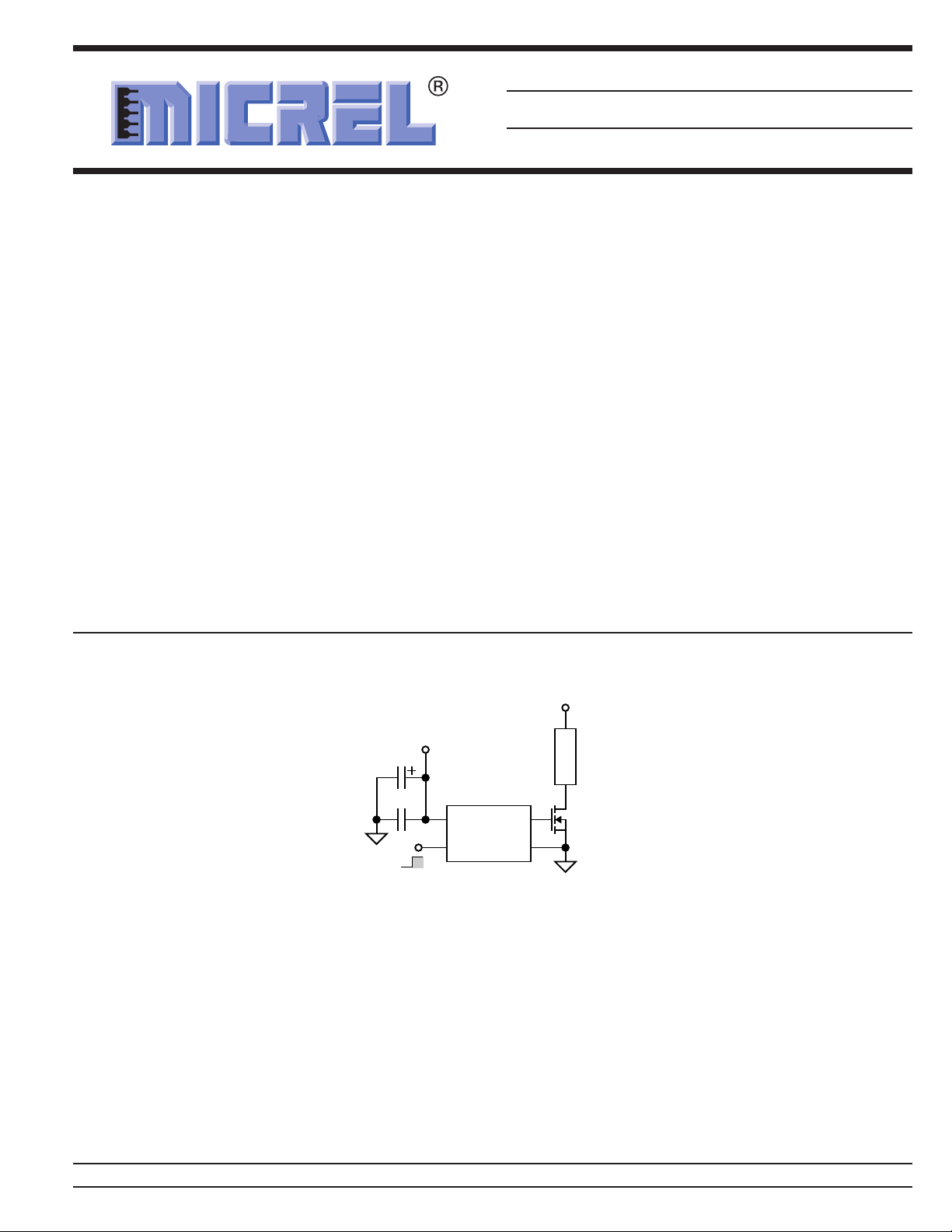
Typical Application
*Siliconix
30mΩ, 7A max.
†
Load voltage limited only by
MOSFET drain-to-source rating
+12V
4.7µF
0.1µF
On
Off
MIC4416
32
VS
4
CTLGGND
Low-Side Power Switch
Load
Voltage
1
†
Load
Si9410DY*
N-channel
MOSFET
Micrel, Inc. • 2180 Fortune Drive • San Jose, CA 95131 • USA • tel + 1 (408) 944-0800 • fax + 1 (408) 474-1000 • http://www.micrel.com
May 2005 1 MIC4416/4417
Page 2
MIC4416/4417 Micrel, Inc.
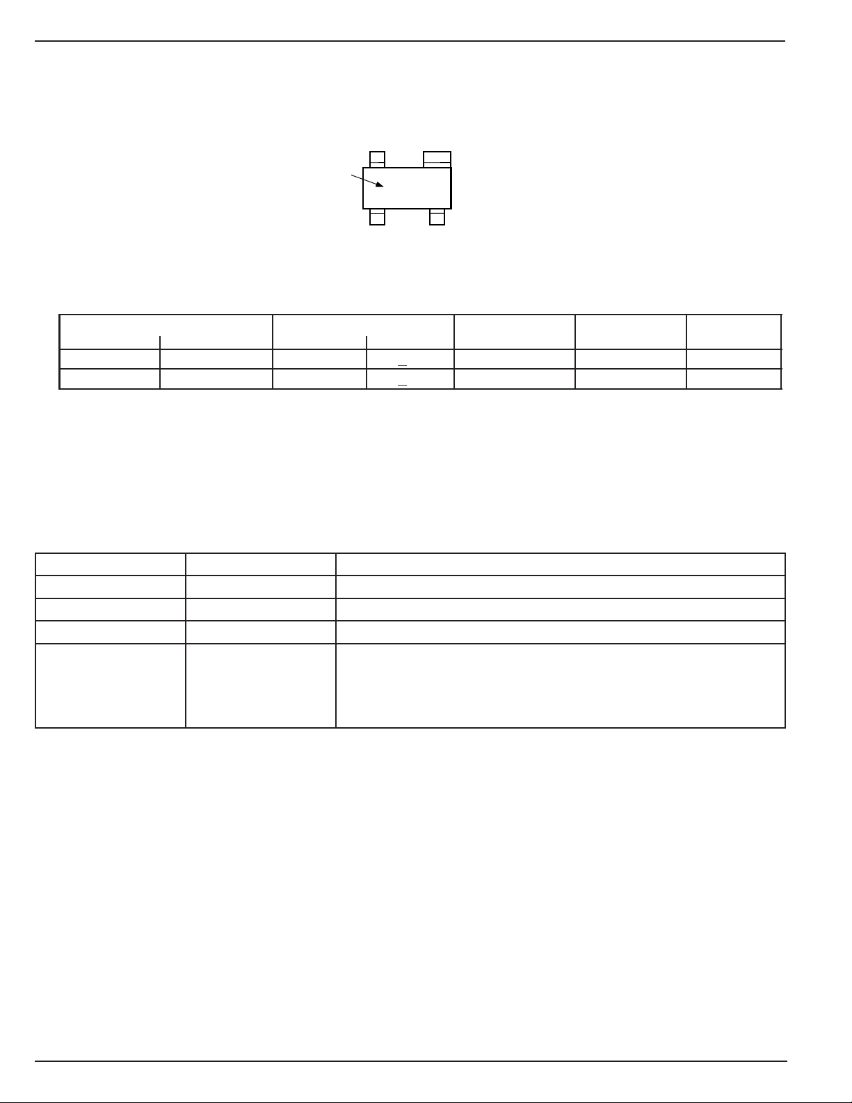
Pin Configuration
G
Part
Identification
34
GND
12
Dxx
CTLVS
SOT-143 (M4)
Part Number Marking Code* Temperature
Standard Pb-Free Standard Pb-Free Range Configuration Package
MIC4416BM4 MIC4416YM4 D10 D10 –40ºC to +85ºC Non-Inverting SOT-143
MIC4417BM4 MIC4417YM4 D11 D11 –40ºC to +85ºC Inverting SOT-143
*Under bar symbol (_) may not be to scale.
Pin Description
Pin Number Pin Name Pin Function
1 GND Ground: Power return.
2GGate (Output) : Gate connection to external MOSFET.
3VSSupply (Input): +4.5V to +18V supply.
4 CTL Control (Input): TTL-compatible on/off control input.
MIC4416 only: Logic high forces the gate output to the supply voltage.
Logic low forces the gate output to ground.
MIC4417 only: Logic high forces the gate output to ground. Logic low
forces the gate output to the supply voltage.
MIC4416/4417 2 May 2005
Page 3
MIC4416/4417 Micrel, Inc.
Absolute Maximum Ratings
Supply Voltage (VS) .................................................... +20V
Control Voltage (V
Gate Voltage (VG) .......................................................+20V
Junction Temperature (TJ) ........................................ 150°C
Lead Temperature, Soldering ................... 260°C for 5 sec.
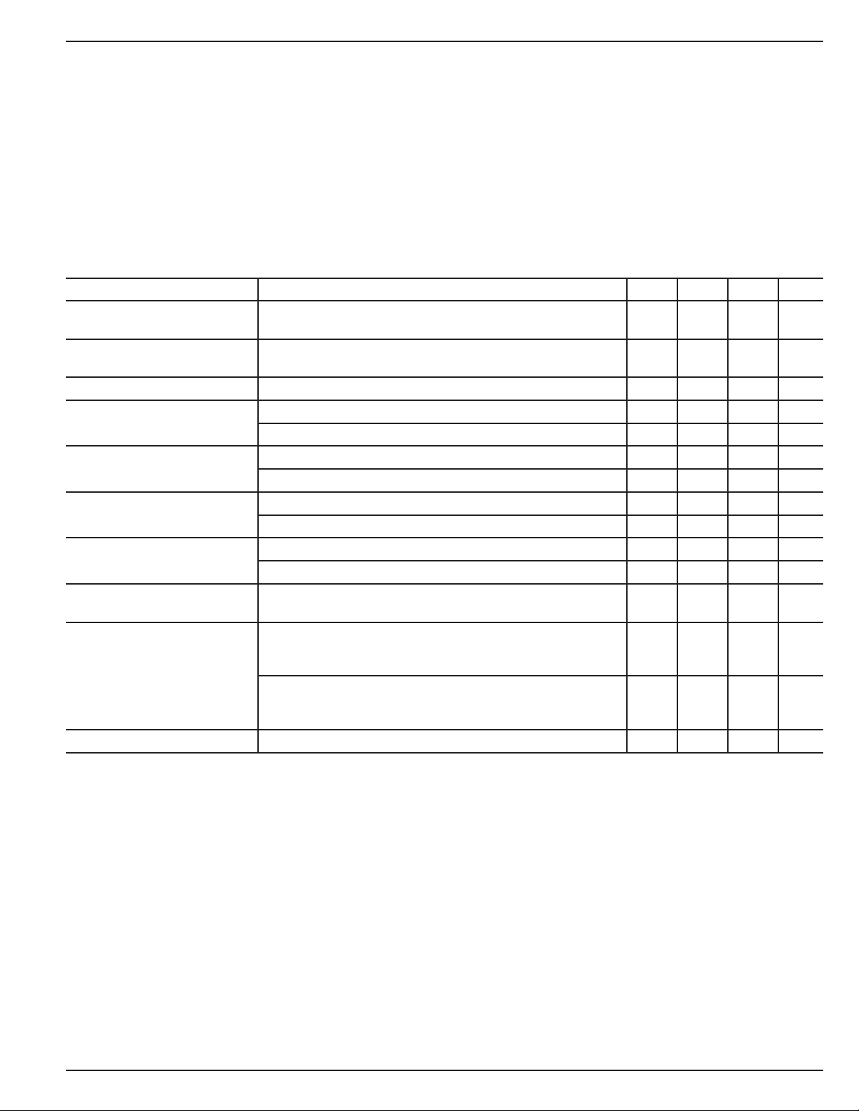
Electrical Characteristics
) .................................. –20V to +20V
CTL
(Note 3)
Operating Ratings
Supply Voltage (VS) ....................................... +4.5 to +18V
Control Voltage (V
Ambient Temperature Range (TA) ............. –40°C to +85°C
Thermal Resistance (θJA)......................................220°C/W
(soldered to 0.25in2 copper ground plane)
) .......................................... 0V to V
CTL
Parameter Condition (Note 1) Min Typ Max Units
Supply Current 4.5V ≤ V
Control Input Voltage 4.5V ≤ V
Control Input Current 0V ≤ V
Delay Time, V
Rising VS = 5V CL = 1000pF, Note 2 42 ns
CTL
≤ 18V V
S
≤ 18V V
S
≤ V
CTL
S
= 0V 50 200 µA
CTL
V
= 5V 370 1500 µA
CTL
for logic 0 input 0.8 V
CTL
V
for logic 1 input 2.4 V
CTL
–10 10 µA
VS = 18V CL = 1000pF, Note 2 33 60 ns
Delay Time, V
Falling VS = 5V CL = 1000pF, Note 2 42 ns
CTL
VS = 18V CL = 1000pF, Note 2 23 40 ns
Output Rise Time VS = 5V CL = 1000pF, Note 2 24 ns
VS = 18V CL = 1000pF, Note 2 14 40 ns
Output Fall Time VS = 5V CL = 1000pF, Note 2 28 ns
VS = 18V CL = 1000pF, Note 2 16 40 ns
Gate Output Offset Voltage 4.5V ≤ VS ≤ 18V VG = high –25 mV
VG = low 25 mV
Output Resistance V
= 5V, I
S
OUT
= 10mA
P-channel (source) MOSFET 7.6 Ω
N-channel (sink) MOSFET 7.8 Ω
VS = 18V, I
OUT
= 10mA
P-channel (source) MOSFET 3.5 10 Ω
N-channel (sink) MOSFET 3.5 10 Ω
Gate Output Reverse Current No latch up 250 mA
S
General Note: Devices are ESD protected, however handling precautions are recommended.
Note 1: Typical values at TA = 25°C. Minimum and maximum values indicate performance at –40°C ≥ TA ≥ +85°C. Parts production tested at 25°C.
Note 2: Refer to “MIC4416 Timing Definitions” and “MIC4417 Timing Definitions” diagrams (see next page).
Note 3: Specification for packaged product only.
May 2005 3 MIC4416/4417
Page 4
MIC4416/4417 Micrel, Inc.
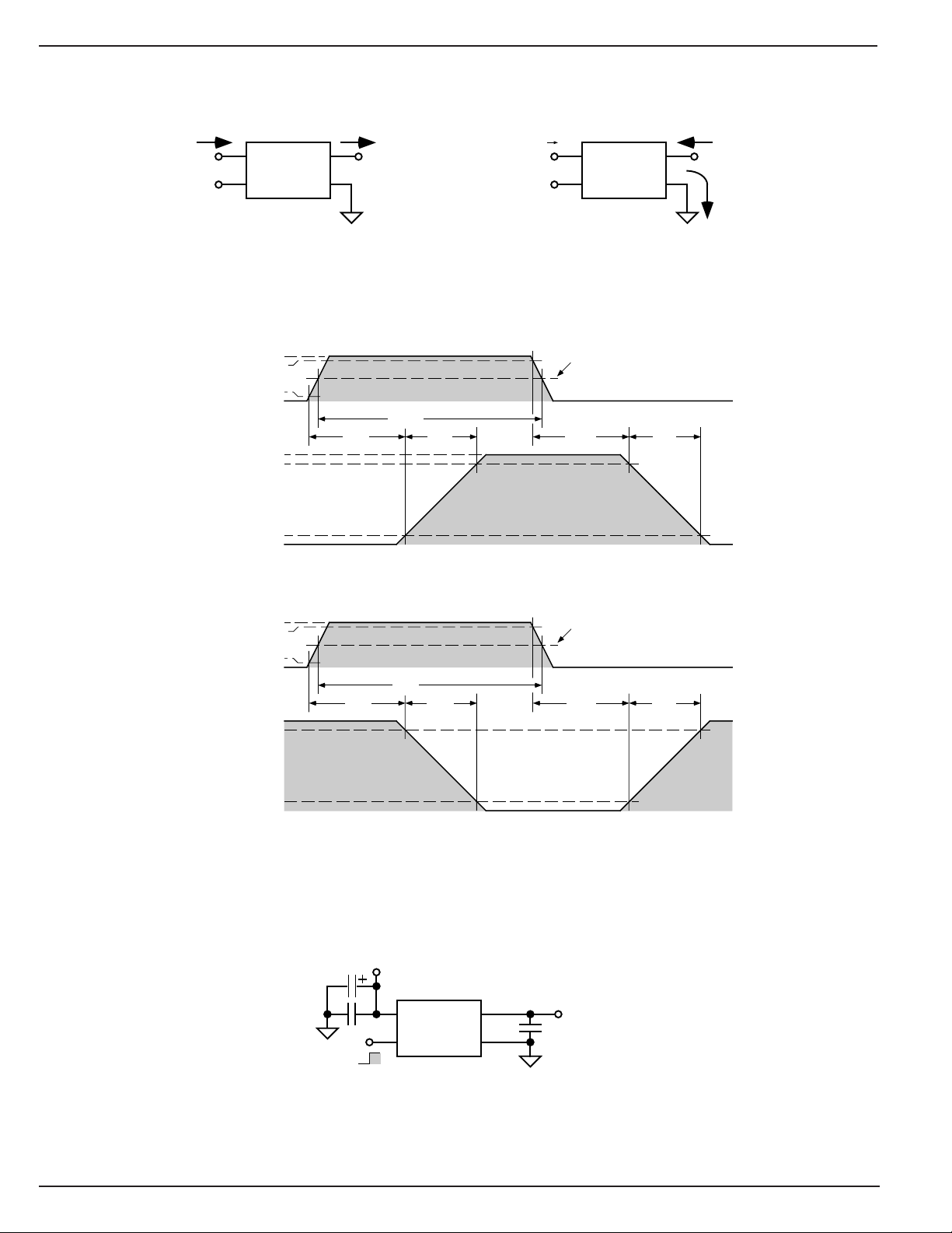
Definitions
I
V
SUPPLY
MIC4416 = high
MIC4417 = low
(P-channel on, N-channel off)
INPUT
OUTPUT
SUPPLY
MIC4416/7
32
VS
4
CTLGGND
1
Source State
MIC4416/MIC4417 Operating States
5V
90%
10%
0V
V
S
90%
10%
0V
I
OUT
delay
time
I
I
SUPPLY
V
V
≈ V
OUT
SUPPLY
SUPPLY
MIC4416 = low
MIC4417 = high
MIC4416/7
32
VS
4
CTLGGND
OUT
V
≈ GND
OUT
1
Sink State
(P-channel off, N-channel on)
2.5V
pulse
width
rise
time
delay
time
fall
time
Test Circuit
INPUT
OUTPUT
5V
90%
10%
0V
V
90%
10%
0V
MIC4416 (Noninverting) Timing Definitions
pulse
time
width
rise
time
delay
S
MIC4417 (Inverting) Timing Definitions
V
SUPPLY
MIC4416/7
32
VS
4
5V
0V
CTLGGND
1
2.5V
delay
time
V
OUT
C
L
fall
time
MIC4416/4417 4 May 2005
Page 5
MIC4416/4417 Micrel, Inc.
0
10
20
30
40
50
-60 -30 0 30 60 90 120 150
TIME (ns)
TEMPERATURE (°C)
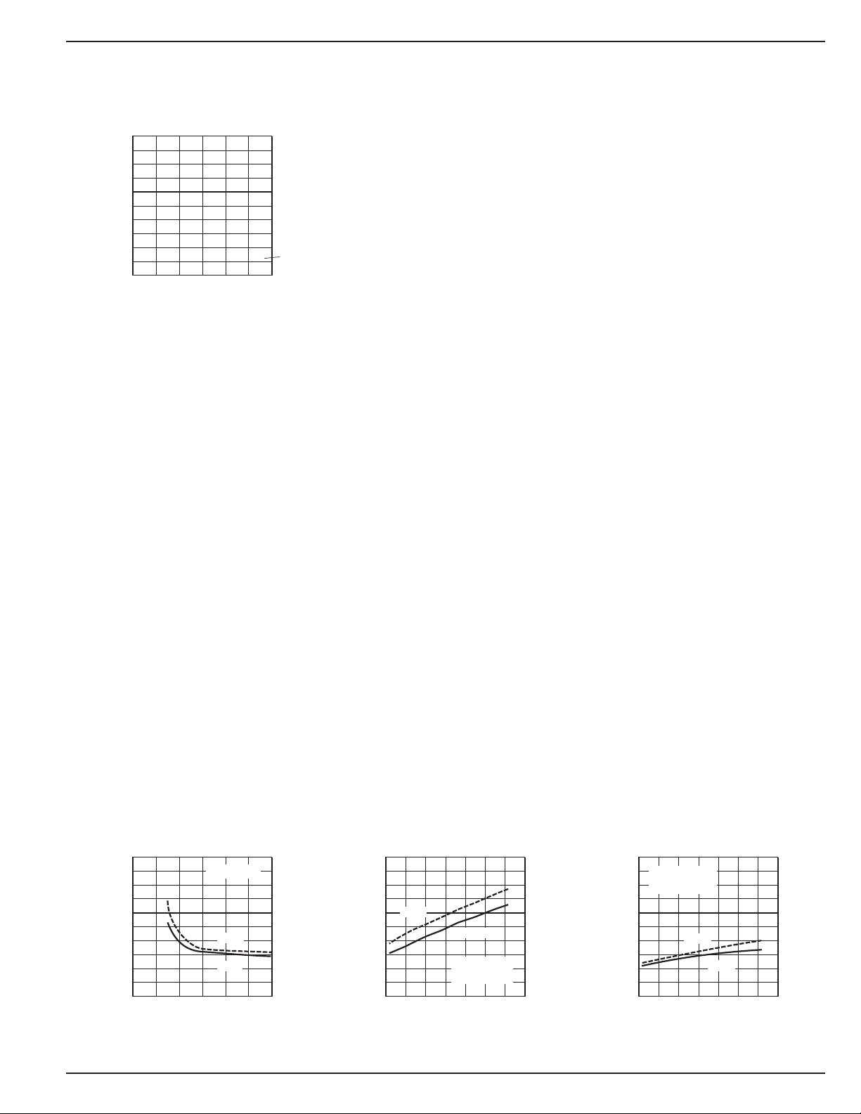
Typical Characteristics Note 3
Rise and Fall Time
vs. Supply Voltage
50
40
30
20
May 2005 5 MIC4416/4417
TIME (ns)
10
0
0369121518
SUPPLY VOLTAGE (V)
f
CTL
= 1MHz
FALL
RISE
Rise and Fall Time
vs. Temperature
50
40
FALL
30
V
SUPPLY
f
CTL
RISE
= 5V
= 1MHz
20
TIME (ns)
10
0
-60 -30 0 30 60 90 120 150
TEMPERATURE (°C)
Rise and Fall Time
vs. Temperature
V
= 18V
SUPPLY
f
= 1MHz
CTL
FALL
RISE
Page 6
MIC4416/4417 Micrel, Inc.
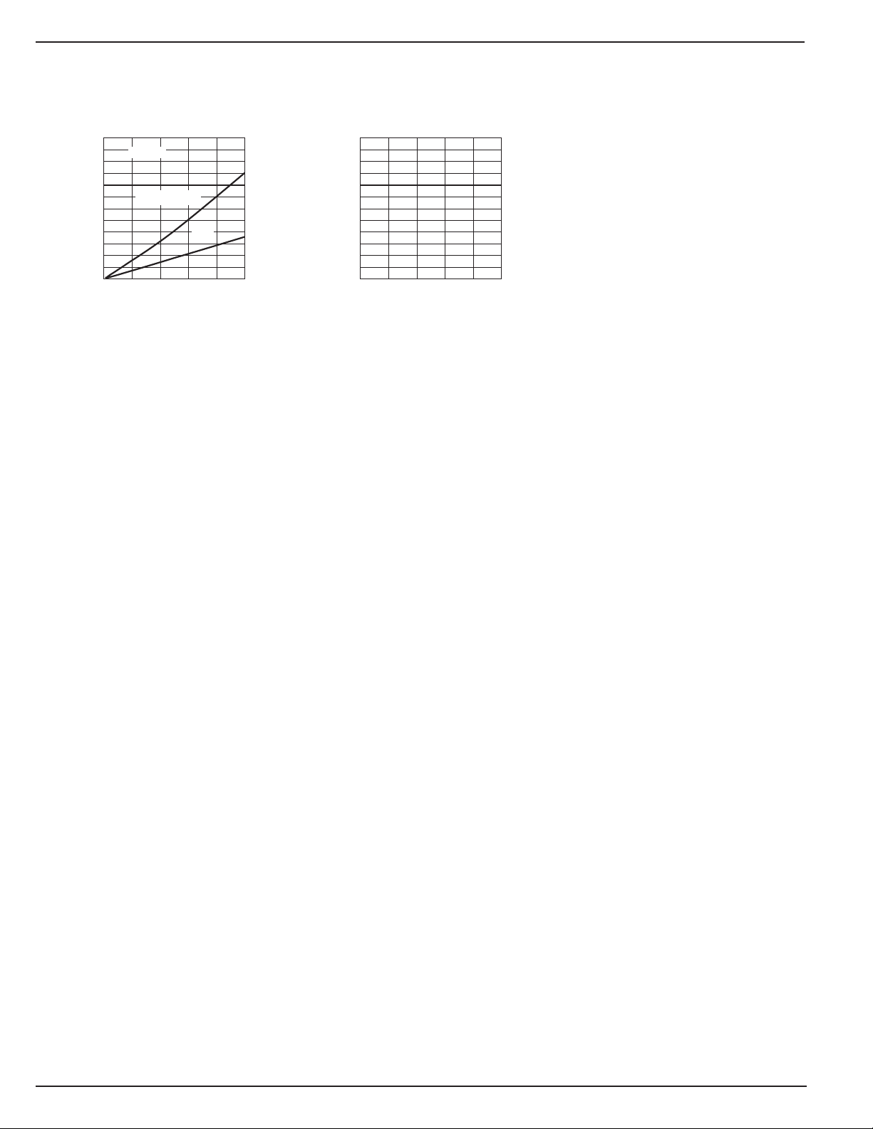
Output Voltage Drop vs.
Output Source Current
1200
1000
800
600
400
VOLTAGE DROP (mV)
200
NOTE 4
V
= 5V
SUPPLY
18V
0
020406080100
OUTPUT CURRENT (mA)
MIC4416/4417 6 May 2005
Page 7
MIC4416/4417 Micrel, Inc.
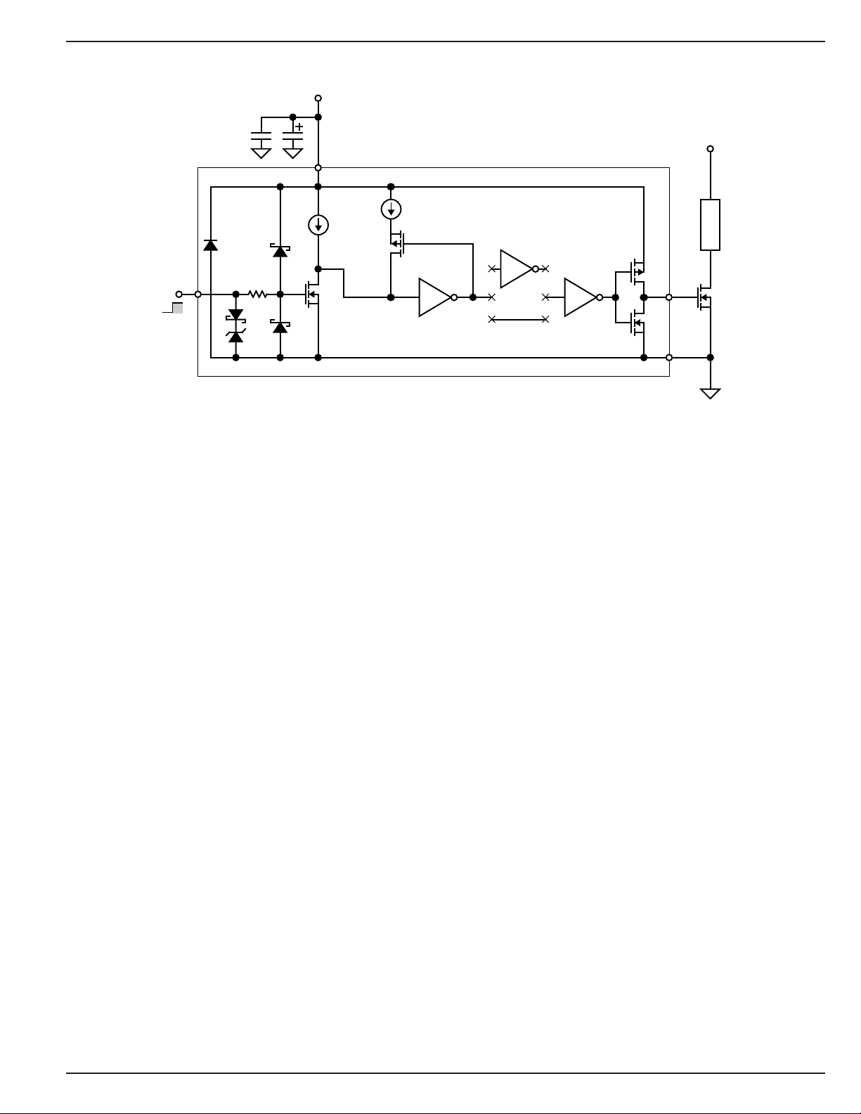
Functional Diagram
V
SUPPLY
V
SWITCHED
VS
0.6mA
MIC4417
INVERTING
MIC4416
NONINVERTING
Load
Q3
G
Q4
GND
CTL
Logic-Level
Input
D1
0.3mA
Q2
R1
2k
D2
D3
35V
D4
Q1
D5
Functional Diagram with External Components
Functional Description
Refer to the functional diagram.
The MIC4416 is a noninverting driver. A logic high on the CTL
(control) input produces gate drive output. The MIC4417 is
an inverting driver. A logic low on the CTL (control) input
produces gate drive output. The G (gate) output is used to
turn on an external N-channel MOSFET.
Supply
VS (supply) is rated for +4.5V to +18V. External capacitors
are recommended to decouple noise.
Control
CTL (control) is a TTL-compatible input. CTL must be forced
high or low by an external signal. A floating input will cause
unpredictable operation.
A high input turns on Q1, which sinks the output of the 0.3mA
and the 0.6mA current source, forcing the input of the first
inverter low.
Hysteresis
The control threshold voltage, when CTL is rising, is slightly
higher than the control threshold voltage when CTL is falling.
When CTL is low, Q2 is on, which applies the additional
0.6mA current source to Q1. Forcing CTL high turns on Q1
which must sink 0.9mA from the two current sources. The
higher current through Q1 causes a larger drain-to-source
voltage drop across Q1. A slightly higher control voltage is
required to pull the input of the first inverter down to its
threshold.
Q2 turns off after the first inverter output goes high. This
reduces the current through Q1 to 0.3mA. The lower current
reduces the drain-to-source voltage drop across Q1. A
slightly lower control voltage will pull the input of the first
inverter up to its threshold.
Drivers
The second (optional) inverter permits the driver to be manufactured in inverting and noninverting versions.
The last inverter functions as a driver for the output MOSFETs
Q3 and Q4.
Gate Output
G (gate) is designed to drive a capacitive load. VG (gate
output voltage) is either approximately the supply voltage or
approximately ground, depending on the logic state applied
to CTL.
If CTL is high, and VS (supply) drops to zero, the gate output
will be floating (unpredictable).
ESD Protection
D1 protects VS from negative ESD voltages. D2 and D3
clamp positive and negative ESD voltages applied to CTL.
R1 isolates the gate of Q1 from sudden changes on the CTL
input. D4 and D5 prevent Q1’s gate voltage from exceeding
the supply voltage or going below ground.
May 2005 7 MIC4416/4417
Page 8
MIC4416/4417 Micrel, Inc.
VS
CTLGGND
MIC4416
4.7µF
+8V to +18V
1
32
4
Load
Logic
Input
*Gate enhancement voltage
VGS*
+15V
Standard
MOSFET
IRFZ24
†
†
International Rectifier
100m
Ω
, 60V MOSFET
0.1µF
Try a
15
Ω
, 15W
or
1k, 1/4W
resistor
VS
CTLGGND
MIC4416
+4.5V to 10V*
1
32
4
Load
Logic
Input
*Gate enhancement voltage
(must not exceed 10V)
VGS*
+5V
Logic-Level
MOSFET
IRLZ44
†
†
International Rectifier
28m
Ω
, 60V MOSFET
4.7µF
0.1µF
Try a
3
Ω
, 10W
or
100
Ω
, 1/4W
resistor
Application Information
The MIC4416/7 is designed to provide high peak current for
charging and discharging capacitive loads. The 1.2A peak
value is a nominal value determined under specific conditions. This nominal value is used to compare its relative size
to other low-side MOSFET drivers. The MIC4416/7 is not
designed to directly switch 1.2A continuous loads.
Supply Bypass
Capacitors from VS to GND are recommended to control
switching and supply transients. Load current and supply
lead length are some of the factors that affect capacitor
size requirements.
A 4.7µF or 10µF tantalum capacitor is suitable for many
applications. Low-ESR (equivalent series resistance) metalized film capacitors may also be suitable. An additional 0.1µF
ceramic capacitor is suggested in parallel with the larger
capacitor to control high-frequency transients.
The low ESR (equivalent series resistance) of tantalum
capacitors makes them especially effective, but also makes
Logic-Level MOSFET
Logic-level N-channel power MOSFETs are fully enhanced
with a gate-to-source voltage of approximately 5V and have
an absolute maximum gate-to-source voltage of ±10V. They
are less common and generally more expensive.
The MIC4416/7 can drive a logic-level MOSFET if the supply
voltage, including transients, does not exceed the maximum
MOSFET gate-to-source rating (10V).
them susceptible to uncontrolled inrush current from low
impedance voltage sources (such as NiCd batteries or automatic test equipment). Avoid instantaneously applying voltage, capable of very high peak current, directly to or near
tantalum capacitors without additional current limiting. Normal power supply turn-on (slow rise time) or printed circuit
trace resistance is usually adequate for normal product
usage.
Circuit Layout
Avoid long power supply and ground traces. They exhibit
inductance that can cause voltage transients (inductive kick).
Even with resistive loads, inductive transients can sometimes
exceed the ratings of the MOSFET and the driver.
When a load is switched off, supply lead inductance forces
current to continue flowing—resulting in a positive voltage
spike. Inductance in the ground (return) lead to the supply
has similar effects, except the voltage spike is negative.
At low voltages, the MIC4416/7’s internal P- and N-channel
MOSFET’s on-resistance will increase and slow the output
rise time. Refer to “Typical Characteristics” graphs.
Inductive Loads
Switching transitions momentarily draw current from VS to
GND. This combines with supply lead inductance to create
voltage transients at turn on and turnoff.
Transients can also result in slower apparent rise or fall times
when driver’s ground shifts with respect to the control input.
Minimize the length of supply and ground traces or use
ground and power planes when possible. Bypass capacitors
should be placed as close as practical to the driver.
MOSFET Selection
Standard MOSFET
A standard N-channel power MOSFET is fully enhanced with
a gate-to-source voltage of approximately 10V and has an
absolute maximum gate-to-source voltage of ±20V.
The MIC4416/7’s on-state output is approximately equal to
the supply voltage. The lowest usable voltage depends upon
the behavior of the MOSFET.
MIC4416/4417 8 May 2005
Switching off an inductive load in a low-side application forces
the MOSFET drain higher than the supply voltage (as the
inductor resists changes to current). To prevent exceeding
the MOSFET’s drain-to-gate and drain-to-source ratings, a
Schottky diode should be connected across the inductive
load.
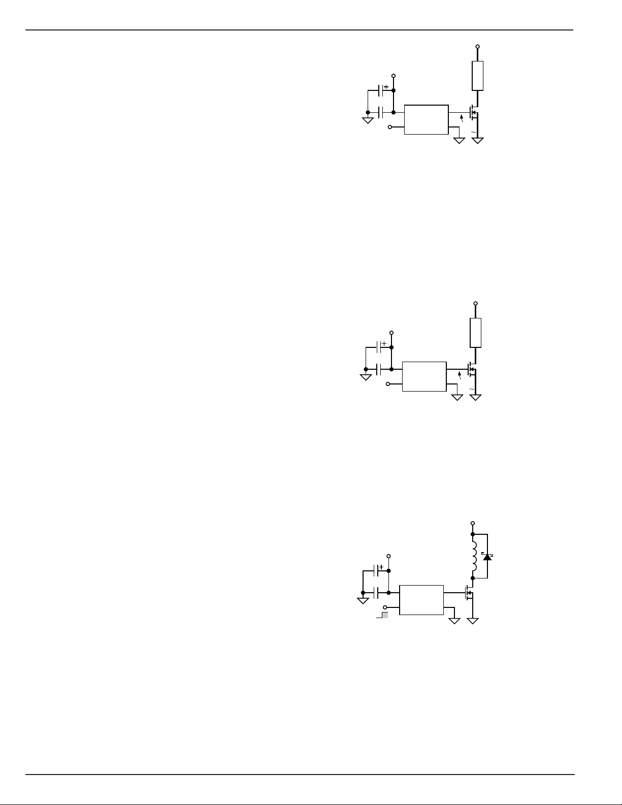
Figure 1. Using a Standard MOSFET
Figure 2. Using a Logic-Level MOSFET
V
SWITCHED
V
4.7µF
0.1µF
On
Off
SUPPLY
MIC4416
32
VS
4
CTLGGND
1
Schottky
Diode
Figure 3. Switching an Inductive Load
Page 9
MIC4416/4417 Micrel, Inc.
VS
CTLGGND
MIC4416
+4.5V to 18V
1
32
4
Logic
Input
+5V
Logic-Level
MOSFET
IRL3103*
* International Rectifier
14m
Ω
, 30V MOSFET,
logic-level, V
GS
= ±20V max.
4.7µF
0.1µF
Compare
47k
Ω
, 5W
to
1k
Ω
, 1/4W
loads
G
D
S
Slower rise time
observed at
MOSFET’s drain
Power Dissipation
The maximum power dissipation must not be exceeded to
prevent die meltdown or deterioration.
Power dissipation in on/off switch applications is negligible.
Fast repetitive switching applications, such as SMPS (switchmode power supplies), cause a significant increase in power
dissipation with frequency. Power is dissipated each time
current passes through the internal output MOSFETs when
charging or discharging the external MOSFET. Power is also
dissipated during each transition when some current momentarily passes from VS to GND through both internal MOSFETs.
Power dissipation is the product of supply voltage and supply
current:
1) PD = VS × I
S
where:
PD = power dissipation (W)
VS = supply voltage (V)
IS = supply current (A) [see paragraph below]
Supply current is a function of supply voltage, switching
frequency, and load capacitance. Determine this value from
the “Typical Characteristics: Supply Current vs. Frequency”
graph or measure it in the actual application.
Do not allow PD to exceed P
D (max)
, below.
TJ (junction temperature) is the sum of TA (ambient temperature) and the temperature rise across the thermal resistance
of the package. In another form:
150 T
−
2)
P
≤
D
A
220
where:
P
= maximum power dissipation (W)
D (max)
150 = absolute maximum junction temperature (°C)
TA = ambient temperature (°C) [68°F = 20°C]
220 = package thermal resistance (°C/W)
Maximum power dissipation at 20°C with the driver soldered
to a 0.25in2 ground plane is approximately 600mW.
G
PCB heat sink/
ground plane
GND
High-Frequency Operation
Although the MIC4416/7 driver will operate at frequencies
greater than 1MHz, the MOSFET’s capacitance and the load
will affect the output waveform (at the MOSFET’s drain).
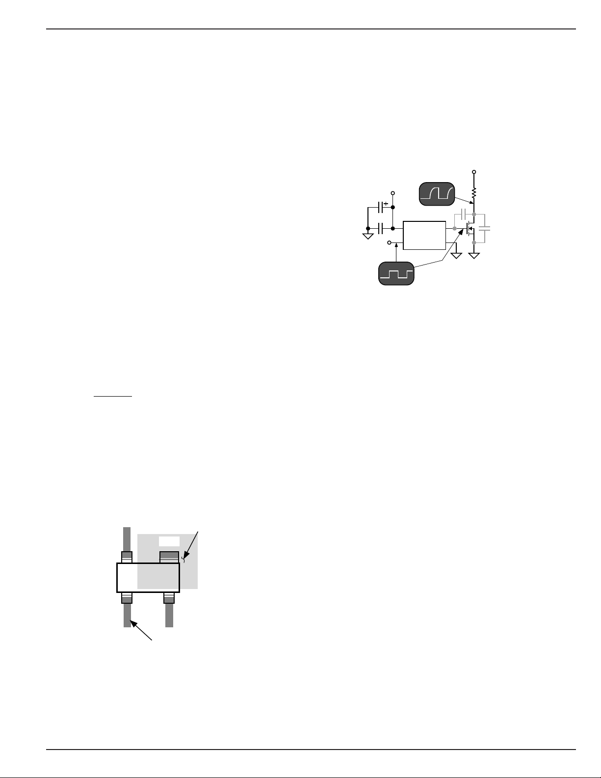
For example, an MIC4416/IRL3103 test circuit using a 47Ω
5W load resistor will produce an output waveform that closely
matches the input signal shape up to about 500kHz. The
same test circuit with a 1kΩ load resistor operates only up to
about 25kHz before the MOSFET source waveform shows
significant change.
Figure 5. MOSFET Capacitance Effects at High
Switching Frequency
When the MOSFET is driven off, the slower rise occurs
because the MOSFET’s output capacitance recharges through
the load resistance (RC circuit). A lower load resistance
allows the output to rise faster. For the fastest driver operation, choose the smallest power MOSFET that will safely
handle the desired voltage, current, and safety margin. The
smallest MOSFETs generally have the lowest capacitance.
VS
The SOT-143 package θJA (junction-to-ambient thermal resistance) can be improved by using a heat sink larger than the
specified 0.25in2 ground plane. Significant heat transfer
occurs through the large (GND) lead. This lead is an
extension of the paddle to which the die is attached.
May 2005 9 MIC4416/4417
Figure 4. Heat-Sink Plane
CTL
PCB traces
Page 10
MIC4416/4417 Micrel, Inc.
Package Information
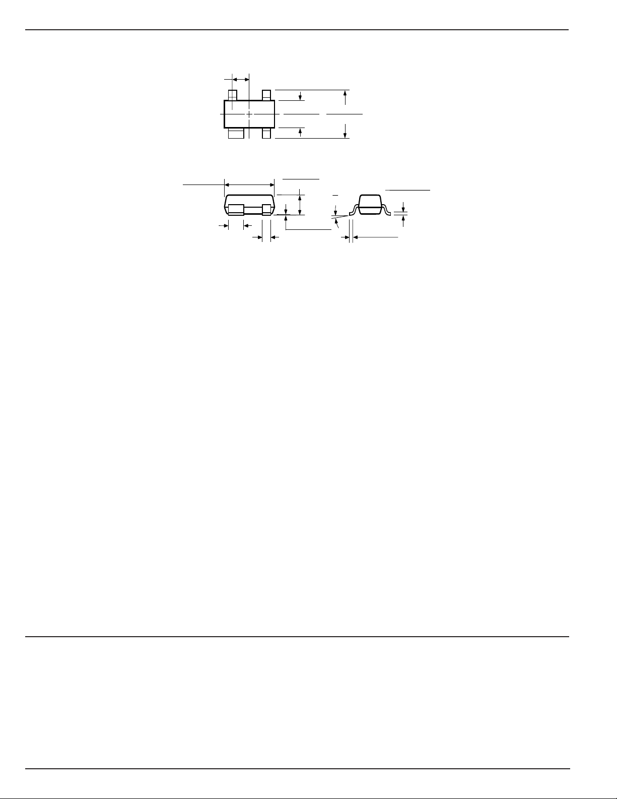
0.950 (0.0374) TYP
C
L
C
L
3.05 (0.120)
2.67 (0.105)
0.800 (0.031) TYP
0.400 (0.016) TYP 3 PLACES
4-Pin SOT-143 (M4)
1.40 (0.055)
1.20 (0.047)
1.12 (0.044)
0.81 (0.032)
0.10 (0.004)
0.013 (0.0005)
2.50 (0.098)
2.10 (0.083)
DIMENSIONS:
MM (INCH)
8°
0°
0.41 (0.016)
0.13 (0.005)
0.150 (0.0059)
0.089 (0.0035)
MICREL INC. 2180 FORTUNE DRIVE SAN JOSE, CA 95131 USA
TEL + 1 (408) 944-0800 FAX + 1 (408) 474-1000 WEB http://www.micrel.com
This information furnished by Micrel in this data sheet is believed to be accurate and reliable. However no responsibility is assumed by Micrel for its use.
Micrel Products are not designed or authorized for use as components in life support appliances, devices or systems where malfunction of a product can
reasonably be expected to result in personal injury. Life support devices or systems are devices or systems that (a) are intended for surgical implant into
the body or (b) support or sustain life, and whose failure to perform can be reasonably expected to result in a significant injury to the user. A Purchaser’s
use or sale of Micrel Products for use in life support appliances, devices or systems is a Purchaser’s own risk and Purchaser agrees to fully indemnify
Micrel reserves the right to change circuitry and specifications at any time without notification to the customer.
Micrel for any damages resulting from such use or sale.
© 2001 Micrel Incorporated
MIC4416/4417 10 May 2005
 Loading...