

Page 1
MIC4043 Micrel
MIC4043
Low-Voltage Secondary-Side Shunt Regulator
General Description
The MIC4043 is a shunt regulator optimized for secondaryside regulation in low-voltage power supplies. Featuring an
output stage guaranteed to swing within 400mV of ground,
the MIC4043 can be used in power supplies operating down
to 1.8V, even with optoisolators requiring greater than 1.2V of
headroom.
In power supply applications, the MIC4043 normally drives
the LED of an optically isolated feedback circuit. The MIC4043
monitors a resistively-divided output voltage and sinks error
current through the optoisolator’s LED (secondary side); the
optoisolator’s transistor (primary side) provides this signal to
the controller’s feedback input. The MIC4043 is also practical
for other voltage-monitoring applications requiring an opencollector output.
The MIC4043 replaces conventional ’431-type shunt regulators to allow low-voltage applications where there is inadequate headroom for a 2.5V regulator in series with an
optoisolator. Replacing ’431-type devices requires only a
minor change to the way that the resistive-divider values are
calculated.
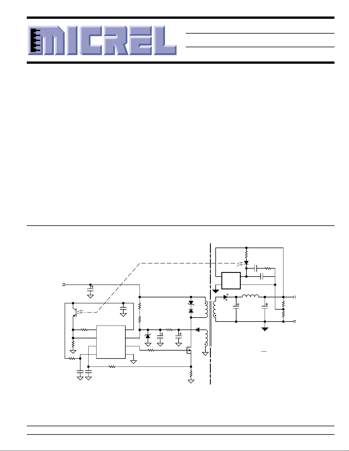
Typical Application
Features
• Ideal for 1.8V switching converters
• Low-voltage operation
400mV maximum saturation over
operating temperature range
• Easy to use
voltage in, current out
• 2% voltage tolerance over operating temperature range
Applications
• Optically isolated low-volage power supplies
• Low-voltage discrete regulator control
OPTICAL
ISOLATION
MIC4043
V
IN
MIC38HC43BN
1
2
3
4
COMP
FB
I
SNS
RT/C
T
V
REF
V
V
OUT
GND
8
7
DD
6
5
Low-Side Feedback
Control
1
2
4
3
7
6
PRIMARY SIDE
SECONDARY SIDE
MIC4043
SNKIN
FBGND
V 1.245V
OUT
COMPENSATION
R1
R2
R2
=+
1
R1
V
OUT
Return
200kHz DC-DC Flyback Converter
Micrel, Inc. • 1849 Fortune Drive • San Jose, CA 95131 • USA • tel + 1 (408) 944-0800 • fax + 1 (408) 944-0970 • http://www.micrel.com
May 2000 1 MIC4043
Page 2
MIC4043 Micrel
Ordering Information
Part Number Marking Voltage Tolerance Configuration Temperature Range Package
MIC4043BM4 RBAD 1.245V 1% Open Collector –40°C to +85°C SOT-143
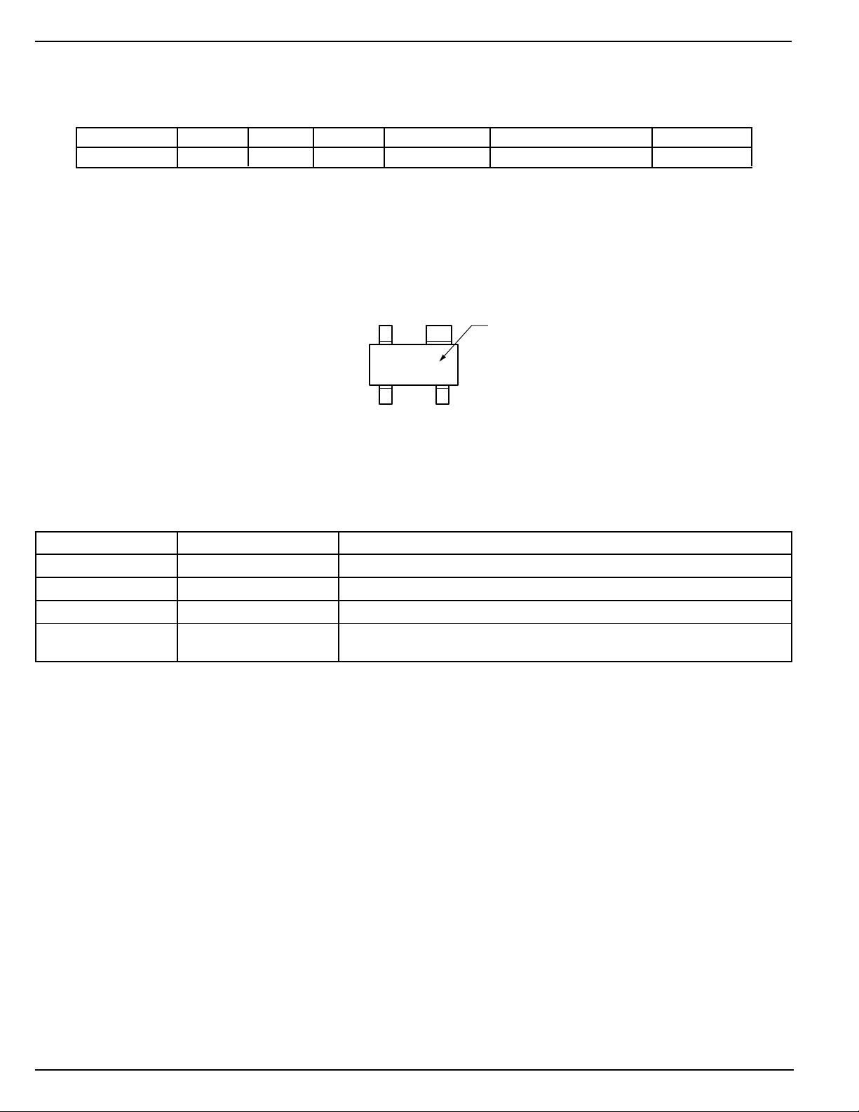
Pin Configuration
Pin Description
Pin Number Pin Name Pin Function
1 IN Input: Supply voltage input.
2 SNK Sink (Output): NPN open collector output.
3 GND Ground
4 FB Feedback (Input): 1.245V feedback input from external voltage-divider
FB GND
RBxx
12
IN
MIC4043
network.
34
SNK
Part
Identification
Absolute Maximum Ratings (Note 1)
Input Voltage (VIN) ......................................................+15V
Output Voltage (V
Storage Temperature (TS) ....................... –65°C to +150°C
ESD Rating, Note 3
) ................................................+15V
SNK
Operating Ratings (Note 2)
Input Voltage (VIN) ......................................................+10V
Output Voltage (V
Maximum Output Current (I
Temperature Range (TA) ........................... –40°C to +85°C
) ................................................+10V
SNK
) ................................15mA
SNK
human body model.................................................... 2kV
machine model........................................................200V
MIC4043 2 May 2000
Page 3
MIC4043 Micrel
Electrical Characteristics
TA = 25°C, bold values indicate –40°C ≤ TA ≤ +85°C; unless noted
Parameter Condition Min Typ Max Units
Reference Voltage 1.245 V
Reference Voltage Tolerance ±1%
±2 %
Supply Current I
Transconductance 1mA < I
∆I
/∆V
SINK
IN
Output Transistor I
Saturation Voltage 400 mV
Output Leakage V
Note 1. Exceeding the absolute maximum rating may damage the device.
Note 2. The device is not guaranteed to function outside its operating rating.
Note 3. Devices are ESD sensitive. Handling precautions recommended. Human body model, 1.5k in series with 100pF. Machine model, 200pF.
= 0mA 35 65 µA
SNK
70 µA
< 15mA 3.5 150 S
SNK
2 S
= 15mA 160 250 mV
SNK
= 5V, output transistor off 0.5 µA
SNK
1 µA
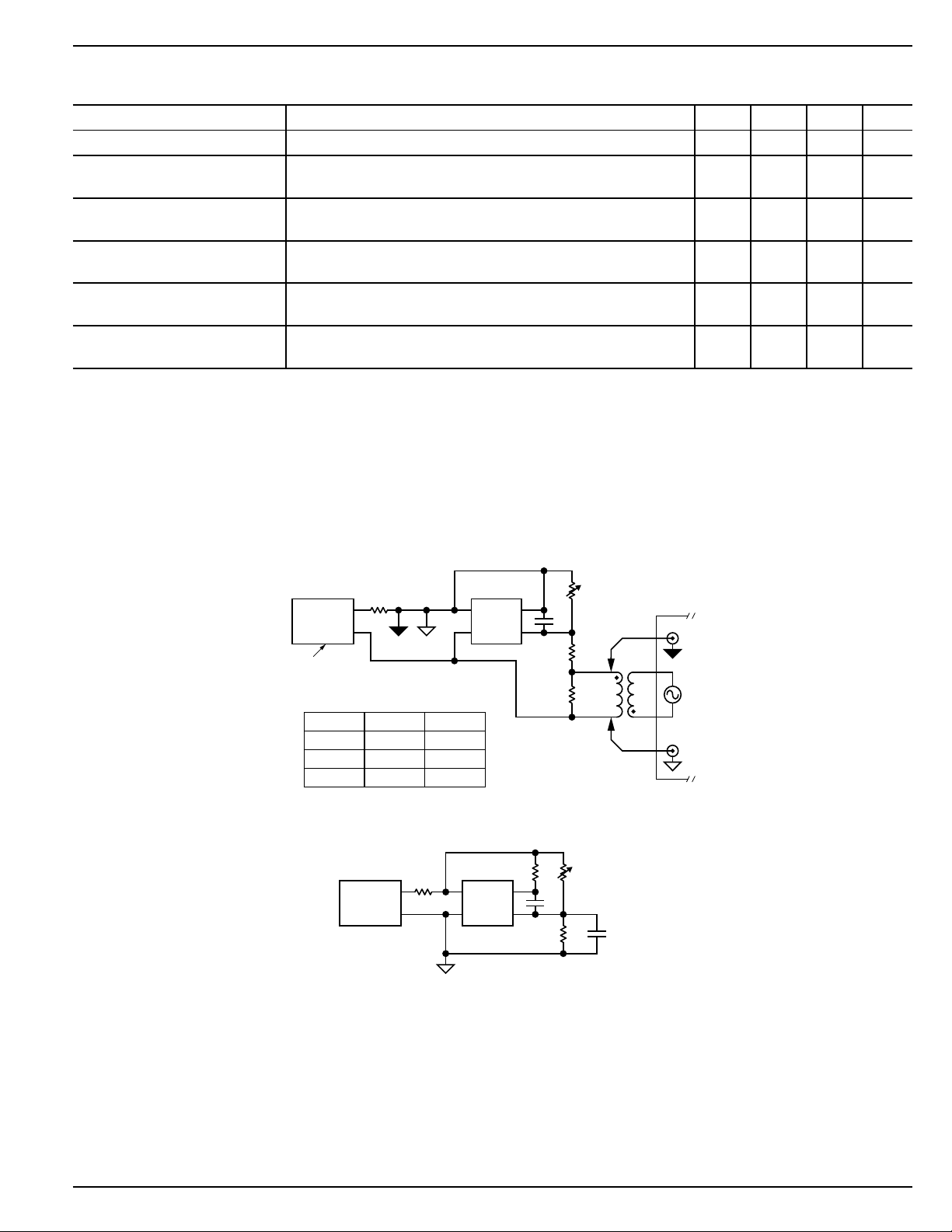
Test Circuits
Floating
Bench
Supply
RETURN
Do Not Ground!
V
V8.1k27k33
V5.2k33k33
V3.3k02k33
1k
R
* Compensation element
TUO
1R2R
MIC4043
SNKOUT
IN
GND FB
A
C
FB
2700pF
50Ω
Test Circuit 1. Compensation (Bode Plot) Circuit
Supply
RETURN
1k
MIC4043
IN
SNKOUT
GND FB
* Compensation components
R3
2k
C2*
2700pF
R2
33k
Test Circuit 2. Transient Response Circuit
R1
R1
R2
33k
R
A
C1*
1000pF
Analyzer
R
R
OUTPUT
A
A
May 2000 3 MIC4043
Page 4
MIC4043 Micrel
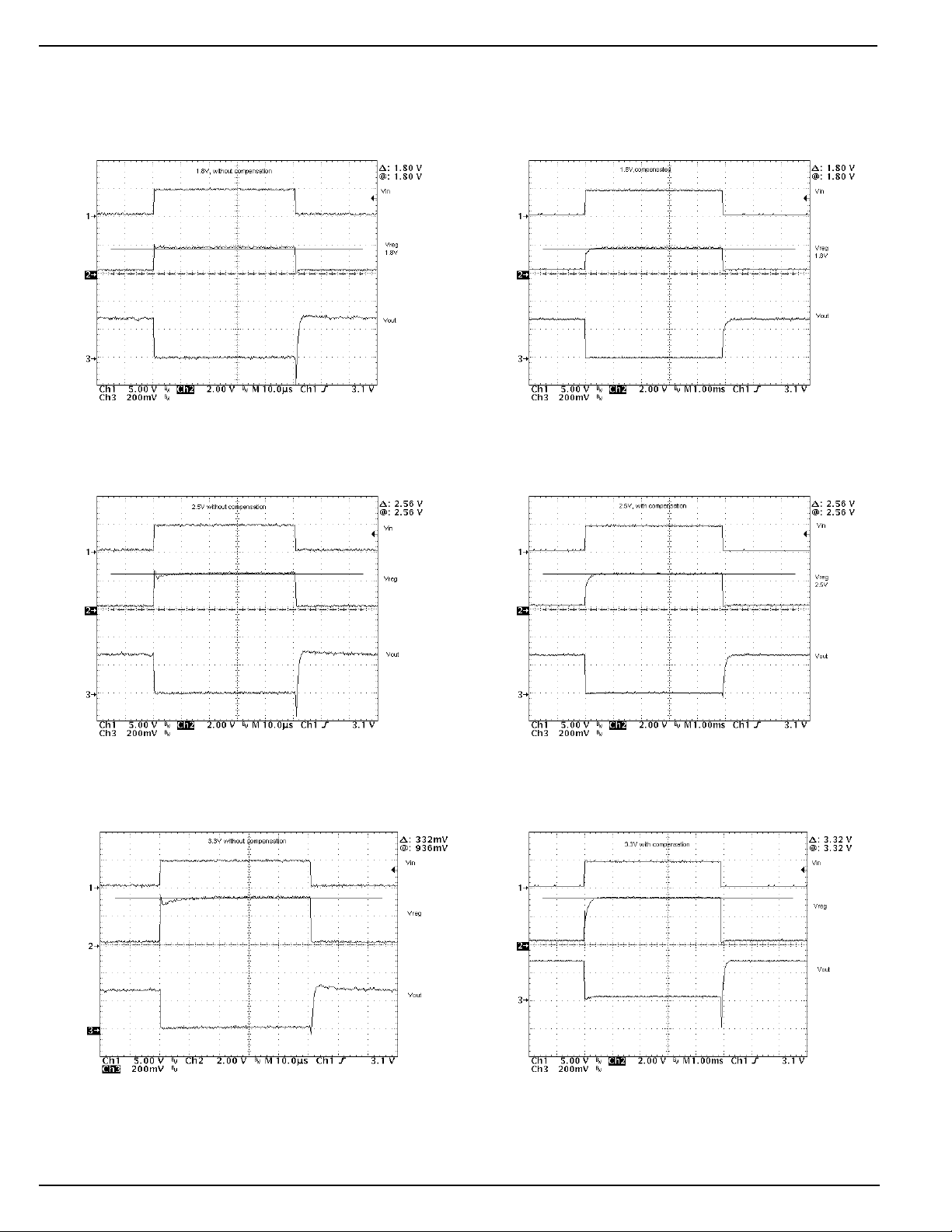
Transient Response 1a.
1.8V Output Without Compensation
IN
V
REG
V
OUT
V
V
V
V
IN
REG
OUT
Transient Response 2a.
2.5V Output Without Compensation
IN
V
IN
V
Transient Response 1b.
1.8V Output With Compensation
Transient Response 2b.
2.5V Output With Compensation
V
V
REG
OUT
V
V
V
IN
REG
OUT
Transient Response 3a.
3.3V Output Without Compensation
V
V
V
V
V
REG
OUT
Transient Response 3b.
3.3V Output With Compensation
IN
REG
OUT
MIC4043 4 May 2000
Page 5

MIC4043 Micrel
Functional Diagram
IN
V
REF
1.245V
SNK
FB
MIC4043
GND
Functional Description
The MIC4043 combines a Gm amplifier, precision 1.245V
reference, and a pass transistor in a single package.
The operation of the MIC4043 is similar to conventional shunt
regulators such as the industry standard ’431. In a closed
loop system, the MIC4043 maintains the desired feedback
voltage at the FB pin by sinking current onto the SNK pin
proportional to the error voltage at the FB pin. The ratio of sink
current to error voltage is the transconductance of the device.
Reference
The MIC4043 uses a
dividers providing feedback to the MIC4043 will be
high-side reference
. External voltage
inverted
when compared to those used with ’431-equivalent devices.
Behavior
The external feedback voltage is compared to the internal
high-side 1.245V reference.
If the feedback voltage, VFB, is less than VIN – V
REF
, the
amplifier provides no drive to the sink transistor. If the
feedback voltages is greater than VIN – V
, the amplifier
REF
drives the pass transistor which sinks current to ground.
May 2000 5 MIC4043
Page 6

MIC4043 Micrel
Applications Information
Replacement of ’431-Type Devices
Since the MIC4043 uses a high-side reference,
external
voltage dividers providing the feedback voltage will be
inverted when compared to those used with ’431-equiva-
lent devices.
The industry-standard ’431 is also typically used in series with
an opto-isolator LED. This configuration has a voltage drop of
at least 2.5V for the ’431 plus 1.4V for the LED (3.9V). More
recent lower-voltage shunt regulators require at least 1.25V
of headroom in addition to the 1.4V for the opto isolator, for
a total of 2.65V.
The MIC4043 effectively puts the regulator reference voltage
in parallel with the LED and drives the LED with a single,
series NPN transistor. The headroom required by this transistor is its saturation voltage of 400mV over it’s operating
temperature range, reducing the overall headroom requirement to 1.4V + 0.4V = 1.8V.
Compensation
The noninverting side of the error amplifier is connected to the
high-side reference; the reference is connected to the IN pin.
The inverting side of the error amplifier is brought out to the
FB pin. For some applications, no compensation is needed,
but for most, some small value of capacitance is necessary
between the FB pin and SNK pin. The value of the feedback
capacitance is application specific, but for most applications
100pF to 3000pF is all that is needed. Changing the feedback
capacitor changes the loop response; that is, phase and gain
margin. An empirical way to check overall system loop
response, if a network analyzer is not available, is to step load
the output of the systems from 10% to 100% of nominal load.
The resultant small signal response at the output of the
systems will provide an idea of which direction to go based on
the overshoot and settling time of V
OUT
.
Voltage Detector
R2
R1
R
PULL-UP
Logic
Output
1
DISABLED
ENABLED
=+
R1
R2
33k
V
OUT
POWER
SUPPLY)
(FROM
V 1.245V
TRIP
MIC4043
IN
SNK
GND FB
Figure 1. Voltage Detector
Figure 1 shows a simple voltage threshold detector with a
logic output.
High-Current Regulator
V
= 2.5VV
I
BIAS
≥500µA
IN
R
BIAS
MIC4043
SNK
IN
GND FB
Q1
OUT
V 1.245V
=+
OUT
R1 33k, R2 33k
∴= =
R1
33k
R2
33k
R2
1
R1
Figure 2. High-Current Regulator
For the high-current regulator shown in Figure 2, headroom
is equal to the saturation voltage of Q1 plus the saturation
voltage of the MIC4043 (V
SAT(min)
= 200mV).
MIC4043 6 May 2000
Page 7

MIC4043 Micrel
Off-Line 1.8V/2A Power Supply
85 to 264Vac
50/60Hz
Hot
Ground
Neutral
R5
1.21k 1%
R6
1.21k
1%
R7
14k 1%
C6
470pF
63V
U2a
2501
1
2
3
4
C7
470pF
63V
F1
1A
20mH
2200pF
C10
0.1µF
50/63V
U1
MIC38HC43BN
COMP
FB
I
SNS
RT/C
V
REF
V
V
OUT
GND
T
R1
1k 1%
L1
DD
C2
400V
8
7
6
5
0.1µF
250V
R2
332k
1%
R3
332k
1%
R13
10Ω 1%
C1
C3
2200pF
400V
D2
18V
R4
34Ω
1%
C5
0.1µF
50/
63V
IRFIBE30G
BR1
DBR1
47µF
400V
C8
22µF
25V
Q1
R8
1.9Ω
1/4W
1%
C4
1N4448
80T
D1
10T
1
2
4
3
C9
100pF
1kV
R9
470Ω
1/2W
MIC4043
12CTQ045
7
3T
6
T1
D3
UF4005
U2b
2501
U3
SNKIN
FBGND
D4
V 1.245V
TRIP
C14
50V
C13
1000pF
50/63V
R10
R15
47.5k
1%
R11
72k
1%
33k
1%
3000pF
L2
5µH
C11
1200µF
10V
=+
C12
220µF
10V
R2
1
R1
R12
90Ω
+1.8V/2A
R14
200Ω
1%
V
OUT
Return
Figure 3. Off-Line 1.8V/2A Power Supply
Figure 3a. 1.8V/1A Bode Plot
(θ margin = 69°)
Figure 3b. 1.8V/2A Bode Plot
(θ margin = 79°)
May 2000 7 MIC4043
Page 8

MIC4043 Micrel
Off-Line 2.5V/2A Power Supply
85 to 264Vac
50/60Hz
Hot
Ground
Neutral
R5
1.21k 1%
R6
1.21k
1%
R7
14k 1%
C6
470pF
63V
U2a
2501
1
2
3
4
C7
470pF
63V
F1
1A
20mH
2200pF
C10
0.1µF
50/63V
U1
MIC38HC43BN
COMP
FB
I
SNS
RT/C
V
REF
V
V
OUT
GND
T
R1
1k 1%
L1
DD
C2
400V
8
7
6
5
C1
0.1µF
250V
R2
332k
1%
R3
332k
1%
D2
18V
R13
10Ω 1%
C3
2200pF
400V
R4
34Ω
1%
C5
0.1µF
50/
63V
IRFIBE30G
BR1
DBR1
47µF
400V
C8
22µF
25V
Q1
R8
1.2Ω
1/4W
1%
C4
1N4448
75T
D1
1
2
4
9T
3
C9
100pF
1kV
R9
470Ω
1/2W
12CTQ045
7
3T
6
T1
D3
UF4005
U2b
2501
U3
MIC4043
SNKIN
FBGND
D4
V 1.245V
TRIP
C14
R10
3000pF
50V
C13
1000pF
50/63V
R15
47.5k
1%
R11
33k
1%
33k
1%
L2
5µH
C11
1200µF
10V
=+
C12
220µF
10V
R2
1
R1
R12
90Ω
+2.5V/2A
R14
200Ω
1%
V
OUT
Return
Figure 4. Off-Line 2.5V/2A Power Supply
Figure 4a. 2.5V/1A Bode Plot
(θ margin = 73°)
Figure 4b. 2.5V/2A Bode Plot
(θ margin = 65°)
MIC4043 8 May 2000
Page 9

MIC4043 Micrel
Off-Line 3.3V/2A Power Supply
C14
85 to 264Vac
50/60Hz
Hot
Ground
Neutral
R5
1.21k 1%
R6
1.21k
1%
R7
14k 1%
C6
470pF
63V
U2a
2501
1
2
3
4
C7
470pF
63V
F1
1A
20mH
2200pF
C10
0.1µF
50/63V
U1
MIC38HC43BN
COMP
FB
I
SNS
RT/C
V
REF
V
V
OUT
GND
T
R1
1k 1%
L1
DD
400V
8
7
6
5
C2
C1
0.1µF
250V
R2
332k
1%
R3
332k
1%
D2
18V
R13
10Ω 1%
C3
2200pF
400V
R4
34Ω
1%
C5
0.1µF
50/
63V
IRFIBE30G
BR1
DBR1
47µF
400V
C8
22µF
25V
Q1
R8
1.0Ω
1/4W
1%
C4
1N4448
77T
D1
10T
R9
470Ω
1/2W
1
2
4
3
C9
100pF
1kV
12CTQ045
7
3T
6
T1
D3
UF4005
U2b
2501
U3
MIC4043
SNKIN
FBGND
D4
V 1.245V
3000pF
L2
5µH
C11
1200µF
10V
=+
TRIP
50V
C13
1000pF
50/63V
R10
R15
47.5k
1%
R11
C12
220µF
10V
R2
R1
20k
1%
33k
1%
1
R12
90Ω
R14
200Ω
1%
V
OUT
+3.3V/2A
Return
Figure 5. Off-Line 3.3V/2A Power Supply
Figure 5a. 3.3V/1A Bode Plot
(θ margin = 76°)
Figure 5b. 3.3V/2A Bode Plot
(θ margin = 74°)
May 2000 9 MIC4043
Page 10

MIC4043 Micrel
Off-Line 5V/2A Power Supply
C14
85 to 264Vac
50/60Hz
Hot
Ground
Neutral
R5
1.21k 1%
R6
1.21k
1%
R7
14k 1%
C6
470pF
63V
U2a
2501
1
2
3
4
C7
470pF
63V
F1
1A
20mH
2200pF
C10
0.1µF
50/63V
U1
MIC38HC43BN
COMP
FB
I
SNS
RT/C
V
REF
V
V
OUT
GND
T
R1
1k 1%
L1
DD
C2
400V
8
7
6
5
C1
0.1µF
250V
R2
332k
1%
R3
332k
1%
D2
18V
R13
10Ω 1%
C3
2200pF
400V
R4
34Ω
1%
C5
0.1µF
50/
63V
IRFIBE30G
BR1
DBR1
47µF
400V
C8
22µF
25V
Q1
R8
0.68Ω
1/4W
1%
C4
1N4448
45T
D1
1
2
4
6T
3
C9
100pF
1kV
R9
470Ω
1/2W
U2b
2501
U3
MIC4043
SNKIN
D4
12CTQ045
7
3T
6
T1
Coiltronics
561-241-7876
D3
UF4005
3000pF
FBGND
L2
5µH
C11
1200µF
10V
V 1.245V
=+
TRIP
50V
C13
1000pF
50/63V
R15
47.5k
1%
R2
R1
R10
11k
1%
R11
33k
1%
C12
220µF
10V
1
R12
90Ω
R14
200Ω
1%
V
OUT
+5V/2A
Return
Figure 6. Off-Line 5V/2A Power Supply
Figure 6a. Off-Line 12V Input, 5V/2A Output Bode Plot
(θ margin = 83°)
MIC4043 10 May 2000
Page 11

MIC4043 Micrel
Package Information
0.950 (0.0374) TYP
C
L
3.05 (0.120)
2.67 (0.105)
0.800 (0.031) TYP
0.400 (0.016) TYP 3 PLACES
1.40 (0.055)
1.20 (0.047)
C
L
1.12 (0.044)
0.81 (0.032)
0.10 (0.004)
0.013 (0.0005)
2.50 (0.098)
2.10 (0.083)
DIMENSIONS:
MM (INCH)
8°
0°
0.150 (0.0059)
0.089 (0.0035)
0.41 (0.016)
0.13 (0.005)
SOT-143 (M4)
May 2000 11 MIC4043
Page 12

MIC4043 Micrel
MICREL INC. 1849 FORTUNE DRIVE SAN JOSE, CA 95131 USA
TEL + 1 (408) 944-0800 FAX + 1 (408) 944-0970 WEB http://www.micrel.com
This information is believed to be accurate and reliable, however no responsibility is assumed by Micrel for its use nor for any infringement of patents or
other rights of third parties resulting from its use. No license is granted by implication or otherwise under any patent or patent right of Micrel Inc.
© 2000 Micrel Incorporated
MIC4043 12 May 2000
 Loading...