

Datasheet MIC38C43-1BM, MIC38C43-1BN, MIC38C43BM, MIC38C43BMM, MIC38C42BN Datasheet (MICREL)
...Page 1
MIC38C42/3/4/5 Micrel
MIC38C42/3/4/5
BiCMOS Current-Mode PWM Controllers
General Description
The MIC38C4x are fixed frequency, high performance, current-mode PWM controllers. Micrel’s BiCMOS devices are
pin compatible with 384x bipolar devices but feature several
improvements.
Undervoltage lockout circuitry allows the ’42 and ’44 versions
to start up at 14.5V and operate down to 9V, and the ’43 and
’45 versions start at 8.4V with operation down to 7.6V. All
versions operate up to 20V.
When compared to bipolar 384x devices operating from a
15V supply, start-up current has been reduced to 50µA
typical and operating current has been reduced to 4.0 mA
typical. Decreased output rise and fall times drive larger
MOSFETs, and rail-to-rail output capability increases efficiency, especially at lower supply voltages. The MIC38C4x
also features a trimmed oscillator discharge current and
bandgap reference.
MIC38C4x denotes 8-pin plastic DIP, SOIC, and MM8™
packages. MIC38C4x-1 denotes 14-pin plastic DIP and
SOIC packages. 8-pin devices feature small size, while 14pin devices separate the analog and power connections for
improved performance and power dissipation.
Features
• Fast 40ns output rise and 30ns output fall times
• –40°C to +85°C temperature range
meets UC284x specifications
• High-performance, low-power BiCMOS Process
• Ultralow start-up current (50µA typical)
• Low operating current (4mA typical)
• CMOS outputs with rail-to-rail swing
• ≥ 500kHz current-mode operation
• Trimmed 5V bandgap reference
• Pin-for-pin compatible with UC3842/3843/3844/3845(A)
• Trimmed oscillator discharge current
• UVLO with hysteresis
• Low cross-conduction currents
Applications
• Current-mode, off-line, switched-mode power supplies
• Current-mode, dc-to-dc converters.
• Step-down “buck” regulators
• Step-up “boost” regulators
• Flyback, isolated regulators
• Forward converters
• Synchronous FET converters
For fast rise and fall times and higher output drive, refer to the
MIC38HC4x.
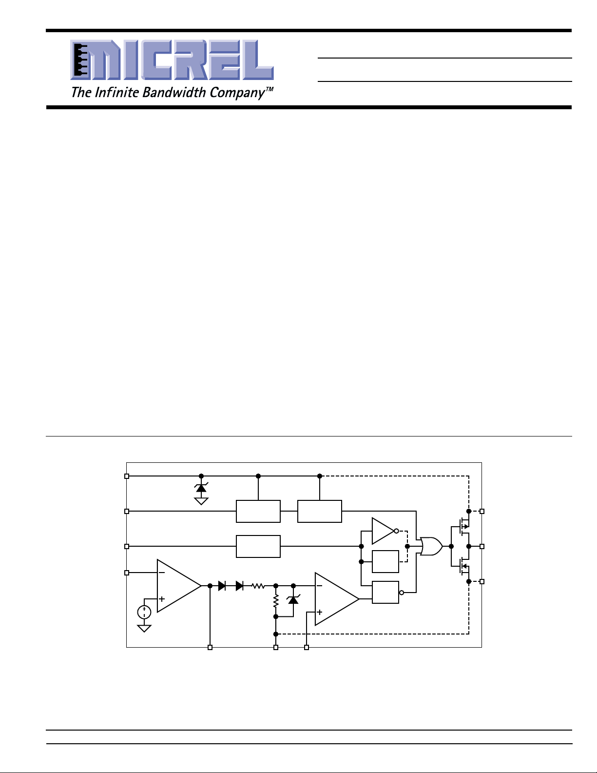
Functional Diagram
VDD
7 (12)
VREF
8 (14)
RT/CT
4 (7)
FB
2 (3)
2.5V
( ) pins are on MIC38C4x-1 (14-lead) versions only
* MIC38C4x (8-lead) versions only
†
MIC38C42, MIC38C43 (96% max. duty cycle) versions only
‡
MIC38C44, MIC38C45 (50% max. duty cycle) versions only
MM8 is a trademark of Micrel, Inc.
35V
COMP
1 (1)
5V
Reference
Oscillator
2R
R
GND*(AGND)
5 (9)
ISNS
3 (5)
UVLO
*
TQ
S
Q
R
*
(VD)
†
‡
(11)
OUT
6 (10)
(PGND)
(8)
Micrel, Inc. • 1849 Fortune Drive • San Jose, CA 95131 • USA • tel + 1 (408) 944-0800 • fax + 1 (408) 944-0970 • http://www.micrel.com
August 2000 1 MIC38C42/3/4/5
Page 2
MIC38C42/3/4/5 Micrel
Ordering Information
Part Number Temperature Range Package
MIC38C42BN –40°C to +85°C 8-pin Plastic DIP
MIC38C43BN –40°C to +85°C 8-pin Plastic DIP
MIC38C44BN –40°C to +85°C 8-pin Plastic DIP
MIC38C45BN –40°C to +85°C 8-pin Plastic DIP
MIC38C42-1BN –40°C to +85°C 14-pin Plastic DIP
MIC38C43-1BN –40°C to +85°C 14-pin Plastic DIP
MIC38C44-1BN –40°C to +85°C 14-pin Plastic DIP
MIC38C45-1BN –40°C to +85°C 14-pin Plastic DIP
MIC38C42BM –40°C to +85°C 8-pin SOIC
MIC38C43BM –40°C to +85°C 8-pin SOIC
MIC38C44BM –40°C to +85°C 8-pin SOIC
MIC38C45BM –40°C to +85°C 8-pin SOIC
MIC38C42BMM –40°C to +85°C 8-pin MM8™
MIC38C43BMM –40°C to +85°C 8-pin MM8™
MIC38C44BMM –40°C to +85°C 8-pin MM8™
MIC38C45BMM –40°C to +85°C 8-pin MM8™
MIC38C42-1BM –40°C to +85°C 14-pin SOIC
MIC38C43-1BM –40°C to +85°C 14-pin SOIC
MIC38C44-1BM –40°C to +85°C 14-pin SOIC
MIC38C45-1BM –40°C to +85°C 14-pin SOIC
Refer to the Part Number Cross Reference for a listings of Micrel devices equivalent to UC284x and UC384x devices.
Selection Guide
UVLO Thresholds
Startup 8.4V Startup 14.5V
Duty Cycle Minimum Operating 7.6V Minimum Operating 9V
0% to 96% MIC38C43 MIC38C42
0% to 50% MIC38C45 MIC38C44
MIC38C42/3/4/5 2 August 2000
Page 3
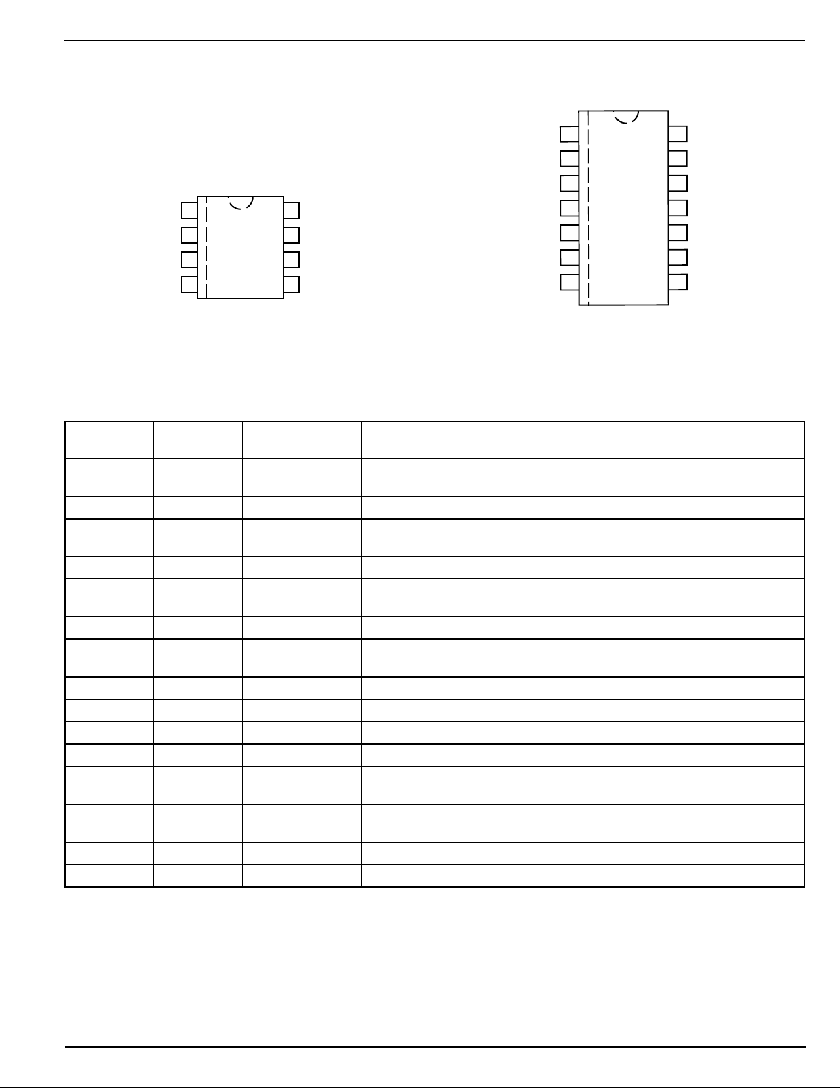
MIC38C42/3/4/5 Micrel
2NC NC13
3FB VDD12
4NC VD11
5ISNS OUT10
6NC AGND9
7RT/CT PGND8
1COMP VREF14
MIC38C4x-1
Pin Configuration
MIC38C4x
COMP
FB
ISNS
RT/CT
1
2
3
4
8
7
6
5
VREF
VDD
OUT
GND
8-Pin DIP (N)
8-Lead SOIC (M)
14-Pin DIP (-1BN)
14-Lead SOIC (-1BM)
8-Lead MM8™ (MM)
Pin Description
Pin Number Pin Number Pin Name Pin Function
N, M, MM -1BN, -1BM
1 1 COMP Compensation: Connect external compensation network to modify the error
amplifier output.
2 NC Not internally connected.
2 3 FB Feedback (Input): Error amplifier input. Feedback is 2.5V at desired output
voltage.
4 NC Not internally connected.
3 5 ISNS Current Sense (Input): Current sense comparator input. Connect to current
sensing resistor or current transformer.
6 NC Not internally connected.
4 7 RT/CT Timing Resistor/Timing Capacitor: Connect external RC network to select
switching frequency.
5 GND Ground: Combined analog and power ground.
8 PGND Power Ground: N-channel driver transistor ground.
9 AGND Analog Ground: Controller circuitry ground.
6 10 OUT Power Output: Totem-pole output.
11 VD Power Supply (Input): P-channel driver transistor supply input. Return to
power ground (PGND).
7 12 VDD Analog Supply (Input): Controller circuitry supply input. Return to analog
ground (AGND).
13 NC Not internally connected.
8 14 VREF 5V Reference (Output): Connect external RC network.
August 2000 3 MIC38C42/3/4/5
Page 4
MIC38C42/3/4/5 Micrel
Absolute Maximum Ratings
Zener Current (VDD) ...................................................30mA
Operation at
special precautions (Note 6).
Supply Voltage (V
DD
Switch Supply Voltage (VD) ..........................................20V
Current Sense Voltage (V
Feedback Voltage (V
Output Current, 38C42/3/4/5 (I
Storage Temperature (T
≥18V may require
), Note 6 .......................................20V
) ..................... –0.3V to 5.5V
ISNS
) ................................ –0.3V to 5.5V
FB
) ............................. 0.5A
OUT
) ....................... –65°C to +150°C
A
Operating Ratings
Junction Temperature (TJ) ........................................ 150°C
Package Thermal Resistance
8-Pin Plastic DIP (θ
8-Pin MM8™ (θJA) ............................................. 250°C/W
8-Pin SOIC (θJA) ...............................................170°C/W
14-Pin Plastic DIP (θJA) ....................................... 90°C/W
14-Pin SOIC (θJA) .............................................145°C/W
) ....................................... 125°C/W
JA
Electrical Characteristics
VDD = 15V, Note 4; RT = 11.0k; CT = 3.3nF; –40°C ≤ TA ≤ 85°C; unless noted
Parameter Test Conditions Min Typ Max Units
Reference Section
Output Voltage TA = 25°C, IO = 1mA 4.90 5.00 5.10 V
Line Regulation 12V ≤ VDD ≤ 18V, IO = 5µA, Note 6 220mV
Load Regulation 1 ≤ IO ≤ 20mA 1 25 mV
Temp. Stability Note 1 0.2 mV/°C
Total Output Variation Line, Load, Temp., Note 1 4.82 5.18 V
Output Noise Voltage 10Hz ≤ f ≤ 10kHz, TA = 25°C, Note 1 50 µV
Long Term Stability TA = 125°C, 1000 hrs., Note 1 525mV
Output Short Circuit –30 –80 –180 mA
Oscillator Section
Initial Accuracy TA = 25°C, Note 5 49 52 55 kHz
Voltage Stability 12 ≤ VDD ≤ 18V, Note 6 0.2 1.0 %
Temp. Stability T
Clock Ramp TA = 25°C, V
Reset Current TA = T
Amplitude V
Error Amp Section
Input Voltage V
Input Bias Current VFB = 5.0V –0.1 –2 µA
A
VOL
Unity Gain Bandwidth Note 1 0.7 1.0 MHz
≤ TA ≤ T
MIN
to T
MIN
peak to peak 1.9 Vp-p
RT/CT
= 2.5V 2.42 2.50 2.58 V
COMP
2 ≤ VO ≤ 4V 65 90 dB
, Note 1 0.04 %/°C
MAX
= 2V 7.7 8.4 9.0 mA
RT/CT
MAX
7.2 8.4 9.5 mA
PSRR 12 ≤ VDD ≤ 18V 60 dB
Output Sink Current VFB = 2.7V, V
Output Source Current VFB = 2.3V, V
V
High VFB = 2.3V, RL = 15k to ground 5 6.8 V
OUT
V
Low VFB = 2.7V, RL = 15k to V
OUT
= 1.1V 2 14 mA
COMP
= 5V –0.5 –1mA
COMP
REF
0.1 1.1 V
MIC38C42/3/4/5 4 August 2000
Page 5

MIC38C42/3/4/5 Micrel
Parameter Test Conditions Min Typ Max Units
Current Sense
Gain Notes 2, 3 2.85 3.0 3.15 V/V
MaximumThreshold V
= 5V, Note 2 0.9 1 1.1 V
COMP
PSRR 12 ≤ VDD ≤ 18V, Note 2 70 dB
Input Bias Current –0.1 –2 µA
Delay to Output 120 250 ns
Output
R
R
High I
DS(ON)
Low I
DS(ON)
SOURCE
SINK
= 200mA 20 Ω
= 200mA 11 Ω
Rise Time TA = 25°C, CL = 1nF 40 80 ns
Fall Time TA = 25°C, CL = 1nF 30 60 ns
Undervoltage Lockout
Start Threshold MIC38C42/4 13.5 14.5 15.5 V
MIC38C43/5 7.8 8.4 9.0 V
Minimum Operating Voltage MIC38C42/4 8 9 10 V
MIC38C43/5 7.0 7.6 8.2 V
Pulse Width Modulator
Maximum Duty Cycle MIC38C42/3 94 96 %
MIC38C44/5 46 50 %
Minimum Duty Cycle 0%
Total Standby Current
Start-Up Current VDD = 13V for MIC38C42/44 50 200 µA
VDD = 7.5V for MIC38C43/45
Operating Supply Current VFB = V
Zener Voltage (VDD)I
= 25mA, Note 6 30 37 V
DD
= 0V 4.0 6.0 mA
ISNS
Note 1: These parameters, although guaranteed, are not 100% tested in production.
Note 2: Parameter measured at trip point of latch with VEA = 0.
Note 3: Gain defined as:
∆
V
PIN1
A =
V (I )
TH
; ≤≤
0 V (I ) 0.8V
TH
SNS
SNS
Note 4: Adjust VDD above the start threshold before setting at 15V.
Note 5: Output frequency equals oscillator frequency for the MIC38C42 and MIC38C43. Output frequency for the MIC38C44, and
MIC38C45 equals one half the oscillator frequency.
Note 6: On 8-pin version, 20V is maximum input on pin 7, as this is also the supply pin for the output stage. On 14-pin version, 40V is
maximum for pin 12 and 20V maximum for pin 11.
August 2000 5 MIC38C42/3/4/5
Page 6

MIC38C42/3/4/5 Micrel
Typical Characteristics
Oscillator Frequency
100
RESISTANCE (kΩ)
R
10
T
1x10
Configuration
200pF
470pF
1.8nF
4.7nF
10nF
VDD = 15V
1
4
OSCILLATOR FREQUENCY (Hz)
1x10
5
1nF
5x10
Current Sense Amplifier
vs. Error Amplifier Output
1.2
1.0
0.8
0.6
0.4
0.2
0.0
CURRENT SENSE AMP THRESHOLD (V)
125°C
25°C
-50°C
02468
ERROR AMPLIFIER OUTPUT (V)
MIC38C42/43 Output Dead Time
vs. Oscillator Frequency
100
VDD = 15V
4.7nF
10
10nF
OUTPUT DEAD TIME (%)
5
1
1x10
4
FREQUENCY (Hz)
1x10
18nF
5
1nF
200pF
470pF
1x10
6
Short-Circuit Reference
Current vs. Temperature
120
100
80
60
40
VDD = 15V
20
SHORT CURCUIT CURRENT (mA)
0
REF
-60 -30 0 30 60 90 120 150
V
TEMPERATURE (°C)
Oscillator Discharge
Current vs. Temperature
9.0
8.8
8.6
8.4
8.2
8.0
7.8
7.6
7.4
7.2
7.0
OSC. DISCHARGE CURRENT (mA)
-60 -30 0 30 60 90 120 150
TEMPERATURE (°C)
VDD = 15V
V
= 2V
OSC
MIC38C4x
Output Waveform
25
20
15
10
5
0
-5
VD = 15V
OUTPUT VOLTAGE (V)
-10
C
= 1nF
L
-15
0.0 0.2 0.4 0.6 0.8 1.0
TIME (µs)
MIC38C42/3/4/5 6 August 2000
Page 7

MIC38C42/3/4/5 Micrel
Application Information
Familiarity with 384x converter designs is assumed.
The MIC38C4x has been designed to be compatible with
384xA series controllers.
MIC38C4x Advantages
Start-up Current
Start-up current has been reduced to an ultra-low 50µA
(typical) permitting higher-valued, lower-wattage, start-up
resistors (powers controller during power supply start-up).
The reduced resistor wattage reduces cost and printed circuit
space.
Operating Current
Operating current has been reduced to 4mA compared to
11mA for a typical bipolar controller. The controller runs
cooler and the VDD hold-up capacitance required during
start-up may be reduced.
Output Driver
Complementary internal P- and N-channel MOSFETs produce rail-to-rail output voltages for better performance driving
external power MOSFETs. The driver transistor’s low onresistance and high peak current capability can drive gate
capacitances of greater than 1000pF. The value of output
capacitance which can be driven is determined only by the
rise/fall time requirements. Within the restrictions of output
capacity and controller power dissipation, maximum switching frequency can approach 500kHz.
Design Precautions
When operating near 20V, circuit transients can easily exceed the 20V absolute maximum rating, permanently damaging the controller’s CMOS construction. To reduce transients, use a 0.1µF low-ESR capacitor to next to the controller’s
supply V
(or VD for ‘-1’ versions) and ground connections.
DD
Film type capacitors, such as Wima MKS2, are recommended.
When designing high-frequency converters, avoid capacitive
and inductive coupling of the switching waveform into highimpedance circuitry such as the error amplifier, oscillator, and
current sense amplifier. Avoid long printed-circuit traces and
component leads. Locate oscillator and compensation circuitry near the IC. Use high frequency decoupling capacitors
on V
, and if necessary, on VDD. Return high di/dt currents
REF
directly to their source and use large area ground planes.
Buck Converter
Refer to figure 1. When at least 26V is applied to the input,
C5 is charged through R2 until the voltage VDD is greater than
14.5V (the undervoltage lockout value of the MIC38C42).
Output switching begins when Q1 is turned on by the gate
drive transformer T1, charging the output filter capacitor C3
through L1. D5 supplies a regulated +12V to VDD once the
circuit is running.
Current sense transformer CT1 provides current feedback to
ISNS for current-mode operation and cycle-by-cycle current
limiting. This is more efficient than a high-power sense
resistor and provides the required ground-referenced level
shift.
When Q1 turns off, current flow continues from ground
through D1 and L1 until Q1 is turned on again.
The 100V Schottky diode D1 reduces the forward voltage
drop in the main current path, resulting in higher efficiency
than could be accomplished using an ultra-fast-recovery
diode. R1 and C2 suppress parasitic oscillations from D1.
Using a high-value inductance for L1 and a low-ESR capacitor for C3 permits small capacitance with minimum output
V
IN
26V to 40V
D2
M17Z105
1/4W
R2
68k
D3
MBR030
6.8k
0.22µF
R4
18
100k
CT1
0.1µF*
MIC38C42
1
COMP
2
FB
3
ISNS
4
RT/CT GND
C7
200pF
MKS2
VREF
VDD
OUT
R5
16k
8
7
6
5
0.1µF
C5
4.7µF
C8
0.1µF
D4
1N765B
4.7Ω
0.1µF
T1
Q1
IRF820
C2
L1 48µH
31DQ10
D1
R1
10
1/2W
1000pF
*Locate near MIC38C42 supply pins
C3
3.3µFC40.1µF
D5
1N4001
6.19k
1%
1.62k
1%
V
OUT
12V, 2A
Figure 1. 500kHz, 25W, Buck Converter
August 2000 7 MIC38C42/3/4/5
Page 8

MIC38C42/3/4/5 Micrel
ripple. This inductance value also improves circuit efficiency
by reducing the flux swing in L1.
Magnetic components are carefully chosen for minimal loss
Test Conditions Results
Line Regulation VIN = 26V to 80V, IO = 2A 0.5%
Load Regulation VIN = 48V, IO = 0.2A to 2A 0.6%
Efficiency VIN = 48V, IO = 2A 90%
Output Ripple VIN = 48V, IO = 2A (20MHz BW) 100mV
Synchronous Buck Converter
Refer to figure 2. This MIC38C43 synchronous buck converter uses an MIC5022 half-bridge driver to alternately drive
the PWM switch MOSFET (driven by GATEH, or high-side
output) and a MOSFET which functions as a synchronous
rectifier (driven by the GATEL, or low-side output).
The low-side MOSFET turns on when the high-side MOSFET
is off, allowing current to return from ground. Current flows
through the low-side MOSFET in the source to drain direction.
+12V
at 500kHz. CT1 and T1 are wound on Magnetics, Inc. P-type
material toroids. L1 is wound on a Siemens N49 EFD core.
Symbol Custom Coil
1
CT1 4923 ETS 92420
T1 4924 ETS 92419
L1 4925 ETS 92421
1. Custom Coils, Alcester, SD tel: (605) 934-2460
2. Energy Transformation Systems, Inc. tel: (415) 324-4949.
ETS
2
The on-state voltage drop of the low-side MOSFET is lower
than the forward voltage drop of an equivalent Schottky
rectifier. This lower voltage drop results in higher efficiency.
A sense resistor (5mΩ) is connected to the driver’s high-side
current sense inputs to provide overcurrent protection. Refer
to the MIC5020, MIC5021, and MIC5022 data sheets for
more information.
6.8k
2200
pF
10k
47k
3.3k
300k
10k
4.3k
0.15µF
4.7nF
MIC5022
VDD
0.1µF
MIC38C43
VREF
COMP
FB
ISNS
RT/CT
VDD
VOUT
GND
*Locate near the MIC38C43 supply pins.
470µF
0.1µF*
MKS2
25V
NC
NC
NC
FLT
EN
IN
CT
GND
GATEH
GATEL
SH+
SH–
SL+
SL–
Figure 2. 100kHz, Synchronous Buck Converter
VB
0.1µF
SMP60N06-14
5mΩ
35µH
V
OUT
5V, 8A
1000µF
Low ESR
MIC38C42/3/4/5 8 August 2000
Page 9

MIC38C42/3/4/5 Micrel
Package Information
PIN 1
DIMENSIONS:
INCH (MM)
.235 (5.969)
.215 (5.461)
.160 MAX
(4.064)
0.018 (0.57)
0.100 (2.54)
0.380 (9.65)
0.370 (9.40)
8-Pin Plastic DIP (N)
.770 (19.558) MAX
.060 (1.524)
.045 (1.143)
0.135 (3.43)
0.125 (3.18)
0.130 (3.30)
0.0375 (0.952)
0.255 (6.48)
0.245 (6.22)
0.300 (7.62)
0.013 (0.330)
0.010 (0.254)
0.380 (9.65)
0.320 (8.13)
PIN 1
.310 (7.874)
.280 (7.112)
.080 (1.524)
.015 (0.381)
.160 (4.064)
.100 (2.540)
.110 (2.794)
.090 (2.296)
.060 (1.524)
.045 (1.143)
.023 (.5842)
.015 (.3810)
14-Pin Plastic DIP (N)
.015 (0.381)
.008 (0.2032)
.400 (10.180)
.330 (8.362)
August 2000 9 MIC38C42/3/4/5
Page 10

MIC38C42/3/4/5 Micrel
0.026 (0.65)
MAX)
PIN 1
0.157 (3.99)
0.150 (3.81)
0.064 (1.63)
0.045 (1.14)
0.122 (3.10)
0.112 (2.84)
0.036 (0.90)
0.032 (0.81)
0.050 (1.27)
TYP
0.197 (5.0)
0.189 (4.8)
8-Pin SOP (M)
0.199 (5.05)
0.187 (4.74)
0.120 (3.05)
0.116 (2.95)
0.020 (0.51)
0.013 (0.33)
0.0098 (0.249)
0.0040 (0.102)
0°–8°
SEATING
PLANE
0.043 (1.09)
0.038 (0.97)
0.012 (0.30) R
DIMENSIONS:
INCHES (MM)
0.050 (1.27)
0.016 (0.40)
0.244 (6.20)
0.228 (5.79)
45°
0.010 (0.25)
0.007 (0.18)
DIMENSIONS:
INCH (MM)
0.007 (0.18)
0.005 (0.13)
0.012 (0.03)
0.0256 (0.65) TYP
0.154 (3.90)
0.026 (0.65)
MAX)
0.057 (1.45)
0.049 (1.25)
0.050 (1.27)
TYP
0.344 (8.75)
0.337 (8.55)
0.008 (0.20)
0.004 (0.10)
8-Pin MSOP (MM)
PIN 1
0.016 (0.40)
TYP
0.006 (0.15)
SEATING
PLANE
14-Pin SOP (M)
5° MAX
0° MIN
DIMENSIONS:
INCHES (MM)
0.012 (0.03) R
0.039 (0.99)
0.035 (0.89)
0.021 (0.53)
0.193 (4.90)
45°
3°–6°
0.244 (6.20)
0.228 (5.80)
MIC38C42/3/4/5 10 August 2000
Page 11

MIC38C42/3/4/5 Micrel
August 2000 11 MIC38C42/3/4/5
Page 12

MIC38C42/3/4/5 Micrel
MICREL INC. 1849 FORTUNE DRIVE SAN JOSE, CA 95131 USA
TEL + 1 (408) 944-0800 FAX + 1 (408) 944-0970 WEB http://www.micrel.com
This information is believed to be accurate and reliable, however no responsibility is assumed by Micrel for its use nor for any infringement of patents or
other rights of third parties resulting from its use. No license is granted by implication or otherwise under any patent or patent right of Micrel Inc.
© 2000 Micrel Incorporated
MIC38C42/3/4/5 12 August 2000
 Loading...