

Page 1
MIC2981/2982 Micrel
MIC2981/2982
High-Voltage High-Current Source Driver Array
Preliminary Information
General
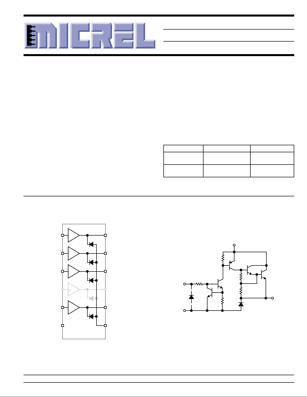
The MIC2981/82 is an 8-channel, high-voltage, high-current
source driver array ideal for switching high-power loads from
logic-level TTL, CMOS, or PMOS control signals.
These drivers can manage multiple loads of up to 50V and
500mA, limited only by package power dissipation.
Micrel’s MIC2981/82 features inputs compatible with 5V TTL
and 5V to 15V CMOS or PMOS logic outputs. Micrel’s dualmarked device replaces either UDN2981 or UDN2982 devices.
The MIC2981/82 is available in the 18-pin plastic DIP and 18lead wide SOP package. Both devices operate in the industrial temperature range.
Functional Diagrams
Features
• Output voltage to 50V
• Output current to 500mA
• Transient-protected outputs
• Integral clamp diodes
• TTL, CMOS, or PMOS compatible inputs
Applications
• Relay and solenoid switching
• Stepping motor
• LED and incandescent displays
Ordering Information
Part Number Temperature Range Package
MIC2981BN/
MIC2982BN* –40°C to +85°C 18-pin DIP
MIC2981BWM/
MIC2982BWM* –40°C to +85°C 18-pin wide SOP
* Orders for MIC2981BN or MIC2982BN will be filled with dual-marked
MIC2981/82BN. Orders for MIC2981BWM or MIC2982BWM will be
filled with dual-marked MIC2981/82BWM.
IN1
IN2
IN3
IN4–IN7
IN8
Micrel, Inc. • 1849 Fortune Drive • San Jose, CA 95131 • USA • tel + 1 (408) 944-0800 • fax + 1 (408) 944-0970 • http://www.micrel.com
4
S
MIC2981
MIC2982
OUT1
OUT2
OUT3
OUT4–OUT7
OUT8
GNDV
V
S
20k
1.8k
IN
1.5k
GND
Typical MIC2891/2982 Source Driver
800Ω
OUT
November 1999 1 MIC2981/2982
Page 2
MIC2981/2982 Micrel
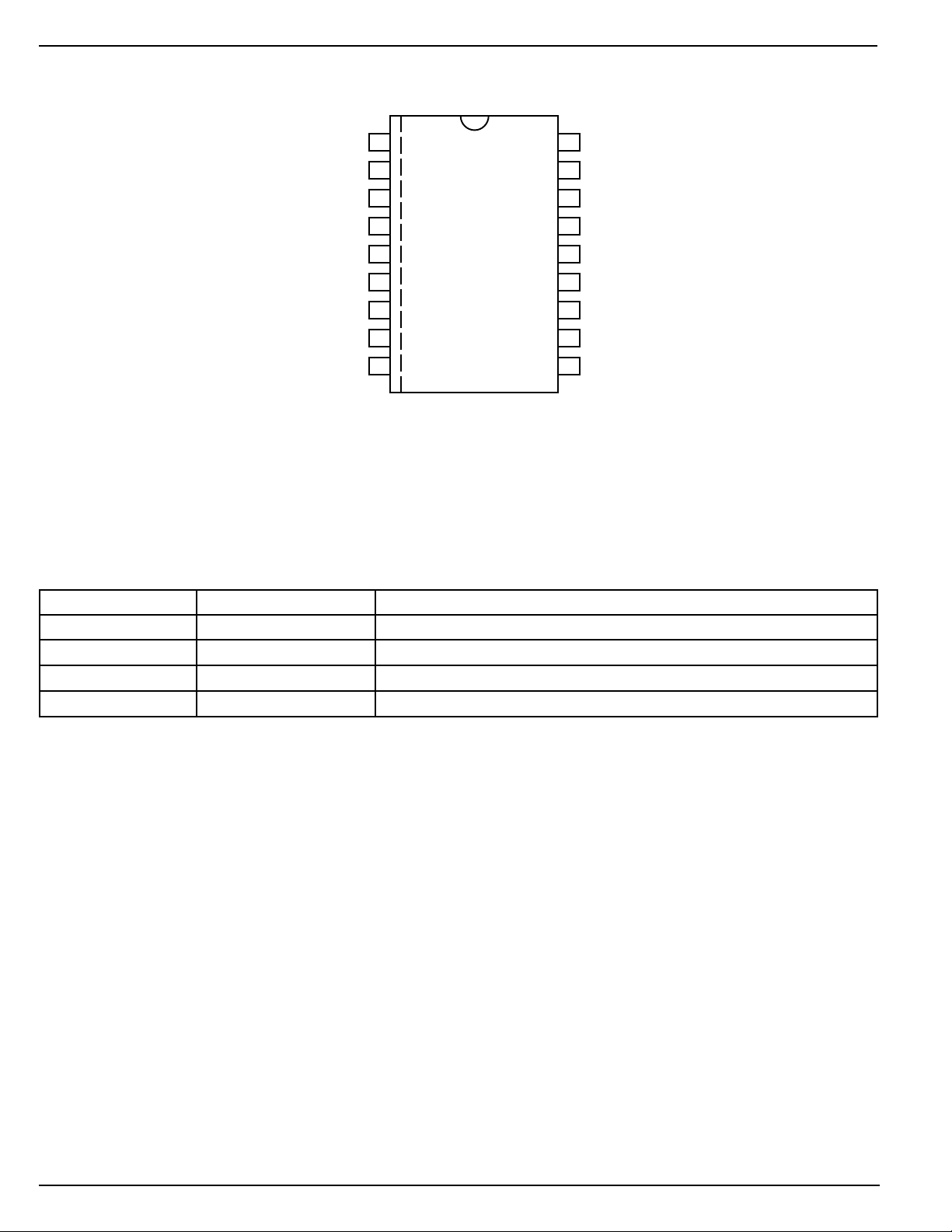
Pin Configuration
1IN1 OUT118
2IN2 OUT217
3IN3 OUT316
4IN4 OUT415
5IN5 OUT514
6IN6 OUT613
7IN7 OUT712
8IN8 OUT811
Pin Description
Pin No. Pin No. Pin Name Pin Function
1–8 IN1–IN8 Input 1 through Input 8: Base drive to driver input transistor.
9V
10 GND Ground
11–18 OUT8–OUT1 Output 8 through Output 1: Emitter of Darlington driver output.
9V
S
GND10
18-Pin DIP (N)
18-Pin Wide SOP (WM)
S
Supply Input
MIC2981/2982 2 November 1999
Page 3

MIC2981/2982 Micrel
Absolute Maximum Ratings
Supply Voltage (VS) ......................................................50V
Output Voltage (V
Continuous Output Current (I
Input Voltage (VIN)
MIC2981/82...............................................................30V
Ground Current (I
Junction Temperature (T
) ....................................................50V
CE
)................................500mA
C
) ....................................................3A
GND
) ......................................+150°C
J
Operating Ratings
Supply Voltage (VS) ............................................ 5V to 50V
Ambient Temperature (T
Package Thermal Resistance
PDIP θ
..............................................................56°C/W
JA
SOP θJA..............................................................84°C/W
)......................... –40°C to +85°C
A
Storage Temperature (TS) ....................... –65°C to +150°C
Electrical Characteristics
VS = 50V, TA = +25°C, unless noted.
Symbol Parameter Condition Min Typ Max Units
I
CEX
V
CE(sus)
V
CE(sat)
I
IN(on)
I
OUT
I
S
t
ON
t
OFF
I
R
V
F
General Note: Devices are ESD protected; however, handling precautions are recommended.
Note 1: Applied to all 8 inputs simultaneously.
Note 2: Load conditions affect turnoff delay.
Output Leakage Current VIN = 0.4V, TA = +70°C, Note 1 200 µA
Output Sustaining Voltage I
Collector-Emitter Saturation Voltage VIN = 2.4V, I
= 45mA 35 V
OUT
= 100mA 1.7 2.0 V
V
= 2.4V, I
IN
VIN = 2.4V, I
OUT
= 225mA 1.8 2.1 V
OUT
= 350mA 1.9 2.2 V
OUT
Input Current MIC2981 VIN = 2.4V 140 200 µA
VIN = 3.85 310 450 µA
MIC2982 V
= 2.4V 140 200 µA
IN
VIN = 12V 1.25 1.93 mA
Output Source Current VIN = 2.4V, VCE = 2.2V 350 mA
Supply Current VIN = 2.4, OUT1–8 = open, Note 1 10 mA
Turn-On Delay 0.5EIN to 0.5E
Turn-Off Delay 0.5EIN to 0.5E
Note 2
, RL = 100Ω, VS = 35V, 1.0 2.0 µs
OUT
, RL = 100Ω, VS = 35V, 5.0 10 µs
OUT
Clamp Diode Leakage Current VR = 50V, VIN = 0.4V, Note 1 50 µA
Clamp Diode Forward Voltage IF = 350mA 1.5 2.0 V
November 1999 3 MIC2981/2982
Page 4

MIC2981/2982 Micrel
Package Information
0.920
MAX
(23.370)
PIN 1
.250±0.005
(6.350±0.127)
0.060±0.005
(1.524±0.127)
0.130±0.005
(3.302±0.127)
0.020
MIN
(0.508)
0.301 (7.645)
0.297 (7.544)
0.040
(1.016)
0.018±0.003
(0.457±0.076)
0.100±0.010
(2.540±0.254)
18-Pin Plastic DIP (N)
TYP
PIN 1
0.030-0.110
(0.762-2.794)
0.020
(0.508)
0.125
MIN
(3.175)
DIMENSIONS:
INCHES (MM)
RAD
0.290-0.320
(7.336-8.128)
0°-10°
+0.025
0.325
–0.015
+0.635
8.255
()
–0.381
0.027 (0.686)
0.031 (0.787)
0.094 (2.388)
0.090 (2.286)
0.050 (1.270)
TYP
0.459 (11.659)
0.455 (11.557)
0.016 (0.046)
TYP
0.103 (2.616)
0.099 (2.515)
SEATING
PLANE
0.015
(0.381)
0.015
(0.381)
MIN
TYP
R
0.297 (7.544)
0.293 (7.442)
7°
0.330 (8.382)
0.326 (8.280)
0.032 (0.813) TYP
0.408 (10.363)
0.404 (10.262)
0.022 (0.559)
0.018 (0.457)
10° TYP
5°
TYP
18-Pin Wide SOP (WM)
MICREL INC. 1849 FORTUNE DRIVE SAN JOSE, CA 95131 USA
TEL + 1 (408) 944-0800 FAX + 1 (408) 944-0970 WEB http://www.micrel.com
This information is believed to be accurate and reliable, however no responsibility is assumed by Micrel for its use nor for any infringement of patents or
other rights of third parties resulting from its use. No license is granted by implication or otherwise under any patent or patent right of Micrel Inc.
© 1999 Micrel Incorporated
MIC2981/2982 4 November 1999
 Loading...