

Page 1
MIC29311 Micrel
MIC29311
3A Fast-Response LDO Regulator for USB
Preliminary Information
General Description
The MIC29311 is a 3A, fast response, low-dropout (LDO)
voltage regulator. Using Micrel’s proprietary Super βeta
PNP™ process, the MIC29311 offers exceptional dropout
(600mV at 3A) and low ground current (60mA at 3A). Fast
transient response allows it to recover quickly from large load
changes while maintaining a steady output. The device can
be sent into a “zero-current” off mode when the TTL compatible enable is brought low.
Designed specifically for Universal Serial Bus (USB) applications, the MIC29311 works with USB power switches to
provide an economical solution for self-powered hubs. The
5.1V output voltage is optimized to work with lower-cost high
on-resistance USB power switches (300mΩ) to provide a
minimum of 4.75V at 500mA to downstream ports. Used with
MIC2527 quad USB power switches, the MIC29311 can
power up to 6 downstream ports.
Features of the MIC29311 include thermal shutdown, current
limit, reversed-battery and reversed-lead insertion protection. An overvoltage clamp is available to maintain a safe
output when the input voltage exceeds 8V. An error flag is
also available to indicate of the output falls out of regulation,
or when an overcurrent condition occurs.
The MIC29311 is available in a 5-pin TO-220 or TO-263
package with a fixed 5.1V output voltage.
For other high current, low-dropout voltage regulators, please
see the MIC29150/300/500/750 and the MIC29310,
MIC29510, MIC29710.
Features
• Fast transient response
• 3A output current over full temperature range
• 600mV dropout voltage at full load
• Low ground current
• 3% total accuracy
• “Zero” off-mode current
• Thermal Shutdown
• Current Limiting
• Reversed battery protection
• Fixed 5.1V Output
Applications
• Self-powered USB hubs
• USB power switching
• High-efficiency linear power supplies
• High-efficiency switching supply post-regulator
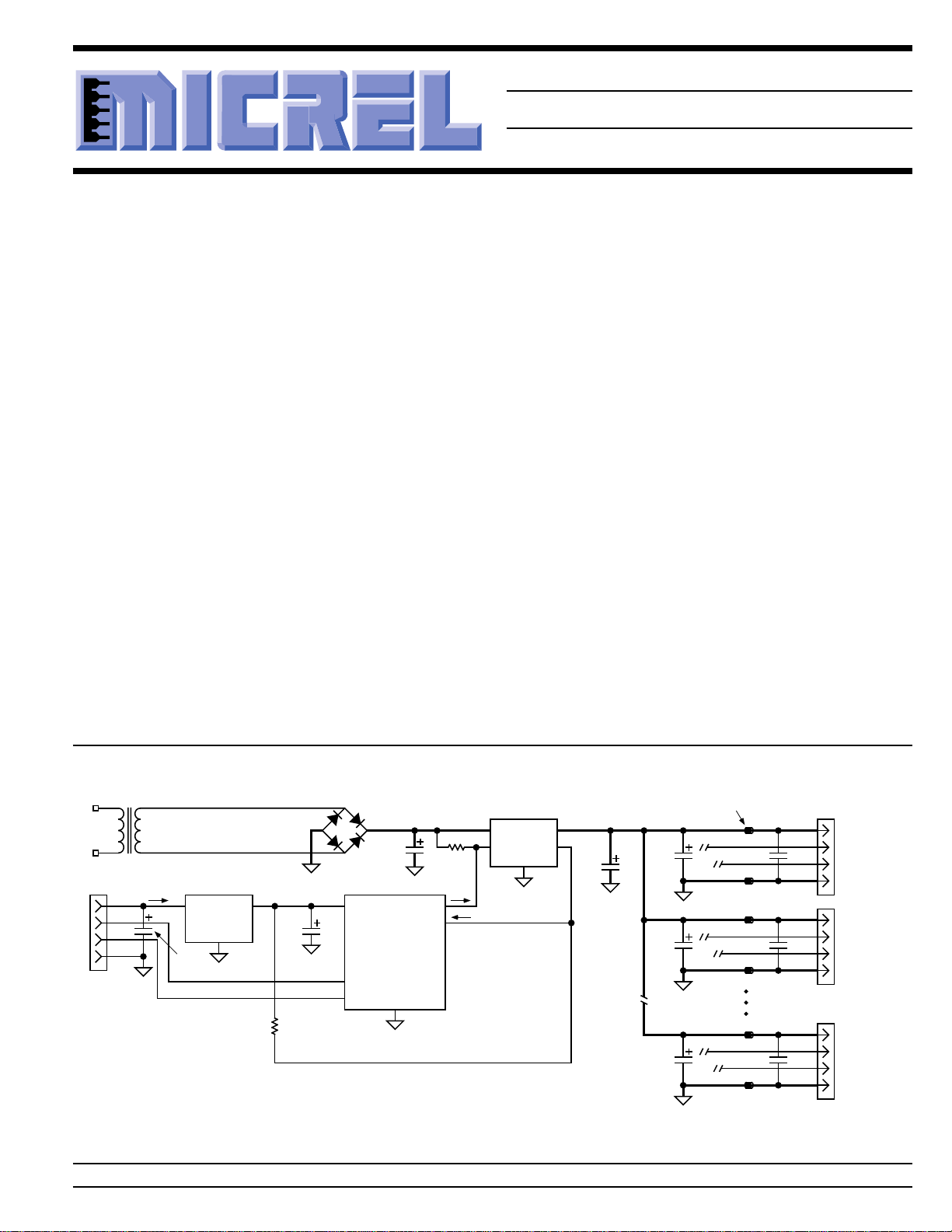
Typical Application
MIC29311-5.1
10k
LDO Regulator
IN OUT
FLAGEN
GND
33µF
33µF
33µF
33µF
AC
Line
100mA
V
BUS
D+
D–
GND
Upstream
USB Port
Bold lines indicate
0.1" wide, 1-oz. copper
high-current traces.
6.3Vac
3A
max.
MIC5207-3.3
LDO Regulator
IN OUT
GND
4.7
µF
10k
47µF
3.3V USB Controller
V+
1.0
OVERCURRENT
µF
D+
D–
GND
5.8V @ 3A 5.1V
ON/OFF
Simple USB Stand-Alone 6-Port Self-Powered Hub
Micrel, Inc. • 1849 Fortune Drive • San Jose, CA 95131 • USA • tel + 1 (408) 944-0800 • fax + 1 (408) 944-0970 • http://www.micrel.com
December 1998 1 MIC29311
Ferrite
Bead
0.01µF
0.01µF
0.01µF
V
BUS
D+
D–
GND
V
BUS
D+
D–
GND
V
BUS
D+
D–
GND
Downstream
USB
Port 1
4.75V min
500mA max.
Downstream
USB
Port 2
4.75V min
500mA max.
Downstream
USB
Port 6
4.75V min
500mA max.
Page 2
MIC29311 Micrel
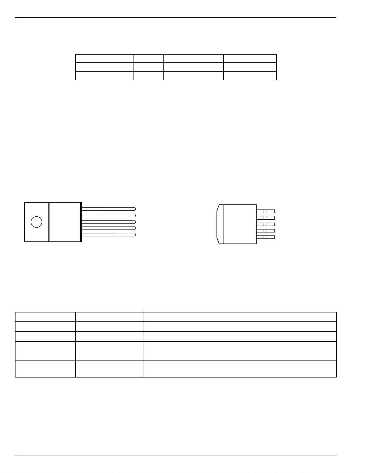
Ordering Information
Part Number Voltage Temperature Range Package
MIC29311-5.1BT 5.1V 0°C to +125°C TO-220-5
MIC29311-5.1BU 5.1V 0°C to +125°C TO-263-5
Pin Configuration
5 ERR
4 OUT
TAB
3 GND
2IN
1EN
TO-220-5 (T)
Pin Description
Pin Number Pin Name Pin Function
1 EN Enable (Input): Logic-level high enable/logic-level low shutdown control.
2 IN Unregulated Input: +16V maximum supply.
3, TAB GND Ground: Ground pin and TAB are internally connected.
4 OUT Regulator Output
5 ERR Error Flag (Output): Open-collector (active-low) output. Active low indicates
TAB
TO-263-5 (U)
overcurrent or undervoltage output conditions.
5 ERR
4 OUT
3 GND
2IN
1EN
MIC29311 2 December 1998
Page 3
MIC29311 Micrel
Absolute Maximum Ratings (Note 1)
Input Voltage (VIN) ........................................ –20V to +12V
Enable Voltage (VEN) .................................... –20V to +12V
Error Output Voltage (V
Lead Temperature (soldering, 5 sec.) ....................... 260°C
ESD Rating, Note 3
) ............................. 0V to +12V
ERR
Operating Ratings (Note 2)
Input Voltage (VIN) ........................................................+8V
Maximum Power Dissipation (P
Junction Temperature (TJ) ........................... 0°C to +125°C
Package Thermal Resistance
TO-220-5 (θJA) ....................................................55°C/W
)..................... Note 4
D(max)
TO-220-5 (θJC) ......................................................2°C/W
TO-263-5 (θJC) ......................................................2°C/W
Electrical Characteristics
TA = 25°C, bold values indicate 0°C ≤ TJ ≤ +125°C; unless noted.
Parameter Condition Min Typ Max Units
Output Tolerange 10mA ≤ I
Line Regulation I
= 10mA, (V
OUT
Load Regulation VIN = V
Output Voltage Temperature Note 5 20 100 ppm/°C
Coefficient
Dropout Voltage, Note 6 I
= 100mA 80 200 mV
OUT
I
= 750mA 220 mV
OUT
I
= 1.5A 330 mV
OUT
I
= 3A 600 1000 mV
OUT
Ground Current, Note 7 VIN = 6.1V, I
VIN = 6.1V, I
VIN = 6.1V, I
Dropout Ground Current VIN = 4.6V, I
Current Limit VIN = 3V, V
Minimum Load Current 710mA
Output Noise Voltage C
C
LOAD
LOAD
Error Flag Output
Output Leakage Current V
Output Low Voltage V
= 6.1V, V
IN
= 4.1V, I
IN
< 3A, (V
OUT
OUT
+ 1V, 10mA ≤ I
OUT
= 750mA 5 20 mA
OUT
= 1.5A 15 mA
OUT
= 3A 60 150 mA
OUT
= 10mA 2 3 mA
OUT
= 0V 3.0 3.8 A
OUT
+ 1V) ≤ VIN ≤ 8V –3 +3 %
OUT
+ 1V) ≤ VIN ≤ 8V 0.06 0.5 %
3A 0.2 1 %
OUT
= 10µF 400
= 33µF 260
= 8V 0.1 1 µA
ERR
= 250µA 220 300 mV
ERR
µV(rms)
µV(rms)
2 µA
400 mV
December 1998 3 MIC29311
Page 4

MIC29311 Micrel
Parameter Condition Min Typ Max Units
Enable Input
Logic Low Voltage regulator shutdown 0.8 V
Logic High Voltage regulator enabled 2.4 V
Enable Input Current V
= V
EN
IN
= 0.8V 2 µA
V
EN
Regulator Output Current VIN = ≤8V, VEN ≤ 0.8V (shutdown), V
Note 1. Exceeding the absolute maximum rating may damage the device.
Note 2. The device is not guaranteed to function outside its operating rating.
Note 3. Devices are ESD sensitive. Handling precautions recommended.
Note 4. P
Note 5. Output voltage temperature coefficient is defined as the ∆V
Note 6. VDO = VIN – V
Note 7. I
Note 8. VEN ≤ 0.8V and VIN ≤ 8V, V
= (T
D(max)
is the quiescent current. IIN = I
GND
– TA) ÷ θJA, where θJA depends upon the printed curcuit board layout. See “Applications Information.”
J(max)
when V
OUT
decreases to 99% of its nominal output voltage with VIN = V
OUT
OUT
= 0.
GND
+ I
OUT
.
OUT(worst case)
= 0V, Note 8 10 20 µA
OUT
÷ (T
J(max)
– T
J(min)
) where T
+ 1V.
OUT
is +125°C and T
J(max)
15 30 µA
75 µA
4 µA
is 0°C.
J(min)
MIC29311 4 December 1998
Page 5

MIC29311 Micrel
0
0.2
0.4
0.6
0.8
1.0
0 30 60 90 120 150
DROPOUT VOLTAGE (mV)
TEMPERATURE (°C)
0
50
100
150
200
0246810
GROUND CURRENT (mA)
INPUT VOLTAGE (V)
0
5
10
15
20
0 30 60 90 120 150
GROUND CURRENT (mA)
TEMPERATURE (°C)
0
1
2
3
4
5
6
0 30 60 90 120 150
CURRENT (A)
TEMPERATURE (°C)
Typical Characteristics
Dropout Voltage
vs. Output Current
0.6
0.5
0.4
0.3
0.2
0.1
DROPOUT VOLTAGE (V)
0.0
0123
OUTPUT CURRENT (A)
Ground Current
2.0
1.5
1.0
0.5
GROUND CURRENT (mA)
0.0
vs. Input Voltage
I
= 10mA
OUT
0246810
INPUT VOLTAGE (V)
MIC2931x Dropout Voltage
vs. Temperature
I
= 3A
LOAD
Ground Current
vs. Input Voltage
I
= 3A
OUT
Dropout
Characteristics
7
6
5
I
= 10mA
LOAD
Awaiting Further
4
Characterization
3
2
OUTPUT VOLTAGE (V)
1
0
0246
Data
I
= 3A
LOAD
INPUT VOLTAGE (V)
Ground Current
vs. Input Voltage
2.0
V
1.5
1.0
0.5
0.0
GROUND CURRENT (mA)
-0.5
= 3.3V
OUT
R
= 100Ω
LOAD
-20 -10 0 10 20
INPUT VOLTAGE (V)
6
5
4
3
2
1
GROUND CURRENT (mA)
0
0 30 60 90 120 150
vs. Output Current
60
50
40
December 1998 5 MIC29311
30
20
10
GROUND CURRENT (mA)
0
0123
OUTPUT CURRENT (A)
Ground Current
vs. Temperature
I
= 750mA
OUT
TEMPERATURE (°C)
Ground Current
Ground Current
vs. Temperature
I
= 1.5A
OUT
Output Voltage
5.20
5.18
5.16
5.14
5.12
5.10
5.08
5.06
5.04
OUTPUT VOLTAGE (V)
5.02
5.00
vs. Temperature
Awaiting Further
Characterization
Data
0 30 60 90 120 150
TEMPERATURE (°C)
Ground Current
100
GROUND CURRENT (mA)
vs. Temperature
80
60
40
20
0
0 30 60 90 120 150
I
= 3A
OUT
TEMPERATURE (°C)
Short Circuit
Current vs. Temperature
V
= 0V
OUT
Page 6

MIC29311 Micrel
0mA
200mA
3A
5.1V
+20mV
–20mV
LOAD CURRENT OUTPUT VOLTAGE
Load Transient Response
(See Test Circuit Schematic)
1ms/division
8.0V
6.0V
5.1V
+20mV
–20mV
OUTPUT VOLTAGE INPUT VOLTAGE
Line Transient Response
with 3A Load, 100µF Output Capacitance
200µs/division
I
OUT
= 3A
C
OUT
= 100µF
VIN = V
OUT
+ 1V
1µF
Enable Current
vs. Temperaure
40
35
30
25
20
15
10
ENABLE CURRENT (µA)
5
0
0 30 60 90 120 150
MIC29311-5.1
EN
IN
I
switching between 200mA and 3A
OUT
VEN = 5V
VEN = 2V
TEMPERATURE (°C)
OUT
ERR
GND
Error
Output
10k
V
OUT
5.1V nominal
330µF
4
AVX
TPSE337M006R0100
tantalum
OUTPUT IMPEDANCE (Ω)
0.001
0.1
0.01
Output Impedance
10
1
0
0
10x10
FREQUENCY (Hz)
vs. Frequency
3
3
1x10
100x10
10x10
3
100x10
6
1x10
Load Transcient Response Test Circuit
Line Transient Response
with 3A Load, 10µF Output Capacitance
8.0V
6.0V
200µs/division
+20mV
5.1V
–20mV
OUTPUT VOLTAGE INPUT VOLTAGE
= 3A
I
OUT
C
=10µF
OUT
MIC29311 6 December 1998
Page 7

MIC29311 Micrel
Reference
18V
O.V.
I
LIMIT
Thermal
Shutdown
1.240V
1.180V
EN
IN
FLAG
GND
OUT
R1*
R2*
Functional Diagram
December 1998 7 MIC29311
Page 8

MIC29311 Micrel
Applications Information
The MIC29311 is a high-performance low-dropout voltage
regulator suitable for all moderate to high-current voltage
regulator applications. The 600mV dropout voltage at full
load makes it especially valuable in battery-powered systems
and as high-efficiency noise filters in “post-regulator” applications. Its unique output voltage makes the MIC39311 ideal for
Universal Serical Bus (USB) power switching applications.
Unlike older NPN-pass transistor designs, where the minimum dropout voltage is limited by the base-emitter voltage
drop and collector-emitter saturation voltage, dropout performance of the PNP output of these devices is limited merely
by the low VCE saturation voltage.
A trade-off for the low dropout voltage is a varying base drive
requirement. But Micrel’s Super βeta PNP™ process reduces this drive requirement to merely 1% to 5% of the load
current.
The MIC29311 regulator is fully protected from damage due
to fault conditions. Current limiting is provided. This limiting is
linear; output current under overload conditions is constant.
Thermal shutdown disables the device when the die temperature exceeds the maximum safe operating temperature.
Transient protection allows device (and load) survival even
when the input voltage spikes above and below nominal. The
output structure of these regulators allows voltages in excess
of the desired output voltage to be applied without reverse
current flow. The MIC29311 version offers a logic level on-off
control: when disabled, the device draws nearly zero current.
MIC29311-5.1
Enable
Shutdown
V
IN
IN OUT
EN FLG Flag
GND
Figure 1. Input and Output Capacitors
Thermal Design
Linear regulators are simple to use. The most complicated
design parameters to consider are thermal characteristics.
Thermal design requires the following application-specific
parameters:
Maximum ambient temperature, T
Output Current, I
Output Voltage, V
Input Voltage, V
OUT
OUT
IN
First, calculate the power dissipation of the regulator from
these numbers and the device parameters from this datasheet.
P I 1.02V V
=−
D
()
OUT
IN
OUT
Where the ground current is approximated by 2% of I
Then the heat sink thermal resistance is determined by:
θθθ
TT
=
SA
Where T
J (max)
−
J(max) A
P
D
−+
JC CS
≤ 125°C and θCS is between 0 and 2°C/W.
V
OUT
A
OUT
The heat sink may be significantly reduced in applications
where the minimum input voltage is known and is large
compared with the dropout voltage. Use a series input
resistor to drop excessive voltage and distribute the heat
between this resistor and the regulator. The low dropout
properties of Micrel Super ßeta PNP regulators allow very
significant reductions in regulator power dissipation and the
associated heat sink without compromising performance.
When this technique is employed, a capacitor of at least 1µF
is needed directly between the input and regulator ground.
Please refer to Application Note 9 for further details and
examples on thermal design and heat sink specification.
Capacitor Requirements
For stability and minimum output noise, a capacitor on the
regulator output is necessary. The value of this capacitor is
dependent upon the output current; lower currents allow
smaller capacitors. The MIC29311 regulator is stable with a
minimum capacitor value of 10µF at full load.
This capacitor need not be an expensive low ESR type:
aluminum electrolytics are adequate. In fact, extremely low
ESR capacitors may contribute to instability. Tantalum capacitors are recommended for systems where fast load
transient response is important.
Where the regulator is powered from a source with a high AC
impedance, a 0.1µF capacitor connected between Input and
GND is recommended. This capacitor should have good
characteristics to above 250kHz. When the regulator is
located more than 3 inches from the ac bulk supply capacitors, a 1µF or greater input capacitor is recommended.
Minimum Load Current
The MIC29311 regulator is specified between finite loads. If
the output current is too small, leakage currents dominate
and the output voltage rises. A 10mA minimum load current
is necessary for proper regulation.
Enable Input
The MIC29311 version features an enable (EN) input that
allows on-off control of the device. Special design allows
“zero” current drain when the device is disabled—only microamperes of leakage current flows. The EN input has TTL/
CMOS compatible thresholds for simple interfacing with
logic, or may be directly tied to VIN. Enabling the regulator
requires approximately 20µA of current into the EN pin.
Error Flag
The MIC29311 features an error flag which looks at the output
voltage and signals an error condition when this voltage
drops 5% below its expected value. The error flag is an opencollector output that pulls low under fault conditions. It may
sink 10mA. Low output voltage signifies a number of possible
problems, including an overcurrent fault (the device is in
current limit) and low input voltage. The flag output is inopera-
.
tive during overtemperature shutdown conditions.
USB Applications
The main application of the MIC29311 is to control power
distribution in a self-powered Universal Serial Bus hub. For
self-powered hubs, the MIC29311 provides 5.1V ±3% to
downstream ports from an unregulated supply voltage (see
MIC29311 8 December 1998
Page 9

MIC29311 Micrel
“Typical Application”). USB requires that the downstream
voltage supplied to peripherals from a self-powered hub is
between 4.75V and 5.25V. The MIC29311 provides regulation with this requirement. The enable pin input controls
ganged power for up to seven downstream ports, each
drawing up to 500mA. The device has an output current
limiting circuit that linearly decreases the output voltage as
the output current exceeds 3A. When the part is out of
regulation by 5%, the error flag goes low and signals a fault
condition to the microcontroller, allowing the system to be
disabled. This provides the overcurrent protection that is
required by USB.
In Figure 2, the MIC29311 provides power to the MIC2527
quad power switches. The MIC2527 provides power switching to four independently controlled downstream ports. Two
MIC2527s can be used to provide a 6-port, self-powered hub
in conjunction with the MIC29311. The 5.1V output of the
MIC29311 is optimized to ensure that under maximum load
condition, the output voltage of each channel of the MIC2527
remains above 4.75V. This is the minimum voltage require-
ment for self-powered USB hubs. The output voltage is a
function of the minimum output voltage of the power supply,
the PCB trace resistance and the on-resistance of the switch.
Table 1 shows the maximum allowable on-resistance for a
5.1V power supply in a self-powered hub, assuming 30mV of
voltage drop due to PCB trace resistance. The 5.1V of the
MIC29311 and the 300mΩ on-resistance of each MIC2527
switch provides an economical solution to power management of self-powered hubs.
lanimoN
egatloV
V01.5
ylppuS
ecnareloT
muminiM
egatloV
mumixaM
egatloV
mumixaM
R
NO
%1V50.5V51.5m045 Ω
%2V5V2.5m044 Ω
%3 V59.4 V52.5 m043 Ω
%4V9.4V3.5—
%5V58.4V63.5—
Table 1. Max. Allowable On-Resistance
For further information concerning USB power management,
refer to Application Note 17 and Application Hint 30.
5.7V
MIC29311-5.1
LDO Regulator
IN OUT
EN ERR
GND
MIC5207-3.3
LDO Regulator
IN OUT
4.7
µF
GND
Bold lines indicate
0.1" wide, 1-oz. copper
high-current traces.
* 33µF, 16V tantalum or 100µF, 10V electrolytic per port
1µF
5.1V ±3%
V+
D+
D–
10k
ON/OFF
OVERCURRENT
GND
Figure 2. 4-Port Self-Powered Hub
47k
MIC25273.3V USB Controller
ENA
FLGA IN
ENB OUTA
FLGB
OUTB
ENC
OUTC
OUTDFLGC
END
FLGD GND
GND
Ferrite
Bead
33µF*
IN
0.1
µF
33µF*
33µF*
33µF*
0.01µF
0.01µF
0.01µF
0.01µF
4.75V min.
at 500mA
V
BUS
D+
D–
GND
V
BUS
D+
D–
GND
V
BUS
D+
D–
GND
V
BUS
D+
D–
GND
Downstream
USB
Port 1
500mA max.
Downstream
USB
Port 2
500mA max.
Downstream
USB
Port 3
500mA max.
Downstream
USB
Port 4
500mA max.
December 1998 9 MIC29311
Page 10

MIC29311 Micrel
Package Information
0.108 ±0.005
(2.74 ±0.13)
0.067 ±0.005
(1.70 ±0.127)
0.268 REF
(6.81 REF)
0.400 ±0.015
(10.16 ±0.38)
0.150 D ±0.005
(3.81 D ±0.13)
0.241 ±0.017
(6.12 ±0.43)
0.578 ±0.018
(14.68 ±0.46)
0.550 ±0.010
(13.97 ±0.25)
0.032 ±0.005
(0.81 ±0.13)
7°
Typ.
0.018 ±0.008
(0.46 ±0.20)
Dimensions:
0.177 ±0.008
(4.50 ±0.20)
0.050 ±0.005
(1.27 ±0.13)
SEATING
PLANE
0.103 ±0.013
(2.62±0.33)
inch
(mm)
TO-220-5 (T)
0.405±0.005
0.065±0.010
20°±2°
0.067±0.005 0.032 ±0.003
DIM. = INCH
0.050±0.005
0.360±0.005
TO-263-5 (U)
0.600±0.025
8° MAX
0.015 ±0.002
0.176±0.005
0.060±0.005
SEATING PLANE
+0.004
0.004
–0.008
0.100±0.01
MIC29311 10 December 1998
Page 11

MIC29311 Micrel
December 1998 11 MIC29311
Page 12

MIC29311 Micrel
MICREL INC. 1849 FORTUNE DRIVE SAN JOSE, CA 95131 USA
TEL + 1 (408) 944-0800 FAX + 1 (408) 944-0970 WEB http://www.micrel.com
This information is believed to be accurate and reliable, however no responsibility is assumed by Micrel for its use nor for any infringement of patents or
other rights of third parties resulting from its use. No license is granted by implication or otherwise under any patent or patent right of Micrel Inc.
© 1998 Micrel Incorporated
MIC29311 12 December 1998
 Loading...