

Page 1
MIC2561 Micrel
MIC2561
PCMCIA Card Socket VCC & VPP Switching Matrix
General Description
The MIC2561 VCC & VPP Matrix controls PCMCIA (Personal
Computer Memory Card International Association) memory
card power supply pins, both VCC and VPP. The MIC2561
switches voltages from the system power supply to VCC and
VPP. The MIC2561 switches between the three VCC voltages
(OFF, 3.3V and 5.0V) and the VPP voltages (OFF, 0V, 3.3V,
5V, or 12.0V) required by PCMCIA cards. Output voltage is
selected by two digital inputs for each output and output
current ranges up to 750mA for VCC and 200mA for VPP. For
higher VCC output current, please refer to the full-performance MIC2560.
The MIC2561 provides power management capability under
the control of the PC Card controller and features overcurrent
and thermal protection of the power outputs, zero current
“sleep” mode, suspend mode, low power dynamic mode, and
ON/OFF control of the PCMCIA socket power.
The MIC2561 is designed for efficient operation. In standby
(“sleep”) mode the device draws very little quiescent current,
typically 0.01µA. The device and PCMCIA port is protected by
current limiting and overtemperature shutdown. Full crossconduction lockout protects the system power supply.
Ordering Information
Part Number Temperature Range Package
MIC2561-0BM 0°C to +70°C 14-pin SOIC
Applications
• PCMCIA Power Supply Pin Voltage Switch
• Data Collection Systems
• Machine Control Data Input Systems
• Wireless Communications
• Bar Code Data Collection Systems
• Instrumentation Configuration/Datalogging
• Docking Stations (portable and desktop)
• Power Supply Management
• Power Analog Switching
Features
• Complete PCMCIA VCC and VPP Switch Matrix in a
Single IC
• No External Components Required
• Controlled Switching Times
• Logic Options for Compatible with Industry Standard
PCMCIA Controllers
• No Voltage Overshoot or Switching Transients
• Break-Before-Make Switching
• Output Current Limit and Over-Temperature Shutdown
• Digital Flag for Error Condition Indication
• Ultra Low Power Consumption
• Digital Selection of VCC and VPP Voltages
• Over 750mA of VCC Output Current
• 200mA of VPP Output Current
• 14-Pin SOIC Package
MIC2561-1BM 0°C to +70°C 14-pin SOIC
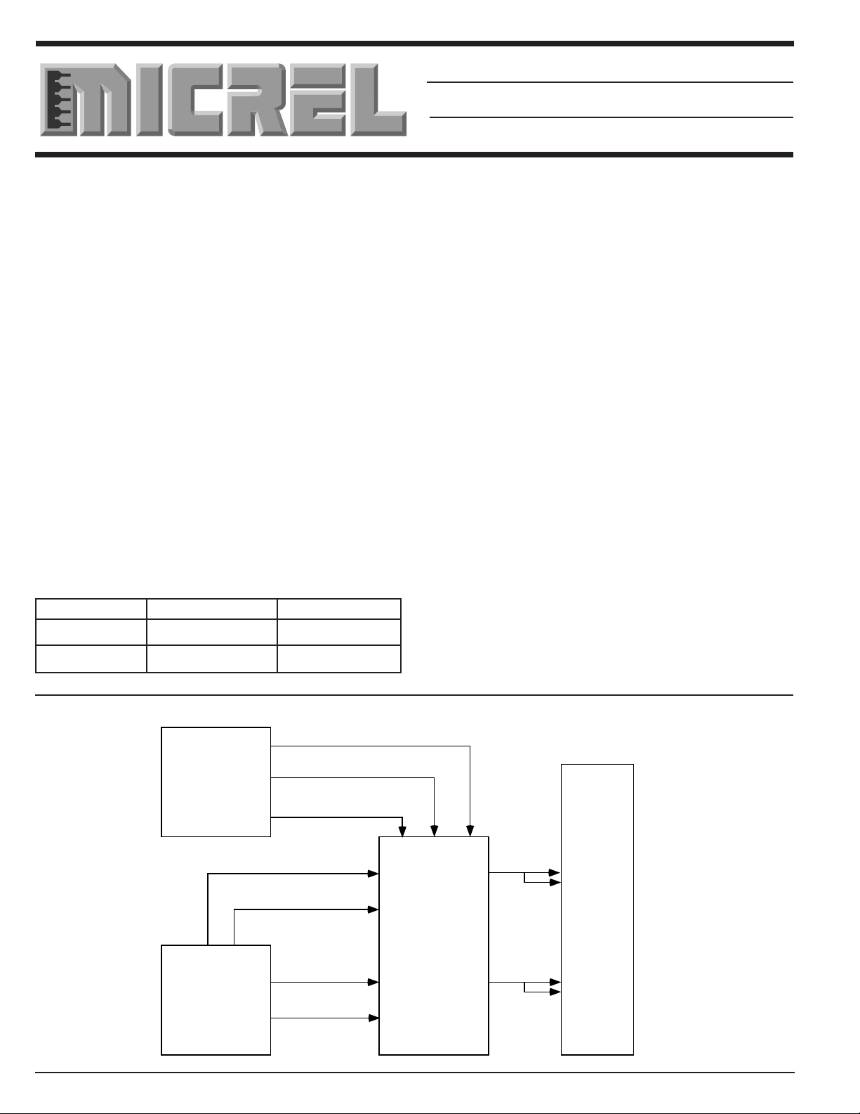
T ypical Application
5V
System
Power
Supply
PCMCIA
Card Slot
Controller
3.3V
12V
V
VPPIN V
CC3
EN0
EN1
MIC2561
V
CC5_EN
V
CC3_EN
IN
IN
CC5
V
V
V
PP1
PP2
CC
PCMCIA
Card Slot
2-30 1997
Page 2
MIC2561 Micrel
Absolute Maximum Ratings (Notes 1 and 2)
Power Dissipation, T
SOIC............................................................ 800 mW
Derating Factors (To Ambient)
SOIC........................................................... 4 mW/°C
Storage Temperature ............................–65°C to +150°C
Maximum Operating Temperature (Die) ................ 125°C
Operating Temperature (Ambient) ..............0°C to +70°C
Lead Temperature (5 sec)...................................... 260°C
AMBIENT
≤ 25°C ....
Internally Limited
Supply Voltage, V
V
IN ....................................................... V
CC3
V
IN ............................................................. 7.5V
CC5
Logic Input Voltages.................................. –0.3V to +15V
Output Current (each Output)
V
PP OUT
V
CC OUT
V
CC OUT
..............................................
............................................
, Suspend Mode.............................. 600mA
...................................................
PP IN
Internally Limited
Internally Limited
CC5
15V
IN
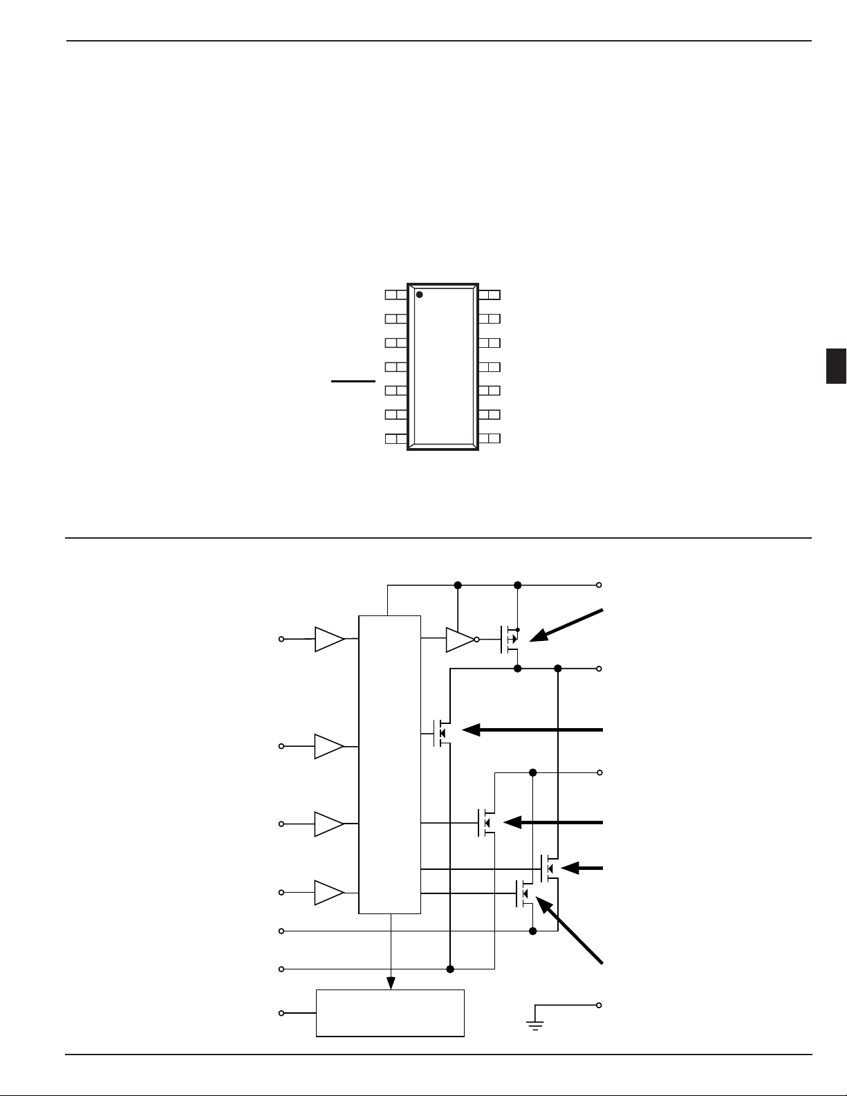
Pin Configuration
Note: Both V
Logic Block Diagram
V
CC5_EN
V
CC3_EN
EN0
EN1
FLAG
VPP IN
VPP OUT
14-Pin SO Package
IN pins must be connected. All three V
CC3
EN1
14
13
2
12
3
11
4
10
5
6
7
9
8
GND
V
CC3
V
CC
V
CC3
V
CC
V
CC5
V
CC
CC
IN
OUT
IN
OUT
IN
OUT
OUT pins must be connected.
V
IN
PP
550mΩ
V
PP OUT
2
MIC2561
Control
EN0
V
CC5_EN
V
CC3_EN
V
IN
CC3
V
IN
CC5
Flag
1997 2-31
I
Limit
Logic
/ Thermal Shut Down
700mΩ
V
CC OUT
210mΩ
2Ω
110mΩ
GND
Page 3

MIC2561 Micrel
Electrical Characteristics:
(Over operating temperature range with V
CC3
IN = 3.3V, V
IN = 5.0V, VPP IN = 12V unless
CC5
otherwise specified.)
Symbol Parameter Conditions Min Typ Max Units
INPUT
V
IH
V
IL
I
IN
Logic 1 Input Voltage 2.2 15 V
Logic 0 Input Voltage –0.3 0.8 V
Input Current 0 V < VIN < 5.5V ±1 µA
VPP OUTPUT
I
PP OUT
Hi-Z Leakage Current 0 ≤ V
I
PPSC
R
O
High Impedance Output Shutdown Mode 0.1 50 µA
PP OUT
Short Circuit Current Limit V
PP OUT
Switch Resistance, Select V
I
PP OUT
= –1000mA (Sourcing) Select V
Select V
≤ 12V
= 0 0.2 A
PP OUT
PP OUT
PP OUT
= 12V 0.55 1 Ω
= 5V 0.7 1
= 3.3V 2 3
R
O
Switch Resistance, Select V
I
PP OUT
= 50µA (Sinking)
VPP SWITCHING TIME (See Figure 1)
t
1
t
2
t
3
t
4
t
5
t
6
Output Turn-On Rise Time V
Output Turn-On Rise Time V
Output Turn-On Rise Time V
Output Rise Time V
Output Turn-Off Delay V
Output Turn-Off Delay V
VCC OUTPUT
I
CC OUT
High Impedance Output 1 ≤ V
Hi-Z Leakage Current
PP OUT
PP OUT
PP OUT
PP OUT
PP OUT
PP OUT
PP OUT
CC OUT
= Clamped to Ground 0.75 2 kΩ
= Hi-Z to 5V 50 µs
= Hi-Z to 3.3V 40 µs
= Hi-Z to 12V 300 µs
= 3.3V or 5V to 12V 30 µs
= 12V to 3.3V or 5V 25 75 µs
= 5V to Hi-Z 75 200 ns
≤ 5V 0.1 10 µA
I
CCSC
R
O
R
O
Short Circuit Current Limit V
Switch Resistance, I
V
CC OUT
= 5.0V
Switch Resistance, I
V
CC OUT
= 3.3V
CC OUT
CC OUT
CC OUT
= 0 1.5 2 A
= –650 mA (Sourcing) 210 300 mΩ
= –650 mA (Sourcing) 110 185 mΩ
2-32 1997
Page 4

MIC2561 Micrel
Electrical Characteristics (continued)
Symbol Parameter Conditions Min Typ Max Units
VCC SWITCHING TIME
t
1
t
2
t
3
t
4
Rise Time (10% to 90%) V
Rise Time (10% to 90%) V
Fall Time (note 3) V
Rise Time V
POWER SUPPLY
I
CC5
I
CC3
I
IN V
PP
V
CC5
V
CC3
PP
I
PP OUT
= 0V to 3.3V, I
= 0V to 5.0V 50 60 µs
= 5.0V to 0V or 3.3V to 0V 40 µs
= Hi-Z to 5V 60 µs
= 0 0.01 10 µA
= 5V or 3.3V, I
= Hi-Z (Sleep Mode) 0.01 10
IN Supply Current I
IN Supply Current V
CC OUT
CC OUT
CC OUT
CC OUT
CC OUT
CC OUT
V
CC OUT
IN Supply Current VCC Active, V
=0
V
PP OUT
= HiZ, 0, or V
PP OUT
= 750mA 70 140 µs
OUT
CC OUT
= 0 30 100 µA
= 5V or 3.3V 15 30 µA
PP
0.01 10
2
V
IN Operating Input Voltage V
CC5
V
IN Operating Input Voltage V
CC3
V
PP IN
Operating Input Voltage 8.0 12.0 14.5 V
CC5
CC3
IN ≥ V
IN ≤ V
IN V
CC3
IN 2.8 3.3 V
CC5
IN 5.0 6 V
CC3
IN V
CC5
SUSPEND MODE (NOTE 6)
I
CC3
RON V
CC
NOTE 1: Functional operation above the absolute maximum stress ratings is not implied.
NOTE 2: Static-sensitive device. Store only in conductive containers. Handling personnel and equipment should be grounded to prevent damage
NOTE 3: From 90% of V
NOTE 6: Suspend mode is a pseudo power-down mode the MIC2561 automatically allows when V
Suspend Mode Active Current V
(from V
V
CC OUT RON
from static discharge.
OUT = 3.3V is selected. Under these conditions, the MIC2561 functions in a reduced capacity mode where VCC output of 3.3V is allowed,
but at lower current levels (higher switch ON resistance).
)V
CC3
to 10% of V
OUT
. RL = 2.1kΩ
OUT
= 0V, V
PP IN
= Enabled
CC5
= Disabled (Hi-Z or 0V)
V
PP
V
= 0V, V
PP IN
V
= Enabled
CC3
= Disabled (Hi-Z or 0V)
V
PP
CC5
CC5
= V
= V
= 3.3V 30 100 µA
CC3
= 3.3V 4.5 6 Ω
CC3
= 0V, VPP OUT is deselected, and V
PP IN
CC
1997 2-33
Page 5
MIC2561 Micrel
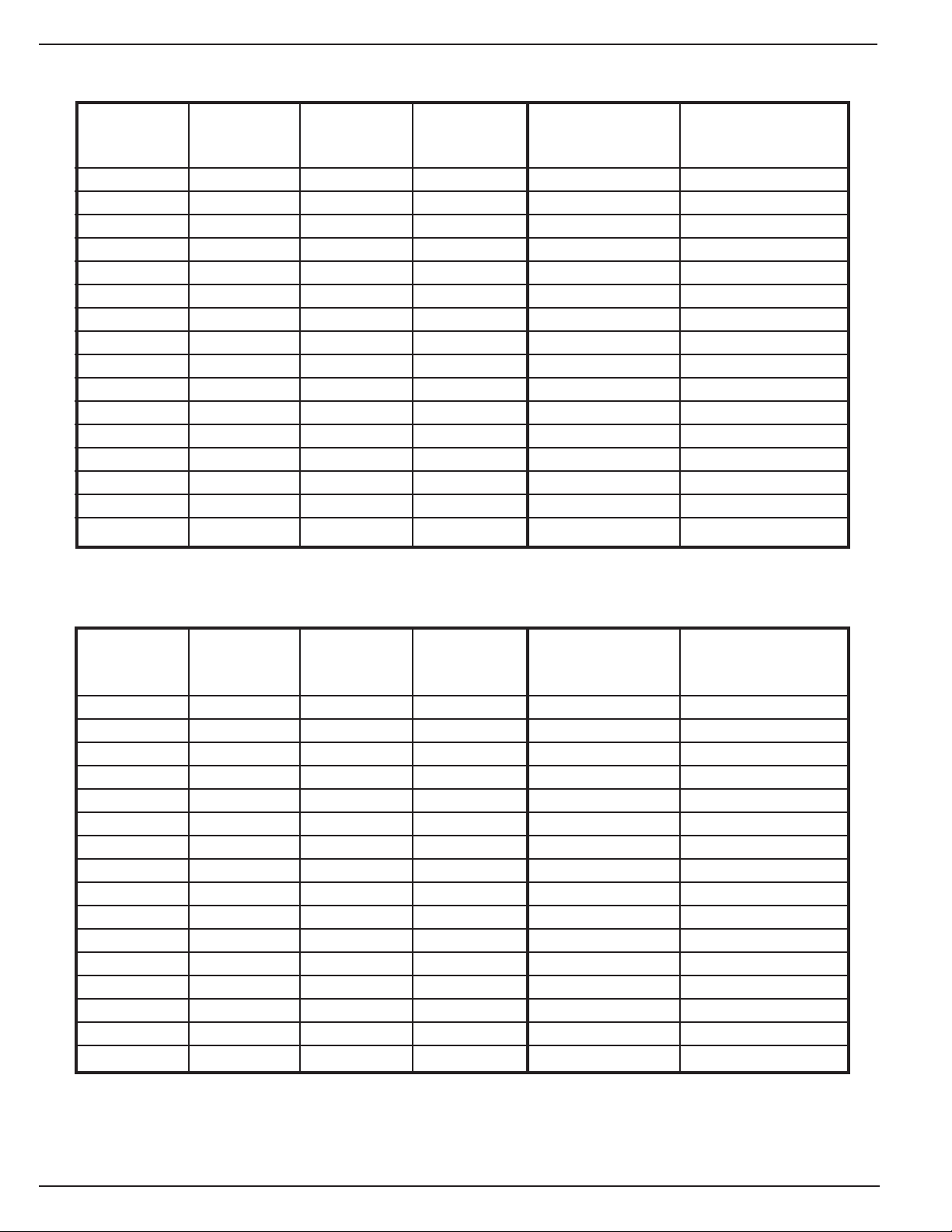
MIC2561-0 Control Logic Table
Pin 1 Pin 2 Pin 4 Pin 3 Pins 8 & 12 Pin 7
V
CC5_EN
0000 High Z High Z
0001 High Z High Z
0010 High Z High Z
0011 High Z Clamped to Ground
0100 3.3 High Z
0101 3.3 3.3
0110 3.3 12
0111 3.3Clamped to Ground
1000 5 High Z
1001 5 5
1010 5 12
1011 5Clamped to Ground
1100 3.3 High Z
1101 3.3 3.3
1110 3.3 5
1111 3.3Clamped to Ground
V
CC3_EN
EN1 EN0 V
CC OUT
V
PP OUT
MIC2561-1 Logic (Compatible with Cirrus Logic CL-PD6710 & CL-PD6720 Controllers)
Pin 1 Pin 2 Pin 4 Pin 3 Pins 8 & 12 Pin 7
V
CC5_EN
0000 High Z Clamped to Ground
0001 High Z High Z
0010 High Z High Z
0011 High Z High Z
0100 5Clamped to Ground
0101 5 5
0110 5 12
0111 5 High Z
1000 3.3Clamped to Ground
1001 3.3 3.3
1010 3.3 12
1011 3.3 High Z
1100 High Z Clamped to Ground
1101 High Z High Z
1110 High Z High Z
1111 High Z High Z
V
CC3_EN
V
PP_PGM
V
PP_VCC
V
CC OUT
V
PP OUT
Note: other control logic patterns are available. Please contact Micrel for details.
2-34 1997
Page 6
MIC2561 Micrel
Applications Information
PCMCIA VCC and VPP control is easily accomplished using
the MIC2561 voltage selector/switch IC. Four control bits
determine V
CC OUT
operate mode condition. V
(3.3V or 5V), VPP, or a high impedance state are available.
When the VCC high impedance condition is selected, the
device switches into “sleep” mode and draws only nanoamperes of leakage current. An error flag falls low if the output
is improper, because of overtemperature or overcurrent
faults. Full protection from hot switching is provided which
prevents feedback from the V
12V to 5V, for example) by locking out the low voltage switch
until V
PP OUT
drops below VCC. The VCC output is similarly
protected against 5V to 3.3V shoot through.
The MIC2561 is a low-resistance power MOSFET switching
matrix that operates from the computer system main power
supply. Device logic power is obtained from V
internal MOSFET drive is obtained from the VPP IN pin
(usually +12V) during normal operation. If +12V is not available, the MIC2561 automatically switches into “suspend”
mode, where V
CC OUT
switch resistance. Internal break-before-make switches determine the output voltage and device mode.
and V
PP OUT
PP OUT
PP OUT
voltage and standby/
output voltages of V
to the VCC inputs (from
and
CC3
CC
can be switched to 3.3V, but at higher
Supply Bypassing
External capacitors are not required for operation. The
MIC2561 is a switch and has no stability problems. For best
results however, bypass V
CC3
IN, V
CC5
IN, and V
PP
IN
inputs with filter capacitors to improve output ripple. As all
internal device logic and voltage/current comparison functions are powered from the V
IN line, supply bypass of this
CC3
line is the most critical, and may be necessary in some cases.
In the most stubborn layouts, up to 0.47µF may be necessary.
Both V
CC OUT
and V
PP OUT
pins may have 0.01µF to 0.1µF
capacitors for noise reduction and electrostatic discharge
(ESD) damage prevention. Larger values of output capacitor
might create current spikes during transitions, requiring larger
bypass capacitors on the V
CC3
IN, V
CC5
IN, and V
PP
IN pins.
PCMCIA Implementation
The Personal Computer Memory Card International Association (PCMCIA) specification requires two VPP supply pins per
PCMCIA slot. VPP is primarily used for programming Flash
(EEPROM) memory cards. The two VPP supply pins may be
programmed to different voltages. Fully implementing PCMCIA specifications requires a MIC2561, a MIC2557 PCMCIA
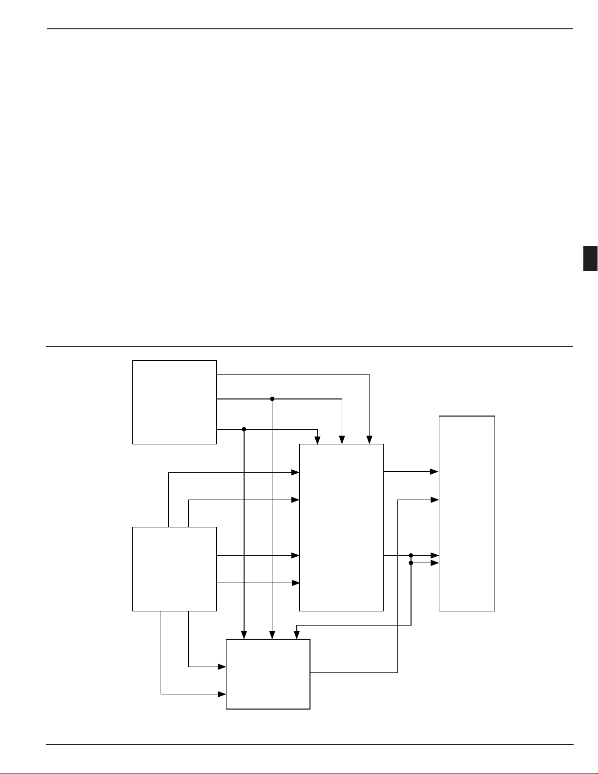
VPP Switching Matrix, and a controller. Figure 3 shows this
full configuration, supporting both 5.0V and 3.3V VCC operation.
2
System
Power
Supply
PCMCIA
Card Slot
Controller
5V
3.3V
12V
V
PP IN
PCMCIA
VPPIN V
CC3
EN0
EN1
MIC2561
V
CC5_EN
V
CC3_EN
V
V
CC
DD
INV
IN
CC5
V
V
V
PP1
PP2
CC
Card Slot
EN0
EN1
V
PP
MIC2557
OUT
Figure 3. MIC2561 Typical PCMCIA memory card application with dual VCC (5.0V or 3.3V) and separate V
1997 2-35
PP1
and V
PP2.
Page 7
MIC2561 Micrel
5V
System
Power
Supply
PCMCIA
Card Slot
Controller
3.3V
12V
V
VPPIN V
CC3
EN0
EN1
MIC2561
V
CC5_EN
V
CC3_EN
IN
IN
CC5
V
V
V
PP1
PP2
CC
PCMCIA
Card Slot
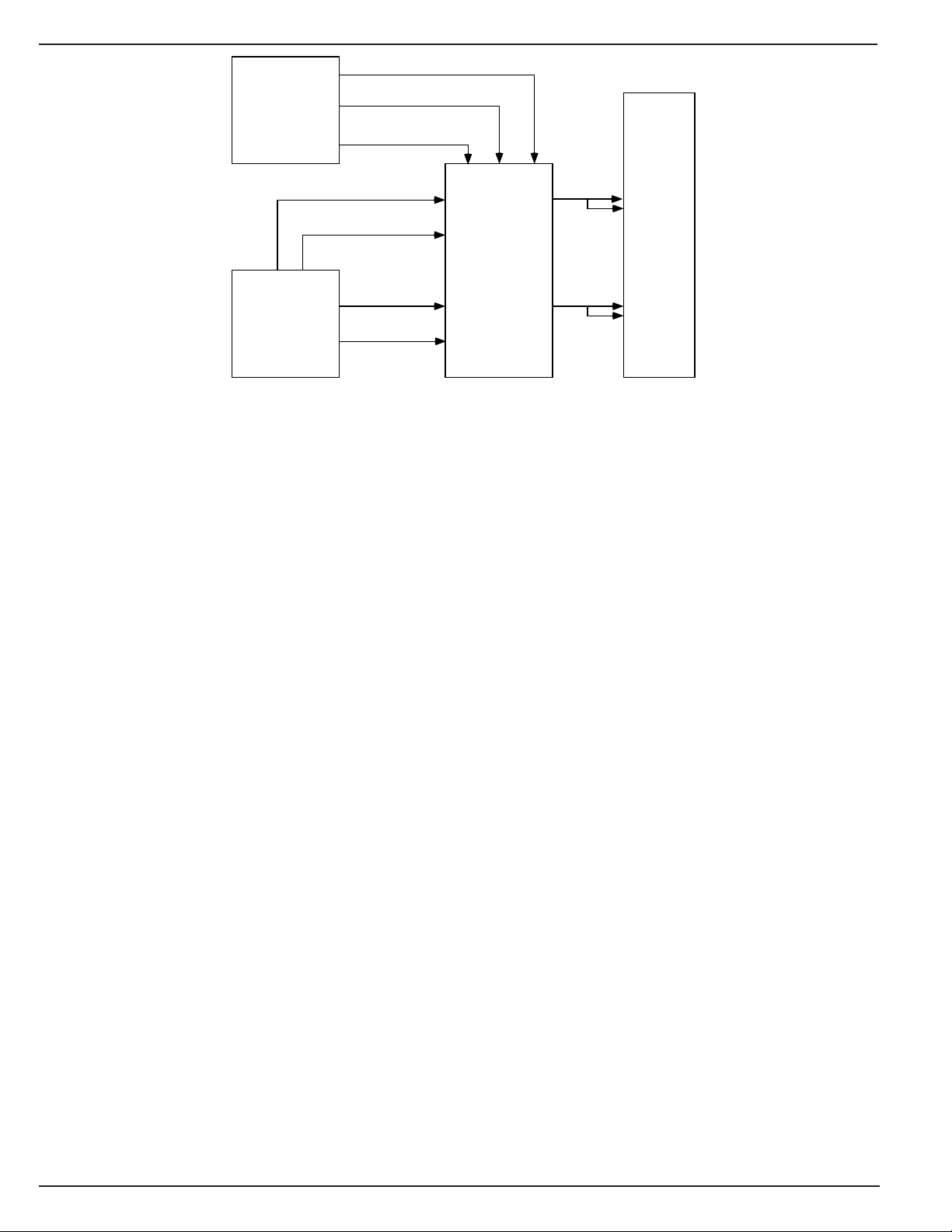
Figure 4. MIC2561 Typical PCMCIA memory card application with dual VCC (5.0V or 3.3V). Note that V
driven together.
However, many cost sensitive designs (especially notebook/
palmtop computers) connect V
PP1
to V
and the MIC2557
PP2
is not required. This circuit is shown in Figure 4.
When a memory card is initially inserted, it should receive
VCC — either 3.3V ± 0.3V or 5.0V ±5%. The initial voltage is
determined by a combination of mechanical socket “keys”
and voltage sense pins. The card sends a handshaking data
stream to the controller, which then determines whether or
not this card requires VPP and if the card is designed for dual
VCC. If the card is compatible with and desires a different V
level, the controller commands this change by disabling VCC,
waiting at least 100ms, and then re-enabling the other V
voltage.
CC
CC
level selected. The lockout delay time varies with the load
current and the capacitor on V
and nominal I
PP OUT
, the delay is approximately 250µs.
PP OUT
. With a 0.1µF capacitor
Internal drive and bias voltage is derived from V
device control logic is powered from V
CC3
threshold voltages are compatible with common PCMCIA
controllers using either 3.3V or 5V supplies. No pull-up
resistors are required at the control inputs of the MIC2561.
Output Current and Protection
MIC2561 output switches are capable of more current than
needed in PCMCIA applications and meet or exceed all
PCMCIA specifications. For system and card protection,
output currents are internally limited. For full system protec-
If no card is inserted or the system is in sleep mode, the
controller outputs a (V
MIC2561, which shuts down VCC. This also places the switch
CC3
IN, V
IN) = (0,0) to the
CC5
into a high impedance output shutdown (sleep) mode, where
current consumption drops to nearly zero, with only tiny
CMOS leakage currents flowing.
During Flash memory programming with standard (+12V)
Flash memories, the PCMCIA controller outputs a (1,0) to the
EN0, EN1 control pins of the MIC2561, which connects
VPPIN to V
PP OUT
. The low ON resistance of the MIC2561
switches allow using small bypass capacitors (in some cases,
none at all) on the V
CC OUT
and V
PP OUT
pins, with the main
filtering action performed by a large filter capacitor on the
input supply voltage to VPPIN (usually the main power
supply filter capacitor is sufficient). The V
PP OUT
transition
from VCC to 12.0V typically takes 15µs. After programming is
completed, the controller outputs a (EN1, EN0) = (0,1) to the
MIC2561, which then reduces V
PP OUT
to the VCC level for
read verification. Break-before-make switching action reduces switching transients and lowers maximum current
spikes through the switch from the output capacitor. The flag
comparator prevents having high voltage on the VPP
OUT
capacitor from contaminating the VCC inputs, by disabling the
low voltage VPP switches until VPP
drops below the V
OUT
CC
tion, long term (millisecond or longer) output short circuits
invoke overtemperature shutdown, protecting the MIC2561,
the system power supplies, the card socket pins, and the
memory card. The MIC2561 overtemperature shutdown occurs at a die temperature of 110°C.
Suspend Mode
An additional feature in the MIC2561 is a pseudo power-down
mode, Suspend Mode, which allows operation without a V
IN supply. In Suspend Mode, the MIC2561 supplies 3.3V to
VCC OUT whenever a VCC output of 3.3V is enabled by the
PCMCIA controller. This mode allows the system designer
the ability to turn OFF the VPP supply generator to save
power when it is not specifically required. The PCMCIA card
receives VCC at reduced capacity during Suspend Mode, as
the switch resistance rises to approximately 4.5Ω.
High Current VCC Operation Without a
+12V Supply
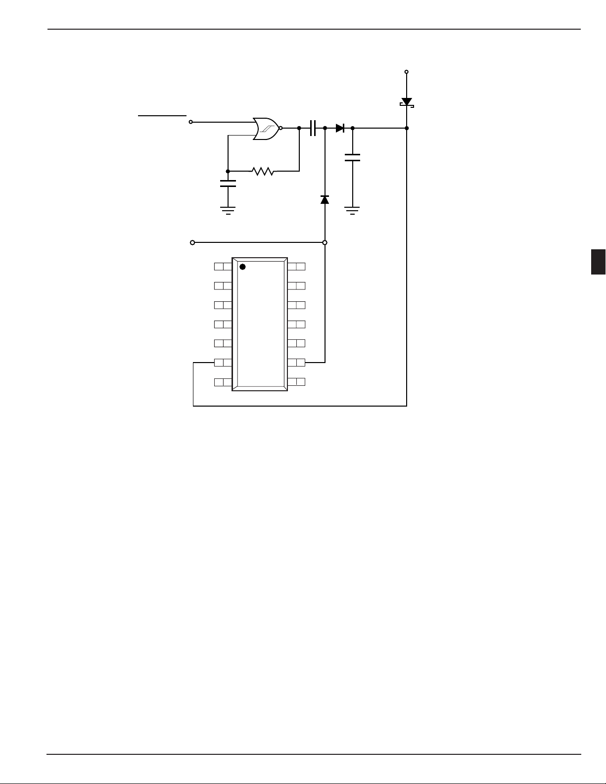
Figure 5 shows the MIC2561 with VCC switch bias provided
by a simple charge pump. This enables the system designer
to achieve full VCC performance without a +12V supply,
which is often helpful in battery powered systems that only
provide +12V when it is needed. These on-demand +12V
PP1
and V
PP
are
PP2
IN. Internal
IN. Input logic
PP
2-36 1997
Page 8
MIC2561 Micrel
Drive Enable
+5V
4.7kΩ
0.01µF
2
3
4
5
14
13
12
11
10
1N914
Switched V
1N9140.1µF
0.02µF
PP IN
(Optional Schottky)
2
6
7
9
8
Figure 5. Circuit for generating bias drive for the VCC switches when +12V is not readily available.
supplies generally have a quiescent current draw of a few
milliamperes, which is far more than the microamperes used
by the MIC2561. The charge pump of Figure 5 provides this
low current, using about 100µA when enabled. When V
= 12V is selected, however, the on-demand VPP generator
PP OUT
must be used, as this charge pump cannot deliver the current
required for Flash memory programming. The Schottky diode
may not be necessary, depending on the configuration of the
on-demand +12V generator and whether any other loads are
on this line.
1997 2-37
 Loading...