

Page 1
MIC2529 Micrel
MIC2529
Single-Channel USB Power Controller
Advance Information
General Description
The MIC2529 is a high-side power switch optimized for selfpowered (individual port switching) and bus-powered (ganged
port switching) Universal Serial Bus (USB) hub applications.
An on-board voltage regulator provides the 3.3V supply
voltage needed for many USB microcontrollers reducing
board component count.
The MIC2529 satisfies the following USB requirements: it
supplies up to 500mA as required by USB downstream
devices; the switch’s low on-resistance meets USB voltage
drop requirements; fault current is limited to typically 750mA,
well below the UL 25VA safety requirement; and a flag output
is available to indicate fault conditions to the local USB
controller. Soft start eliminates the momentary voltage drop
on the upstream port that may occur when the switch is
enabled in bus-powered applications.
A low-dropout (LDO) regulator provides 3.3V at loads up to
100mA and includes an enable pin for low current shutdown.
Both enable inputs are compatible with 3.3V and 5V logic.
Thermal shutdown prevents catastrophic failure from highcurrent loads.
The MIC2529 is available in an 8-pin SOIC package with
active-high or active-low enable circuitry on switch.
Features
• Compliant to USB specifications
• UL Recognized Component
• On-board 3.3V, 100mA low-dropout regulator
• 500mA minimum continuous switch load current
• 160mΩ maximum on-resistance
• 750mA typical current limit
• Open-drain fault flag pin for switch
• Output can be forced higher than input (off-state)
• Thermal shutdown
• 1ms turn-on (soft-start) and fast turnoff
• Available with active-high or active-low switch enable
• Active-high enable on 3.3V regulated output
• 8-pin SOIC package
Applications
• USB self-powered hubs
• USB bus-powered hubs
• USB keyboard hubs
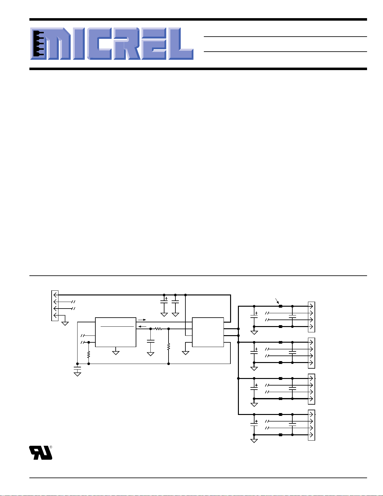
Typical Applications
Upstream V
D+
D–
GND
BUS
3.3V USB Controller
V+
OVERCURRENT
D–
D+
1.5k*
5%
1µF
* Speed sense termination resistor. Must be connected
between V
†
33µF tantalum or 100µF electrolytics are recommended.
4.40V to 5.25V
4.7
µF
ON/OFF
GND
Bold lines indicate
0.1" wide, 1-oz. copper
high-current traces.
and D+ to indicate high speed operation.
3VOUT
10k
0.1µF
10k
0.1
µF
MIC2529
83
EN IN
12
FLG OUT
67
3VEN
54
GND
OUT
3VOUT
33µF
33µF
33µF
33µF
Ferrite
Bead
V
BUS
†
0.01µF
†
0.01µF
†
0.01µF
†
0.01µF
D+
D–
GND
V
BUS
D+
D–
GND
V
BUS
D+
D–
GND
V
BUS
D+
D–
GND
Downstream
USB
Port 1
100mA max.
Downstream
USB
Port 2
100mA max.
Downstream
USB
Port 3
100mA max.
Downstream
USB
Port 4
100mA max.
4-Port Ganged Bus-Powered Hub
UL Recognized Component
June 1999 1 MIC2529
Page 2
MIC2529 Micrel
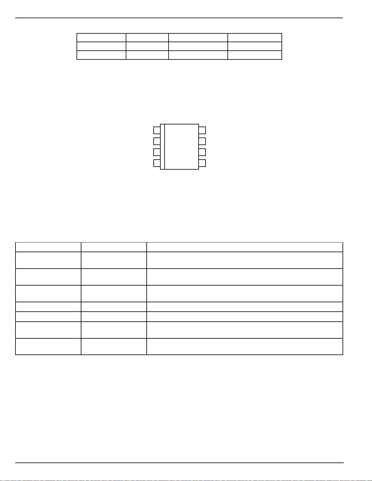
Ordering Information
Part Number Switch Enable Temperature Range Package
MIC2529-1BM Active High –40°C to +85°C 8-Pin SOIC
MIC2529-2BM Active Low –40°C to +85°C 8-Pin SOIC
Pin Configuration
MIC2529
FLG
1
EN
8
OUT
3VOUT
Pin Description
Pin Number Pin Name Pin Function
1 FLG Fault Flag (Output): Active-low, open-drain output. Indicates overcurrent and
2, 7 OUT Switch Output: Output MOSFET source. Typically connected to switched
3 IN Supply Voltage Input. Supply to switch and regulator. Connect to positive
4 3VOUT 3.3V Regulator Output
5 GND Ground: Supply return.
6 3VEN Regulator Enable (Input): Logic-compatible input. Logic high = enable, logic
8 EN Switch Enable (Input): Logic-compatible enable input. High input = 2.1V
7
6
5
OUT
3VEN
GND
IN
2
3
4
8-Pin SOIC (M)
thermal shutdown switch conditions.
side of load. Pin 2 and 7 must be connected together externally.
supply.
low or open = shutdown. Do not float.
typical. Low input = 1.9V typical. (-1 active high, -2 active low) Do not float.
MIC2529 2 June 1999
Page 3
MIC2529 Micrel
Absolute Maximum Ratings (Note 1)
Supply Voltage (VIN) .....................................................+6V
Fault Flag Voltage (V
Fault Flag Current (I
Switch Output Voltage (OUT)........................................+6V
Switch Output Current (I
)..............................................+6V
FLG
) ............................................50mA
FLG
) ...................Internally Limited
OUT
Operating Ratings (Note 2)
Supply Voltage (VIN) ...................................... +3V to +5.5V
Ambient Temperature (TA).........................–40°C to +85°C
Thermal Resistance
SOIC (θJA).........................................................160°C/W
Switch Control Input (VEN) ........................... –0.3V to +12V
Regulator Control Input (V
).................... –20V to +20V
3VEN
Storage Temperature (TS) ....................... –65°C to +150°C
Lead Temperature (soldering 5 sec.) ........................ 260°C
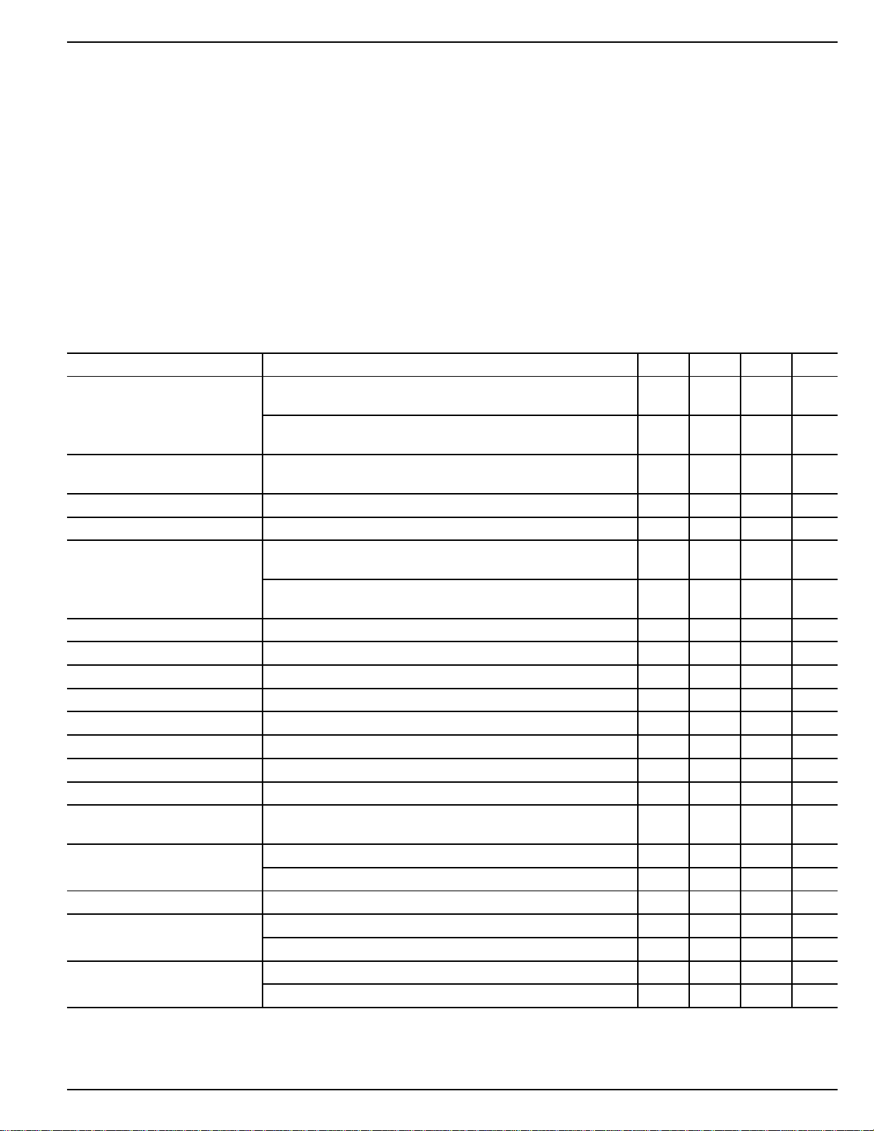
Electrical Characteristics
VIN = +5V; TA = 25°C; unless noted.
Parameter Condition Min Typ Max Units
Supply Current V
EN Input Threshold low to high transition 2.1 2.4 V
Enable Input Current VEN = 0 - 5.5V 0.01 µA
Enable Input Capacitance 1pF
Switch Resistance V
= high, switch EN off, Note 3 80 150 µA
3VEN
V
= high, switch EN on, OUT = open, Note 3 160 300 µA
3VEN
high to low transition, Note 3 0.8 1.9 V
= 5V; I
IN
= 500mA 120 mΩ
OUT
VIN = 3.3V; I
Output Turn-On Delay RL = 10Ω 0.25 ms
Output Turn-On Rise Time RL = 10Ω 3ms
Output Turnoff Delay RL = 10Ω 120µs
Output Turnoff Fall Time RL = 10Ω 120µs
Output Leakage Current 10 µA
Continuous Load Current FLG not active 0.5 A
Short Circuit Current Limit enabled into load, V
Current-Limit Threshold ramped load applied to enabled output, V
Overtemperature Shutdown T
Threshold TJ decreasing 125 °C
Error Flag Output Resistance VIN = 5V, IL = 10mA 20 Ω
Error-Flag Off Current V
3VEN Input Threshold enable input logic-low voltage (regulator shutdown) 0.4 V
3VEN Input Current VIL ≤ 0.4V 0.01 –1 µA
increasing 135 °C
J
VIN = 3.3V, IL = 10mA 30 Ω
= 5V 0.01 1 µA
FLAG
enable input logic-high voltage (regulator enabled) 2.0 V
VIH ≥ 2.0V 5 20 µA
= 500mA 160 mΩ
OUT
= 0V 0.5 0.75 1.25 A
OUT
= 0V, Note 4 0.95 1.50 A
OUT
June 1999 3 MIC2529
Page 4
MIC2529 Micrel
Parameter Condition Min Typ Max Units
Regulator Output Voltage VIN = 4.0V to 5.25V, IL = 100mA 3.14 3.3 3.47 V
Regulator Output Voltage Note 5 50 ppm/°C
Temperature Coefficient
Regulator Line Regulation VIN = 4.0V to 5.25V 0.3 mV
Regulator Load Regulation IL = 0.1mA to 100mA 3 mV
Regulator Dropout Voltage IL = 100mA, Note 6 mV
Regulator Current Limit 3V
Note 1. Exceeding the absolute maximum rating may damage the device. Devices are ESD sensitive. Handling precautions recommended.
Note 2. The device is not guaranteed to function outside its operating rating.
Note 3. Off is ≤ 0.8V and on is ≥ 2.4V for the MIC2529-1 switch. Off is ≥ 2.4V and on is ≤ 0.8V for the MIC2529-2 switch. The enable input has
approximately 200mV of hysteresis. See control threshold charts. Limits do not include 3VOUT load current of 100µA during test.
Note 4. See “Functional Characteristics: Current-Limit Response” photo.
Note 5. Output voltage temperature coefficient is defined as the worst case voltage change divided by the total temperature range.
Note 6. Dropout voltage is defined as the input to output differential at which the output voltage drops 2% below its nominal value measured at 1V
differential.
= 0V 320 mA
OUT
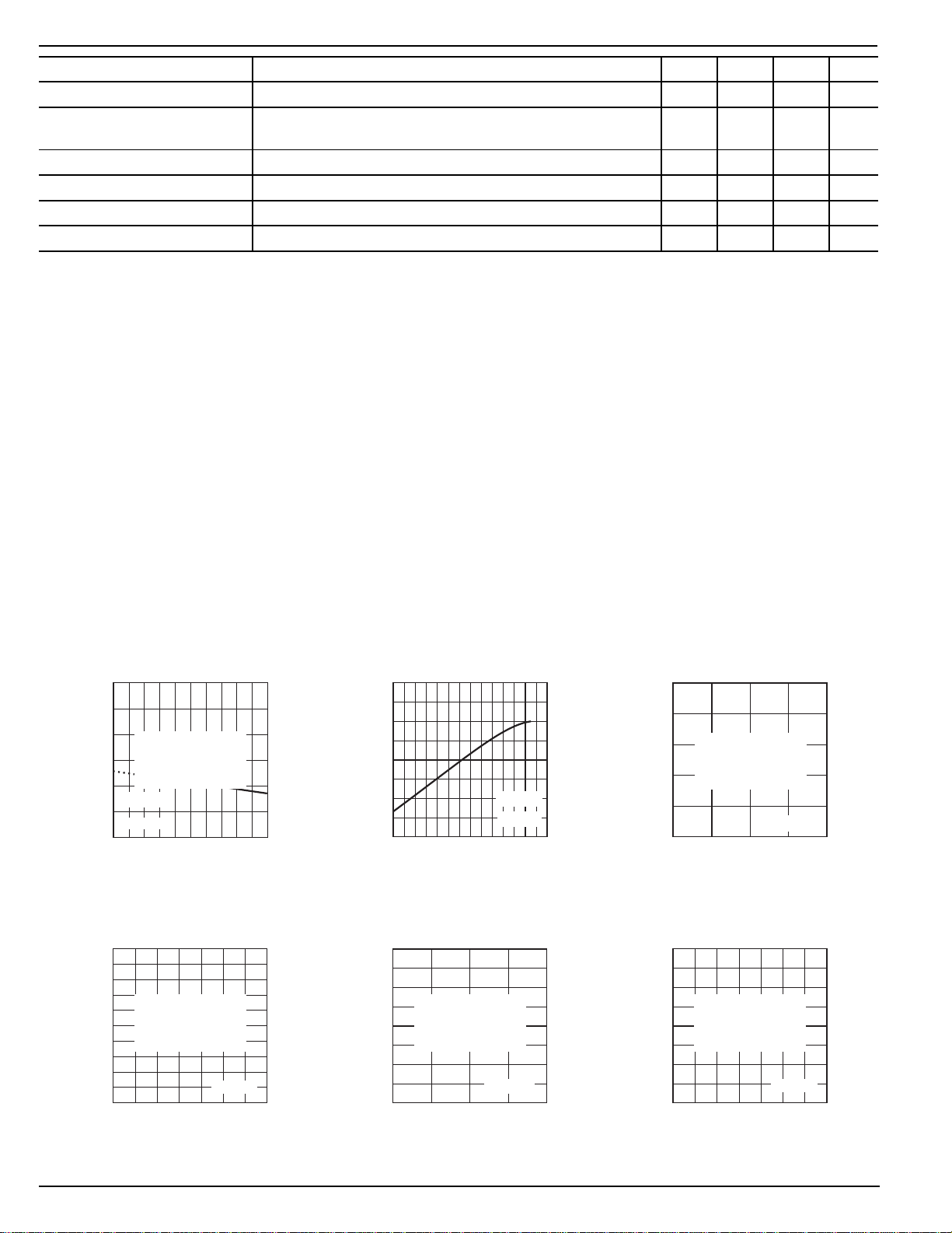
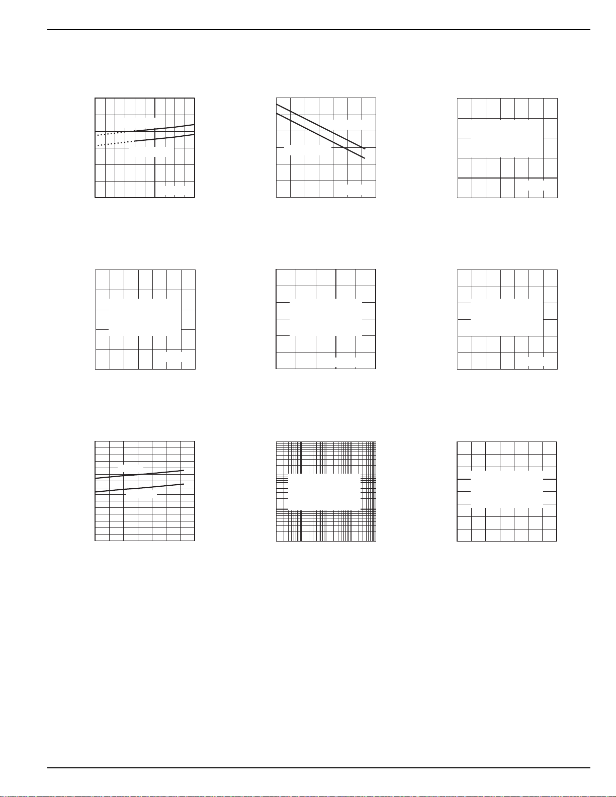
Typical Characteristics
Output On-Resistance
vs. Supply Voltage
140
120
100
OUTPUT RESISTANCE (mΩ)
200
180
160
140
120
100
SUPPLY CURRENT (µA)
Awaiting Further
Characterization
Data
RL = 44Ω
T = 25°C
80
3.0 3.5 4.0 4.5 5.0 5.5
SUPPLY VOLTAGE (V)
On-State Supply Current
vs. Temperature
Awaiting Further
Characterization
80
60
40
20
0
-40 -20 0 20 40 60 80 100
Data
VIN = 5V
TEMPERATURE (°C)
Output On-Resistance
140
120
100
ON-RESISTANCE (mΩ)
vs. Temperature
80
60
-40 -20 0 20 40 60 80 100
TEMPERATURE (°C)
RL = 44Ω
VIN = 5V
Off-State Supply Current
vs. Supply Voltage
2.0
1.5
Awaiting Further
1.0
0.5
SUPPLY CURRENT (µA)
Characterization
Data
TA = 25°C
0
23456
SUPPLY VOLTAGE (V)
On-State Supply Current
vs. Supply Voltage
200
160
120
Awaiting Further
Characterization
80
40
SUPPLY CURRENT (µA)
0
23456
Data
TA = 25°C
SUPPLY VOLTAGE (V)
Off-State Supply Current
2.0
1.5
vs. Temperature
Awaiting Further
1.0
0.5
SUPPLY CURRENT (µA)
Characterization
Data
VIN = 5V
0
-40 -20 0 20 40 60 80 100
TEMPERATURE (°C)
MIC2529 4 June 1999
Page 5
MIC2529 Micrel
0
1
2
3
-40 -20 0 20 40 60 80 100
SWITCH OUTPUT (A)
TEMPERATURE (°C)
Short Circuit Output Current
vs. Temperature
VIN = 5V
0
50
100
150
200
250
300
350
400
-40 -20 0 20 40 60 80 100
DROPOUT VOLTAGE (V)
TEMPERATURE (°C)
Regulator Dropout Voltage
vs. Temperature
0
1
2
3
4
5
-40 -20 0 20 40 60 80 100
TIME (ms)
TEMPERATURE (°C)
Output Rise Time
vs. Temperature
VIN = 5V
Switch Enable Threshold
vs. Supply Voltage
2.5
2.0
1.5
SWITCH ENABLE VOLTAGE (V)
1.0
VEN RISING
VEN FALLING
TA = 25°C
3.0 3.5 4.0 4.5 5.0 5.5
SUPPLY VOLTAGE (V)
Output Fall Time
vs. Temperature
50
40
Awaiting Further
30
Characterization
20
TIME (µs)
10
0
-40 -20 0 20 40 60 80 100
Data
VIN = 5V
TEMPERATURE (°C)
Switch Enable Threshold
2.5
2.0
1.5
SWITCH ENABLE VOLTAGE (V)
1.0
vs. Temperature
VEN RISING
VEN FALLING
VIN = 5V
-40 -20 0 20 40 60 80 100
TEMPERATURE (°C)
Threshold Trip Current
vs. Supply Voltage
3
2
Awaiting Further
Characterization
Data
1
SWITCH OUTPUT (A)
0
012345
SUPPLY VOLTAGE (V)
TA = 25°C
Awaiting Further
Characterization
Data
Awaiting Further
Characterization
Data
3.0
2.5
2.0
THRESHOLD VOLTAGE (V)
1.5
-40 -20 0 20 40 60 80 100
June 1999 5 MIC2529
UVLO Threshold Voltage
vs. Temperature
RISING
FALLING
TEMPERATURE (°C)
Regulator Dropout Voltage
1000
vs. Output Current
100
Awaiting Further
Characterization
10
DROPOUT VOLTAGE (V)
1
0.01 0.1 1 10 100
Data
OUTPUT CURRENT (mA)
Awaiting Further
Characterization
Data
Page 6
MIC2529 Micrel
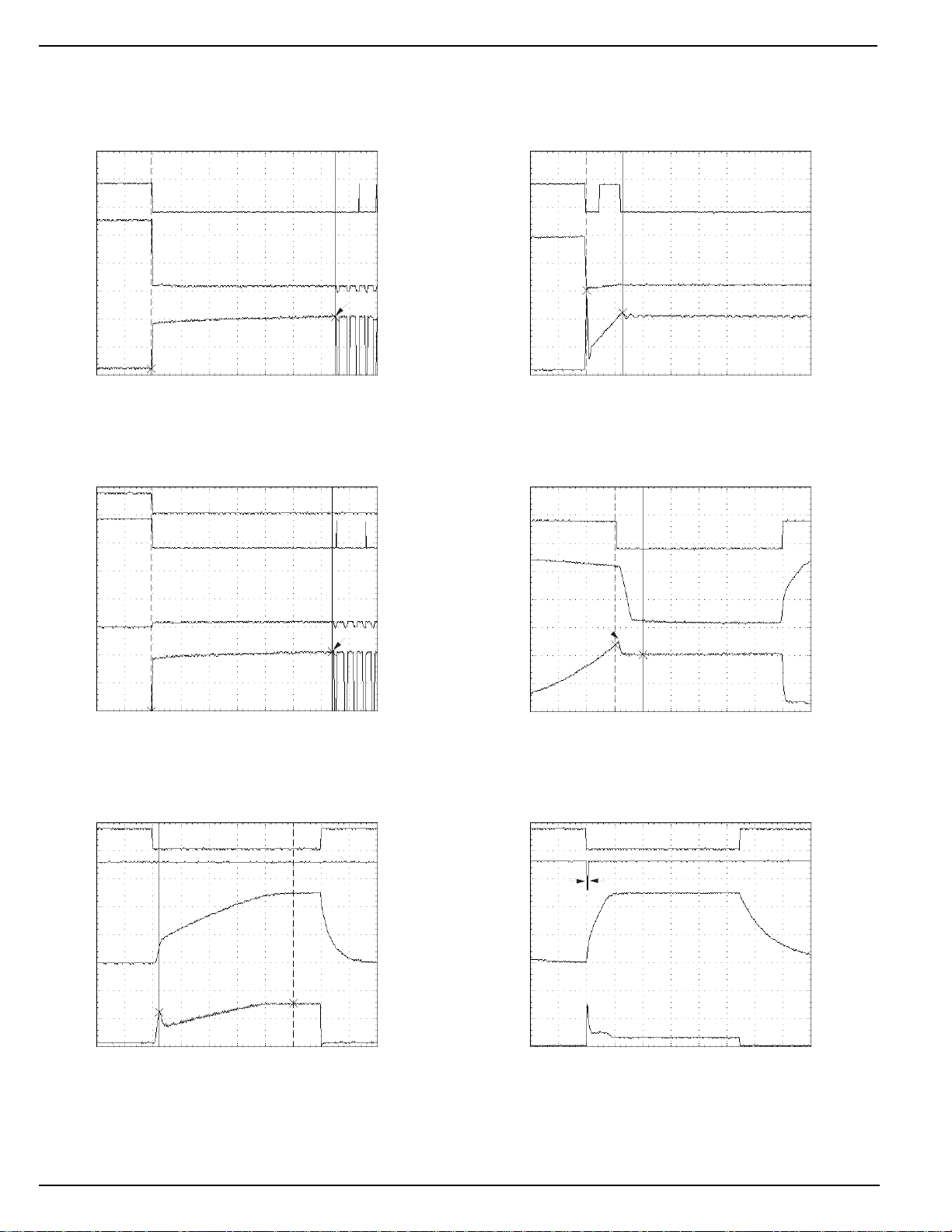
Functional Characteristics
V
V
I
V
V
FLG
OUT
OUT
EN
FLG
Short-Circuit Response
Short Applied to Output
FLG
V
V
(5V/div.)
OUT
(2V/div.)
(5V/div.)
(2V/div.)
Short Circuit Transient Response
Short Applied to Output
Thermal Shutdown
VIN = 5V
= 0.3Ω
R
(500mA/div.)
L
TIME (100ms/div.)
Short Circuit Response
I
OUT
VIN = 5V
(0.5A/div.)
TIME (100µs/div.)
Current Limit Response
Enabled into Short Circuit
(5V/div.)
(5V/div.)
V
FLG
(5V/div.)
V
I
V
V
V
I
OUT
OUT
EN
FLG
OUT
OUT
(2V/div.)
(Regulator Disabled)
= 5V
V
IN
(500mA/div.)
TIME (100ms/div.)
Turn-On and Turnoff
Characteristics
off on off
(5V/div.)
(5V/div.)
(2V/div.)
(100mA/div.)
TIME (1ms/div.)
Thermal Shutdown
VIN = 5V
=40Ω
R
L
= 10µF
C
L
V
I
V
V
V
I
OUT
(2V/div.)
1.24A
Current Limit
Threshold
OUT
(500mA/div.)
TIME (5ms/div.)
Turn-On and Turnoff
Characteristics
EN
off on off
(5V/div.)
FLG
(5V/div.)
OUT
(2V/div.)
OUT
(500mA/div.)
100µs
TIME (5ms/div.)
= 5V
V
IN
= 5V
V
IN
= 40Ω
R
L
= 150µF
C
L
MIC2529 6 June 1999
Page 7
MIC2529 Micrel
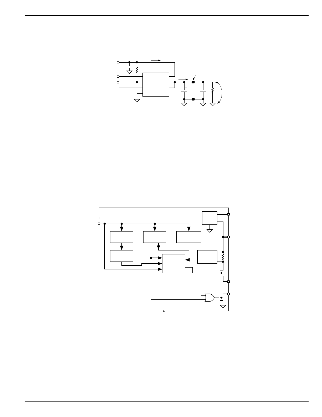
Test Circuit
I
10k
MIC2529
EN IN
FLG OUT
3VEN OUT
GND 3VOUT
IN
Ferrite
Bead
I
OUT
C
0.1µF
L
R
L
V
OUT
5V
0.1µF
V
EN
V
FLG
V
3VEN
Functional Characteristics Test Circuit
Block Diagram
3VEN
EN
CHARGE
MIC2529-x
OSC.
PUMP
THERMAL
SHUTDOWN
GND
REFERENCE
GATE
CONTROL
1.2V
3.3V
LDO
REG
CURRENT
LIMIT
3VOUT
IN
OUT
FLG
June 1999 7 MIC2529
Page 8

MIC2529 Micrel
Functional Description
The MIC2529-1 and MIC2529-2 are high-side power switches
with on-board voltage regulators. Switch fault conditions turn
off or inhibit turn-on of the output transistor, depending upon
the type of fault, and activate the open-drain error flag
transistor, making it sink current to ground.
Input and Output
IN (input) is the power supply connection to the logic circuitry,
drain of the output MOSFET, and the voltage regulator input.
3VOUT is the regulated 3.3V output. OUT (output) is the
source of the MOSFET switch. In a typical circuit current flows
through the switch from IN to OUT toward the load. Both OUT
pins must be connected together externally. If V
than VIN when a switch is disabled, current will flow from OUT
to IN when the switch is enabled since the switch is bidirectional when enabled.
The output MOSFET and driver circuitry are also designed to
allow the MOSFET source to be externally forced to a higher
voltage than the drain (V
> VIN) when the output is off.
OUT
Thermal Shutdown
Thermal shutdown shuts off the switch and activates the flag
if the die temperature exceeds 135°C. 10°C of hysteresis
prevents the switch from turning on until the die temperature
drops to 125°C. Switch overtemperature detection functions
only when the switch is enabled. The internal LDO regulator
has a similar shutdown without flag output.
When an excessive load is applied to the switch output, the
MIC2529 will enter a thermal shutdown condition. As shown
in the “Electrical Characteristics” short-circuit response graphs,
the thermal time constant is about 640ms for the initial
condition. If the channel is not shut off, the output will go into
thermal oscillation with a frequency of about 20Hz. While this
will not damage the device, it is recommended that the port
is shut down prior to this occurring.
is greater
OUT
Switch Current Sensing and Limiting
The current limit threshold is preset internally. The preset
level prevents damage to the switch output MOSFET and
external load but allows a minimum current of 0.5A through
the switch output MOSFET.
The current limit circuit senses a portion of the output switch
(FET) current. The current sense resistor shown in the block
diagram is virtual and has no voltage drop. The reaction to an
overcurrent varies with three scenarios:
Switch Enabled into Short Circuit
If the switch is powered on or enabled into an excessive load
or short circuit, the switch current ramps up to a constant
current. The fault flag goes low until the load is reduced. See
the “Functional Characteristic: Short Circuit Response, Enabled into Short Circuit” photo.
Short Circuit Applied to Outputs
When a heavy load or short circuit is applied to an enabled
switch, a large transient current will flow until the current limit
circuitry responds. Once this occurs, the device limits current
to less than the short circuit current specification. See “Functional Characteristic: Short Circuit Response, Short Applied
to Output” graph.
Current-Limit Response
The MIC2529 current-limit profile exhibits a small foldback
effect of approximately 200mA. Once this current-limit threshold is exceeded the device enters constant-current mode.
This constant current is specified as the short circuit current
limit in the “Electrical Characteristics” table. It is important to
note that the MIC2529 will deliver load current up to the
current-limit threshold. Refer to “Functional Characteristics:
Current-Limit Response” photo for details.
Fault Flag
FLG is an open-drain N-channel MOSFET output. The fault
flag is active (low) for one or more of the following switch
conditions: current limit or thermal shutdown. The flag output
MOSFET is capable of sinking a 10mA load to typically
100mV above ground. The flag does not indicate faults in the
LDO regulator.
MIC2529 8 June 1999
Page 9
MIC2529 Micrel
FLG
OUT
IN
3VOUT
EN
OUT
3VEN
GND
V+
MIC2529
0.1µF
10k
10k
OVERCURRENT
USB Controller
18
27
36
45
ON/OFF
Applications Information
Supply Filtering
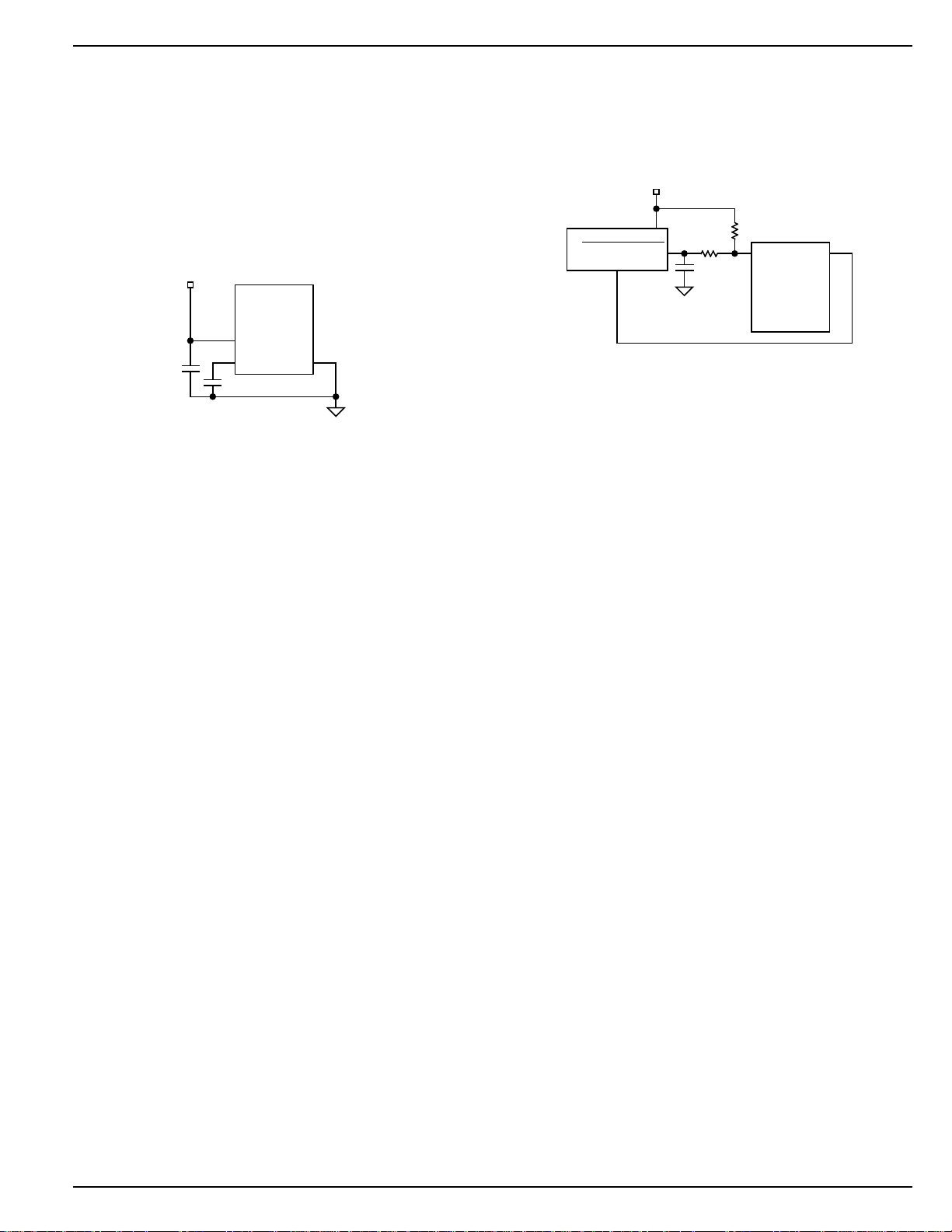
A 0.1µF to 1µF bypass capacitor from IN to GND, located at
the device, is strongly recommended to control supply transients. See Figure 1. Without a bypass capacitor, an output
short may cause sufficient ringing on the input (from supply
lead inductance) to damage internal control circuitry.
Input or output transients must not exceed the absolute
maximum supply voltage (V
duration.
Regulator Output Capacitor
A 1µF output capacitor is required between 3VOUT and GND
to prevent oscillation. Larger values improve the regulator’s
transient response. The output capacitor value may be increased without limit.
The output capacitor should have an ESR (effective series
resistance) of about 5Ω or less and a resonant frequency
above 1MHz. Most tantalum or aluminum electrolytic capacitors are adequate. Film types will work but are more expensive. Since many aluminum electrolytics have electrolytes
that freeze at about –30°C, solid tantalums are recommended for operation below –25°C.
The regulator will remain stable and in regulation with no load
other than the internal voltage divider, unlike many other
voltage regulators.
Switch Enable Input
EN must be driven logic high or logic low for a clearly defined
input. Floating the input may cause unpredictable operation.
EN should not be allowed to go negative with respect to GND.
Regulator Enable Input
Forcing 3VEN (regulator enable/shutdown) high enables the
regulator. Like EN, 3VEN is compatible with CMOS logic
gates.
If the enable/shutdown feature is not required, connect 3VEN
to IN.
Transient Overcurrent Fault-Flag Filter
When the MIC2529 is enabled, large values of capacitance
at the output of the device may cause inrush currents to flow
that exceed the short circuit current-limit threshold of the
device and cause the flag to activate. The duration of this time
depends on the size of the output capacitance. Refer to
June 1999 9 MIC2529
IN(max)
4.0V to 5.5V
0.1µF
to
1µF
MIC2529
18
FLG
27
OUT
36
IN
45
3VOUT
1µF
EN
OUT
3VEN
GND
Figure 1. Supply Bypassing
“Functional Characteristics: Switch Turn-On and Turnoff
Characteristics” for details. During the charging time, the
device enters into constant-current mode and the flag is
activated. As the capacitance is charged, the current decreases below the short circuit current-limit threshold and the
flag will be deasserted.
= 6V) even for a short
Figure 2. Transient Filter
In USB applications it is required that output bulk capacitance, shown in “Typical Application,” is utilized to meet
transient regulation requirements during hot-plug events.
When the MIC2529 is enabled into this capacitive load, the
flag may go active for about 200µs. Additionally, during hotplug events, inrush currents will also cause the flag to go
active for approximately 30µs. Since these conditions are not
valid overcurrent faults, the USB controller must ignore the
flag during these events. To prevent this erroneous overcurrent reporting, a 1ms RC filter must be used (see Figure 2).
Bus-Powered Hub Applications
The MIC2529 was designed for self-powered or bus-powered hubs. The integrated regulator reduces cost and space
in applications using a 3.3V USB controller. For self-powered
hubs, the MIC2529 will support 1 downstream port. For buspowered hubs, the MIC2529 will support up to four ganged
downstream ports.
Bus-Powered Hub Port Switching
The USB Specification requires that bus-powered hubs implement port switching on either a ganged or individual basis.
The specific implementation must be reported via the Hub
Descriptor Status Register. Individual port switching does
have some advantages in that a fault on one port will not
prevent the other ports from operating correctly. In addition,
a soft-start circuit must be included in order to reduce inrush
currents when the switch is enabled. To meet this requirement, the MIC2529 has been designed to slowly ramp its
output.
The USB Specification does not require bus-powered hubs to
report overcurrent conditions to the host since the hub is
already current-limited at the upstream port. However, if it is
desired to report overcurrent, the Hub Descriptor Status
Register must be programmed to indicate this. The MIC2529
provides a flag output for this application.
Page 10

MIC2529 Micrel
Suspend Current
Universal Serial Bus Specification
pend current requirement of 500µA on devices. For hubs,
Universal Serial Bus Specification Revision 1.1
issue. Revision 1.1, section 7.2.3, stipulates that the maximum suspend current for a configured hub is 2.5mA.
This number is derived by allocating 500µA for up to four
downstream ports plus 500µA for the hub’s internal functions.
A nonconfigured hub is considered a low-power device and
cannot consume more than 500µA. In a nonconfigured state
all downstream devices will be switched off. In most cases, a
nonconfigured hub is not a practical state for the system.
Therefore, the 2.5mA specification is the applicable target
specification for the suspend state. In a bus-powered hub
with less than 4 ports, the hub may use the additional current
for internal functions.
places a maximum sus-
clarifies this
The 500µA worst-case suspend current must be further
divided among the data port termination resistors and internal
functions. The termination resistors will consume
3.6V ÷ (16.5kΩ – 5%) = 230µA worst case. This leaves only
270µA for internal functions. Assuming 100µA as the maximum USB controller suspend current, 170µA remains for the
rest of the system. The MIC2529 will consume 150µA maximum, leaving a margin of 20µA.
USB Voltage Regulation
USB specifications require a minimum downstream voltage
supply of 4.40V from a bus-powered hub port (see
tion Note 17
100mV drop across the hub, leaving 250mV for PCB, upstream cable, and connector resistance. Therefore, the onresistance of the switch for each port, not including PCB
resistance, must be about 100mV ÷ 100mA = 1Ω. For a 4-port
ganged hub, this resistance reduces to 250mΩ. The MIC2529
easily satisfies this requirement.
for details). The USB specification allows for a
Applica-
MIC2529 10 June 1999
Page 11
MIC2529 Micrel
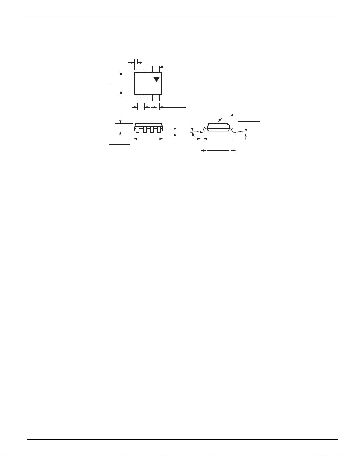
Package Information
0.026 (0.65)
MAX)
PIN 1
0.157 (3.99)
0.150 (3.81)
0.050 (1.27)
0.064 (1.63)
0.045 (1.14)
TYP
0.197 (5.0)
0.189 (4.8)
DIMENSIONS:
INCHES (MM)
0.020 (0.51)
0.013 (0.33)
0.0098 (0.249)
0.0040 (0.102)
0°–8°
SEATING
PLANE
8-Pin SOIC (M)
45°
0.050 (1.27)
0.016 (0.40)
0.244 (6.20)
0.228 (5.79)
0.010 (0.25)
0.007 (0.18)
June 1999 11 MIC2529
 Loading...