

Page 1
MIC2505/2506 Micrel
MIC2505/2506
Single 2A / Dual 1A / High-Side Switches
General Description
The MIC2505, MIC2505-1, MIC2505-2, and MIC2506 are
single and dual integrated high-side power switches that
consist of TTL compatible control/enable inputs, a charge
pump, and protected N-channel MOSFETs. The MIC2505/6
family can be used instead of separate high-side drivers and
MOSFETs in many low-voltage applications.
The MIC2505/6 family controls voltages ranging from 2.7V to
7.5V. The MIC2505-series can deliver at least 2A continuous
current while the MIC2506 can deliver at least 1A continuous
current from each output. A slow turn-on feature prevents
high inrush current when switching capacitive loads. The
internal control circuitry is powered from the same 2.7V to
7.5V. Within the device’s input range, outputs can be forced
higher than the input voltage when disabled.
Multipurpose open-drain fault flag outputs indicate overcurrent limiting, open-load detection (except MIC2505-1 and -2
versions), thermal shutdown, or undervoltage lockout for
each channel.
Overcurrent limiting is internally fixed and requires no external components.
Open-load detection is active when the switch is off. When
off, a normal load pulls the output pin low. If the load is open,
an optional, external, high-value resistor pulls the output pin
high, triggering the fault flag. MIC2505-1 and -2 versions are
tailored to Universal Serial Bus (USB) applications and do not
include open-load detection.
Thermal shutdown turns off the output if the die temperature
exceeds approximately 135°C. If enabled, the switch automatically restarts when the temperature falls 10°C.
Undervoltage lockout (UVLO) shuts off the output if the
supply drops below 2.3V typical and reenables the output
when the supply exceeds 2.5V typical.
Features
• Low MOSFET on resistance to 2.7V
30mΩ typical at 5V (MIC2505-series)
35mΩ typical at 3.3V (MIC2505-series)
75mΩ typical at 5V (each MIC2506 output)
80mΩ typical at 3.3V (each MIC2506 output)
• 2.7V to 7.5V input
• 110µA typical on-state supply current
•1µA typical off-state supply current
• Output can be forced higher than input (off-state)
• Current limit
• Thermal shutdown
• 2.5V undervoltage lockout (UVLO)
• Open-load detection
(MIC2505BN/M and MIC2506BN/M only)
• Open-drain fault flag
• 5ms (slow) turn-on and fast turnoff
• Logic-level control/enable input
Applications
• USB Power Distribution
• 3.3V and 5V power management
• PC Card card inrush limiting switch
• Hot plug-in power supplies
• Battery-charger circuits
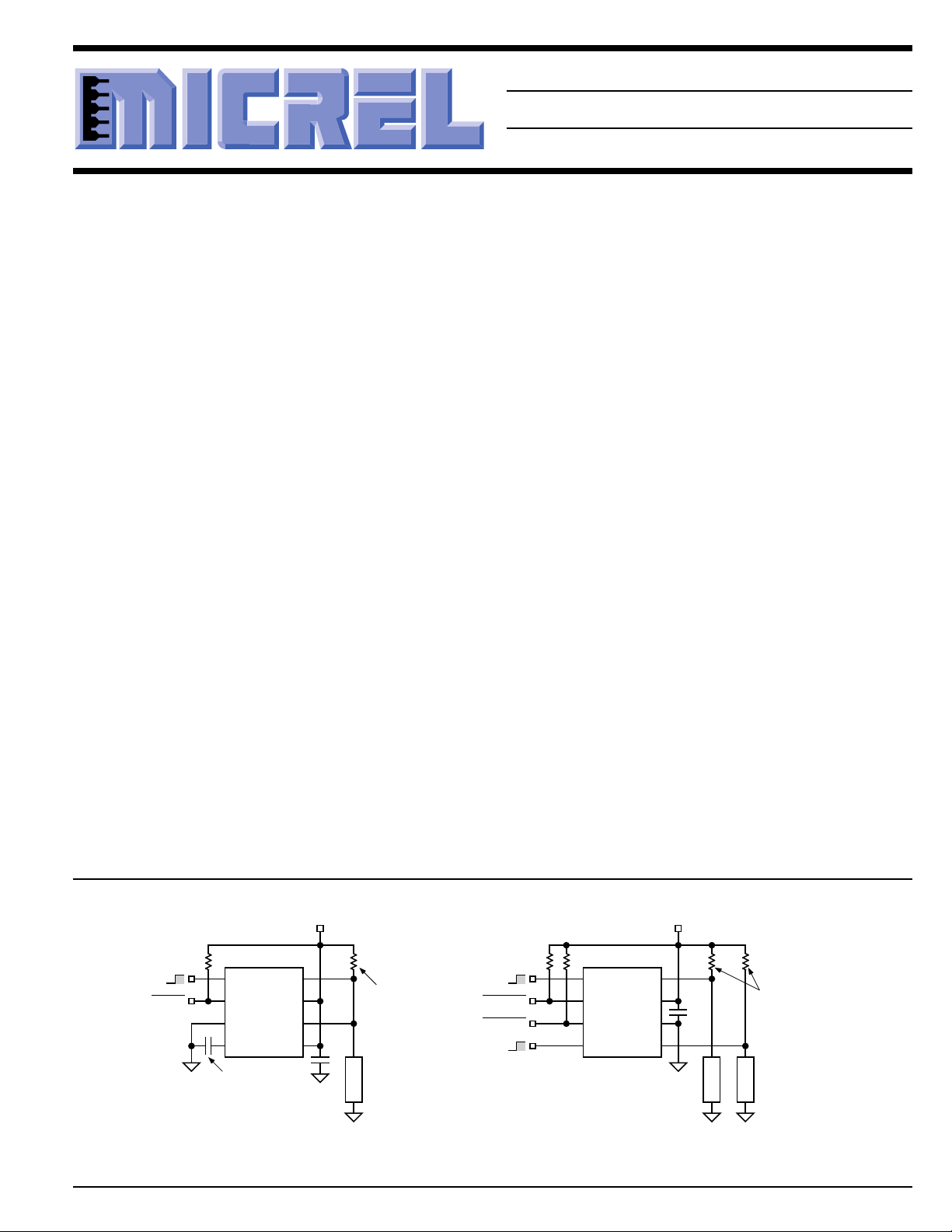
Typical Applications
2.7V to 7.5V
Resistors
(100k each)
A ON
A OFF
FAULT B
B ON
B OFF
Pull-up
MIC2506BM
18
CTL A OUT A
27
FLG A
36
FLG B GND
45
CTL B OUT B
ON
OFF
Pull-up
Resistor
(100k)
MIC2505BM
18
CTL OUT
27
FLG
36
GND OUT
45
GATE IN
Optional
Output Delay
Capacitor
INFAULT
0.1µF
100k
Optional
Open Load
Detect Resistor
(MIC2505BN or
MIC2505BM
only)
Load
Single and Dual Switch/Circuit Breakers with Open-Load Detection and Fault Output
April 1998 1 MIC2505/2506
2.7V to 7.5V
INFAULT A
0.1µF
100k 100k
Optional
Open Load
Detect Resistors
Load B
Load A
Page 2
MIC2505/2506 Micrel
Ordering Information
Part Number Control/Enable Open-Load Detect Temperature Range Package
Single-Switch
MIC2505BM Active-High Yes –40°C to +85°C 8-pin SOIC
MIC2505BN Active-High Yes –40°C to +85°C 8-pin DIP
MIC2505-1BM Active-High No –40°C to +85°C 8-pin SOIC
MIC2505-1BN Active-High No –40°C to +85°C 8-pin DIP
MIC2505-2BM Active-Low No –40°C to +85°C 8-pin SOIC
MIC2505-2BN Active-Low No –40°C to +85°C 8-pin DIP
Dual Switch
MIC2506BM Active-High Yes –40°C to +85°C 8-pin SOIC
MIC2506BN Active-High Yes –40°C to +85°C 8-pin DIP
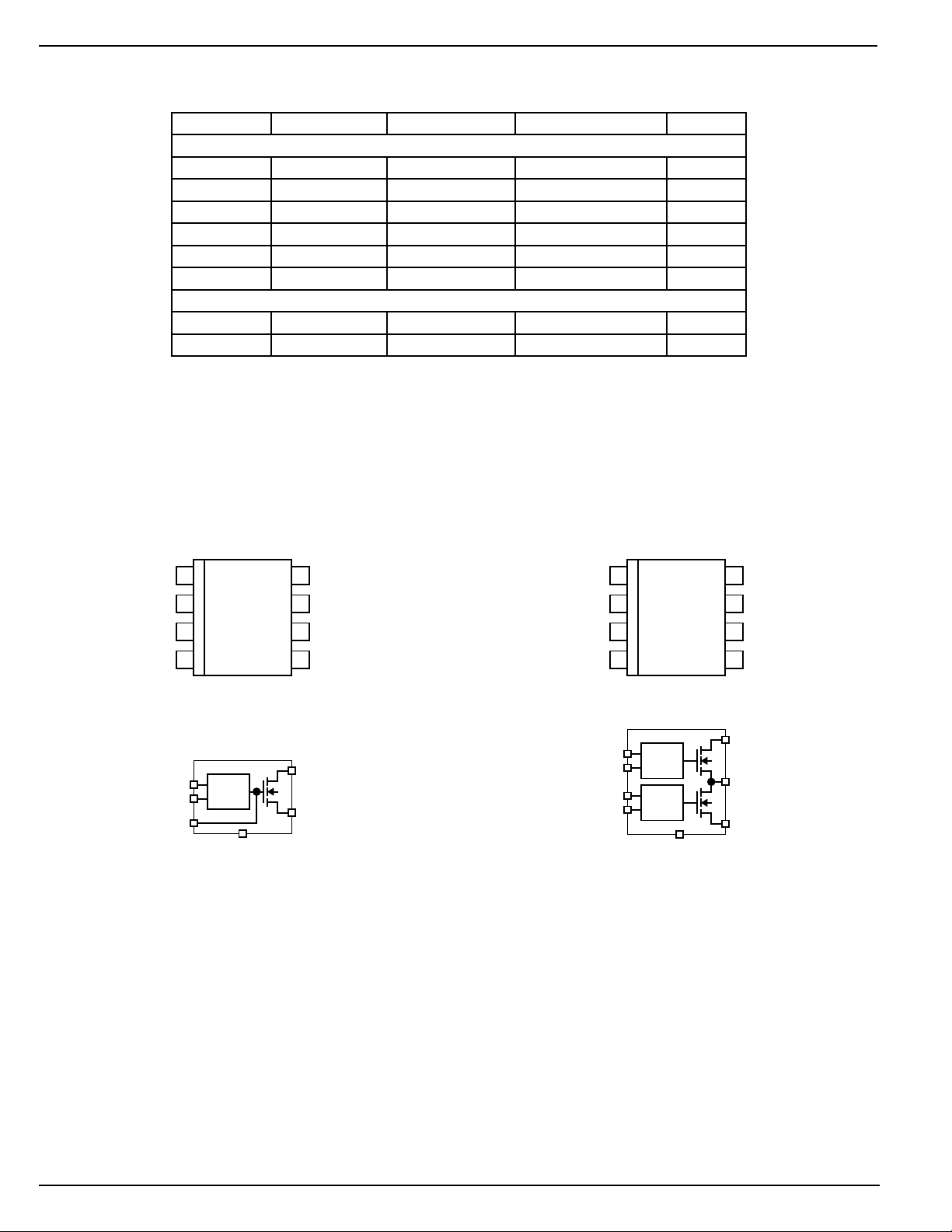
Pin Configuration
MIC2505/-1/-2
CTL
1
FLG
2
3
GND
GATE
(CTL A) 1
(FLG A) 2
(GATE A) 4
4
8-Pin SOIC (M)
8-Pin DIP (N)
MIC2505/-1/-2
LOGIC,
CHARGE
PUMP
3 (GND)
OUT
8
IN
7
OUT
6
IN
5
6, 8 (OUT)
5, 7 (IN)
CTL A
FLG A
FLG B
CTL B
(CTL A) 1
(FLG A) 2
(FLG B) 3
(CTL B) 4
MIC2506
1
2
3
4
MIC2506
LOGIC,
CHARGE
PUMP
LOGIC,
CHARGE
PUMP
6 (GND)
8-Pin SOIC (M)
8-Pin DIP (N)
OUT A
8
IN
7
GND
6
OUT B
5
8 (OUT A)
7 (IN)
5 (OUT B)
MIC2505/2506 2 April 1998
Page 3
MIC2505/2506 Micrel
Pin Description
Pin Number Pin Number Pin Name Pin Function
MIC2505 series
1 1 / 4 CTL (A/B) Control (Input): TTL compatible control input. High input typically > 1.8V.
2 2 / 3 FLG (A/B) Fault Flag (Output): Active-low, open-drain output. If CTL is low, indicates
3 6 GND Ground: Return.
4 — GATE Output MOSFET Gate: Open for fastest rise time. Connect capacitor to
5, 7 7 IN Supply Input: Output MOSFET drain. Also supplies IC’s internal circuitry.
6, 8 8 / 5 OUT (A/B) Switch Output: Output MOSFET source. Typically connect to switched side
MIC2506
Low input typically < 1.6V. MIC2505, MIC2505-1 and MIC2506 are active
high. MIC2505-2 is active low.
open load. If CTL is high, indicates current limit, thermal shutdown, or
UVLO.
MIC2505-1 and -2 do not support open-load detect
ground to slow rise time. (See MIC2505 Turn-On Delay graph)
Connect to supply.
MIC2505 series only:
of load. Output voltage can be pulled above input voltage in off mode.
MIC2505 series only:
Pins 5 and 7 must be externally connected together.
Pins 6 and 8 must be externally connected together.
.
Absolute Maximum Ratings
Supply Voltage (VIN) ....................................................8.0V
Fault Flag Voltage (V
Fault Flag Current (I
Output Voltage (V
Output Current (I
Gate Voltage (V
Control Input (V
OUT
OUT
GATE
CTL
).............................................7.5V
FLG
) ............................................50mA
FLG
) .................................................7.5V
)............................... Internally Limited
) ......................................... VIN + 15V
) ....................................... –0.3V to 15V
Operating Ratings
Supply Voltage (VIN) ................................... +2.7V to +7.5V
Ambient Operating Temperature (TA) ........–40°C to +85°C
Thermal Resistance
SOIC (θJA).........................................................160°C/W
DIP (θJA)............................................................105°C/W
Storage Temperature (TA) .......................–65°C to +150°C
Lead Temperature (Soldering 5 sec.) ....................... 260°C
April 1998 3 MIC2505/2506
Page 4

MIC2505/2506 Micrel
Electrical Characteristics
VIN = +5V; GATE = open; TA = 25°C, bold indicates –40°C ≤ TA ≤ +85°C; unless noted
Parameter Condition Min Typ Max Units
Supply Current MIC2505-1 V
MIC2506 V
MIC2505-2 V
Control Input Voltage V
Control Input Current V
Control Input Capacitance 1pF
Output MOSFET Resistance MIC2505 series V
MIC2506 V
Output Turn-On Delay MIC2505 series RL = 10Ω, C
MIC2506 RL = 10Ω each output 100 700 2000 µs
Output Turn-On Rise Time MIC2505 series RL = 10Ω, C
MIC2506 RL = 10Ω each output 200 2000 6000 µs
Output Turnoff Delay MIC2505 series RL = 10Ω, C
MIC2506 RL = 10Ω each output 0.8 20 µs
Output Turnoff Fall Time MIC2505 series RL = 10Ω, C
MIC2506 RL = 10Ω each output 0.7 20 µs
Output Leakage Current 10 µA
Current Limit Threshold MIC2505 series 2 4A
MIC2506 1 23A
Open Load Threshold, Note 1 V
Overtemperature Shutdown T
Threshold TJ decreasing 125 °C
Error Flag Output Resistance V
Error Flag Off Current V
UVLO Threshold V
= logic 0, OUT = open 0.75 5 µA
CTL
= logic 1, OUT = open 110 160 µA
CTL
= logic 0, OUT = open 110 160 µA
CTL
V
= logic 1, OUT = open 0.75 5 µA
CTL
= logic 0 → logic 1 transition 2.1 2.4 V
CTL
V
= logic 1 → logic 0 transition 0.8 1.9 V
CTL
= logic 0 0.01 1 µA
CTL
V
= logic 1 0.01 1 µA
CTL
= 5V, TA = 25°C3050 mΩ
IN
= 5V, –40°C < TA < +85°C 60 mΩ
V
IN
V
= 3.3V, TA = 25°C3560 mΩ
IN
VIN = 3.3V, –40°C < TA < +85°C 75 mΩ
= 5V, TA = 25°C75125 mΩ
IN
V
= 5V, –40°C < TA < +85°C 150 mΩ
IN
= 3.3V, TA = 25°C80135 mΩ
V
IN
VIN = 3.3V, –40°C < TA < +85°C 165 mΩ
= 0 200 850 2000 µs
GATE
= 0 500 3000 7500 µs
GATE
= 0 0.7 20 µs
GATE
= 0 1.5 20 µs
GATE
= logic low, Note 2 0.5 1 1.5 V
CTL
increasing 135 °C
J
= 5V, IL = 10mA 10 25 Ω
IN
VIN = 3.3V, IL = 10mA 15 40 Ω
= 5V 0.01 1 µA
FLAG
= increasing 2.2 2.5 2.7 V
IN
VIN = decreasing 2.0 2.3 2.5 V
General Note: Devices are ESD protected, however, handling precautions recommended.
General Note: All limits guaranteed by testing or statistical analysis.
Note 1: MIC2505-1 and -2 versions have no open load detect feature.
Note 2: Open-load threshold is the output voltage (V
resistor to VIN.
) where FLG becomes active (low) when CTL is low. OUT is pulled high by a 100k external
OUT
MIC2505/2506 4 April 1998
Page 5
MIC2505/2506 Micrel
0
20
40
60
80
100
2345678
OUTPUT RESISTANCE (mΩ)
SUPPLY VOLTAGE (V)
0
20
40
60
80
100
-40 -20 0 20 40 60 80 100
ON RESISTANCE (mΩ)
TEMPERATURE (°C)
0
0.5
1.0
1.5
2.0
2345678
SUPPLY CURRENT (µA)
SUPPLY VOLTAGE (V)
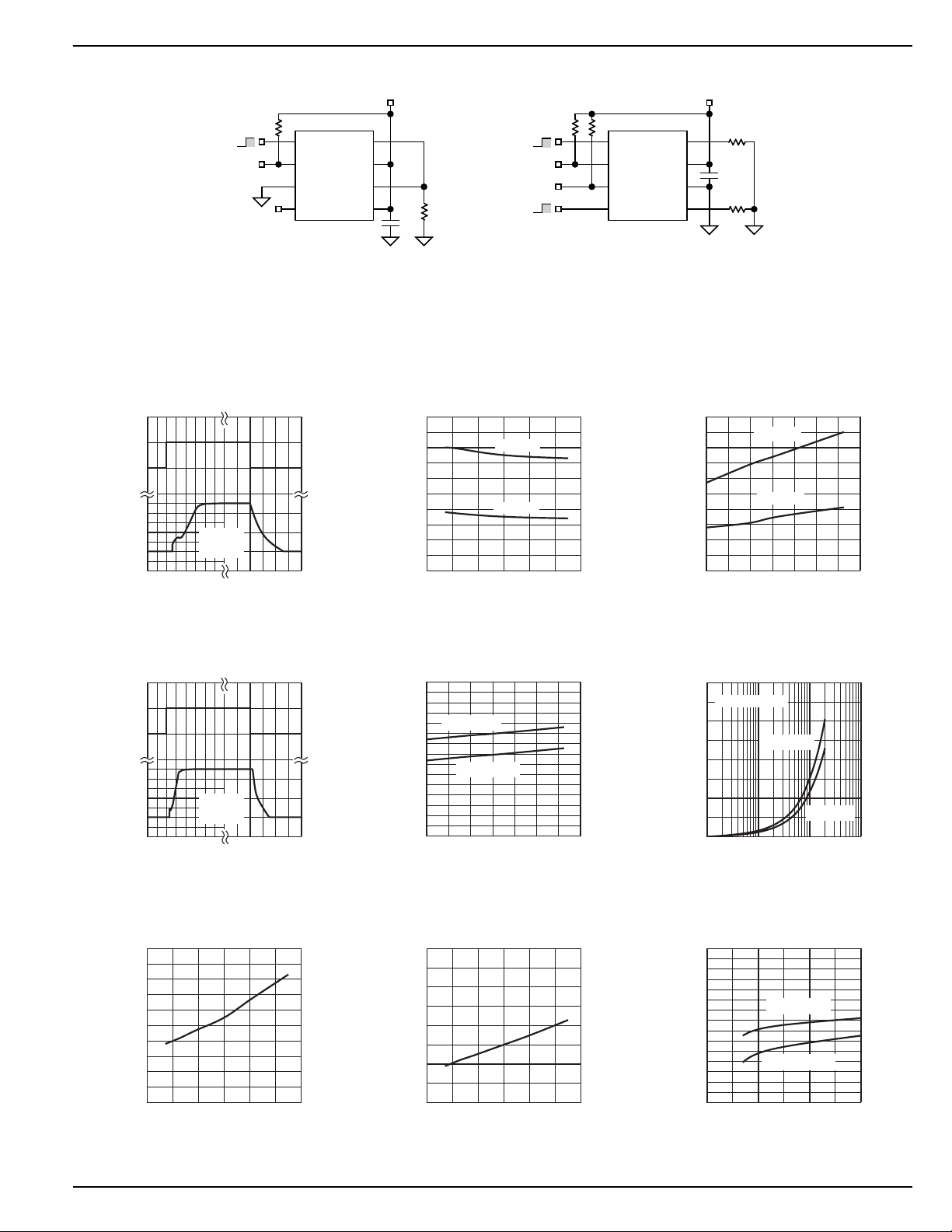
Test Circuits
GND
+5V
10Ω
IN
1µF
10Ω
+5V
10kΩ
10kΩ
V
FLG
MIC2505/-1/-2
CTL OUT
FLG
GND OUT
GATE IN
10kΩ
A ON
A OFF
B ON
B OFF
V
V
FLG A
FLG B
IN
10Ω
1µF
MIC2506BM
CTL A OUT A
FLG A
FLG B
CTL B OUT B
Typical Characteristics Note 2
MIC2505 Turn-On, Turnoff
Characteristics
10
5
0
CONTROL (V)
6
-5
4
2
0
OUTPUT (V)
-2
-2 0246
TIME (ms)
RL = 5Ω
= 1A)
(I
L
-2 024
TIME (µs)
MIC2506 Turn-On, Turnoff
Characteristics
10
5
0
CONTROL (V)
6
-5
4
2
0
OUTPUT (V)
-2
-2 0246
TIME (ms)
RL = 5Ω
= 1A)
(I
L
-1 012
TIME (µs)
Output On Resistance
vs. Supply Voltage
MIC2506
MIC2505
UVLO Threshold Voltage
3.0
2.5
2.0
THRESHOLD VOLTAGE (V)
1.5
vs. Temperature
VIN RISING
VIN FALLING
-40 -20 0 20 40 60 80 100
TEMPERATURE (°C)
Output On Resistance
vs. Temperature
MIC2506
MIC2505
Error Flag Voltage
vs. Error Flag Current
400
FLG = ACTIVE
300
VDD = 3.3V
200
100
ERROR FLAG VOLTAGE (mV)
0
0.1 1 10 100
ERROR FLAG CURRENT (mA)
VDD = 5V
On-State Supply Current
200
180
160
140
120
100
April 1998 5 MIC2505/2506
80
60
40
SUPPLY CURRENT (µA)
20
0
2345678
vs. Supply Voltage
SUPPLY VOLTAGE (V)
Off-State Supply Current
vs. Supply Voltage
Control Threshold
vs. Supply Voltage
2.5
2.0
1.5
THRESHOLD VOLTAGE (V)
1.0
2345
V
RISING
CTL
V
FALLING
CTL
SUPPLY VOLTAGE (V)
Page 6
MIC2505/2506 Micrel
On-State Supply Current
200
180
160
140
120
100
SUPPLY CURRENT (µA)
vs. Temperature
80
60
40
20
0
-40 -20 0 20 40 60 80 100
TEMPERATURE (°C)
Off-State Supply Current
2.0
1.5
1.0
0.5
SUPPLY CURRENT (µA)
vs. Temperature
0
-40 -20 0 20 40 60 80 100
TEMPERATURE (°C)
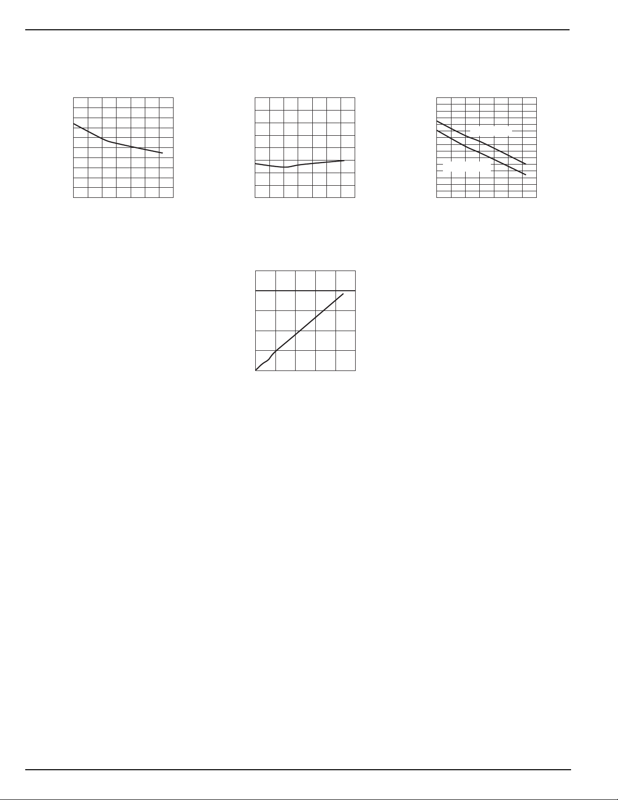
MIC2505 Turn-On Delay
with External Gate Capacitance
1000
800
600
400
200
TURN-ON DELAY (ms)
0
0 50 100 150 200 250
CAPACITANCE (nF)
Control Threshold
2.5
2.0
1.5
THRESHOLD VOLTAGE (V)
vs. Temperature
V
RISING
CTL
V
FALLING
CTL
1
-40 -20 0 20 40 60 80 100
TEMPERATURE (°C)
MIC2505/2506 6 April 1998
Page 7
MIC2505/2506 Micrel
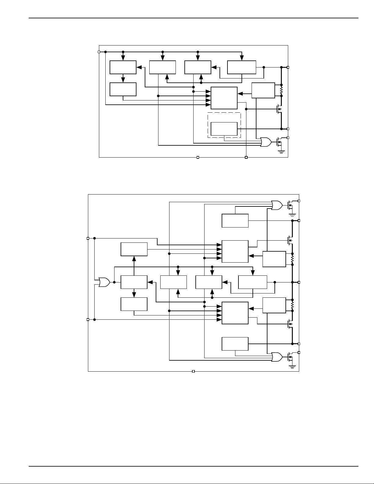
Block Diagrams
CTL
CTL A
OSC.
CHARGE
PUMP
MIC2505/2505-1/2505-2
CHARGE
PUMP
THERMAL
SHUTDOWN
UVLO
REFERENCE
GATE
CONTROL
Not Included in
MIC2505-1, -2
OPEN LOAD
DETECT
MIC2505-Series Block Diagram
OPEN LOAD
DETECT
GATE
CONTROL
1.2V
GATEGND
CURRENT
LIMIT
CURRENT
IN
OUT
FLG
FLG A
OUT A
LIMIT
CTL B
MIC2506
OSC.
CHARGE
PUMP
THERMAL
SHUTDOWN
UVLO
OPEN LOAD
GND
MIC2506 Block Diagram
REFERENCE
GATE
CONTROL
DETECT
1.2V
CURRENT
LIMIT
IN
OUT B
FLG B
April 1998 7 MIC2505/2506
Page 8

MIC2505/2506 Micrel
Functional Description
The MIC2505-series and MIC2506 are high-side N-Channel
switches. The MIC2505, MIC2505-1, and MIC2506 have
active-high enable inputs. The MIC2505-2 has an active-low
input. Fault conditions inhibit output transistor turn-on or
turnoff when enabled.
Control Input
CTL (control input) activates the oscillator, thermal shutdown, UVLO, 1.2V reference, and gate control circuits. If
there are no fault conditions, the output MOSFET turns on
when enabled.
Reference
A 1.2V bandgap reference supplies a regulated voltage to the
thermal shutdown and undervoltage lockout circuits. The
reference is only active when CTL is enabled.
Oscillator/Charge Pump
The oscillator produces an 80kHz square wave output which
drives the charge pump. The oscillator is enabled when CTL
is active.
The charge pump is a voltage quintupler (5×). The charge
pump capacitors are self contained.
Gate Control
The gate control circuit charges the output MOSFET gate
from the charge pump output or discharges the MOSFET
gate to ground as determined by CTL, thermal shutdown, or
UVLO (undervoltage lockout).
An optional, external capacitor may be connected to the
MIC2505 GATE to lengthen the rise time. This slows the turn
on of the MOSFET output switch. (See “MIC2505 Turn-On
Delay” graph.) Since this pin connects directly to the MOSFET
gate, use ESD precautions when contacting components
connected to this pin. Leakage resistance may increase turnon times.
Input and Output
IN (input) is the supply connection to the logic circuitry and the
drain of the output MOSFET. OUT (output) is the source of the
output MOSFET. In a typical circuit, current flows through the
switch from IN to OUT toward the load.
The output MOSFET and driver circuitry are also designed to
allow the MOSFET source to be externally forced to a higher
voltage than the drain (V
off and VIN > UVLO minimum. In this situation, the MIC2505/6
avoids undesirable drain to body diode reverse current flow
by grounding the body when the switch is off. (The conventional method for optimum turn-on threshold has the source
connected to the body. This would allow a large current to flow
when V
source
> V
drain
MIC2505 Series Only
> VIN) when the output switch is
OUT
+ 0.6V.)
Duplicate IN and OUT leads are not internally connected.
Connect both IN pins to the supply. Connect both OUT leads
to the load.
Thermal Shutdown
Thermal shutdown shuts off the output MOSFET and signals
the fault flag if the die temperature exceeds 135°C. 10°C of
hysteresis prevents the switch from turning on until the die
temperature drops to 125°C.
Overtemperature detection functions only when the control
input is enabled (output MOSFET is on). Both MIC2506
outputs are shut off during overtemperature, and both flags
will go low.
Undervoltage Lockout
UVLO (undervoltage lockout) prevents the output MOSFET
from turning on until VIN (input voltage) exceeds 2.5V typical.
After the switch turns on, if VIN drops below 2.3V typical,
UVLO shuts off the output MOSFET and turns the fault flag
on (active low) until VIN drops below 1.5V.
Undervoltage detection functions only when the control input
is enabled (output MOSFET is on).
Overcurrent Limit
The overcurrent limit is preset internally. The preset level
prevents damage to the output MOSFET but allows a minimum current of 2A through the output MOSFET of the
MIC2505-series and 1A for each output MOSFET of the
MIC2506. Output current is monitored by sensing the voltage
drop across the output MOSFET drain metal resistance.
Overcurrent detection functions only when the control input is
enabled (output MOSFET is on) and VIN is above the UVLO
threshold.
Open-Load Detection
Open-load detection is available only on the MIC2505 and
MIC2506. The open-load detection feature is not included in
the MIC2505-1 or -2 versions.
Open-load detection indicates the absence of an output load
by activating the fault flag. Open-load detection is optional
and is enabled by connecting a high-value pull-up resistor
between IN and OUT. If there is no load, the circuit detects a
high OUT (output) voltage (typically ≥1V) and signals the fault
flag. Under normal conditions, the low resistance of a typical
load pulls OUT low. Open-load detection functions only when
the control input is low (output MOSFET is off).
Fault Flag
FLG is an N-channel, open-drain MOSFET output. The faultflag is active (low) for one or more of the following conditions:
open load (except MIC2505-1 and -2 versions), undervoltage, current limit, or thermal shutdown. The flag output
MOSFET is capable of sinking a 10mA load to typically
100mV above ground.
MIC2505/2506 8 April 1998
Page 9
MIC2505/2506 Micrel
Applications Information
Supply Filtering
A 0.1µF to 1µF bypass capacitor from IN to GND, located at
the device is strongly recommended to control supply transients. Without a bypass capacitor, an output short may
cause sufficient ringing on the input (from supply lead inductance) to destroy the internal control circuitry.
Input transients must not exceed the absolute maximum
supply voltage (V
ON
OFF
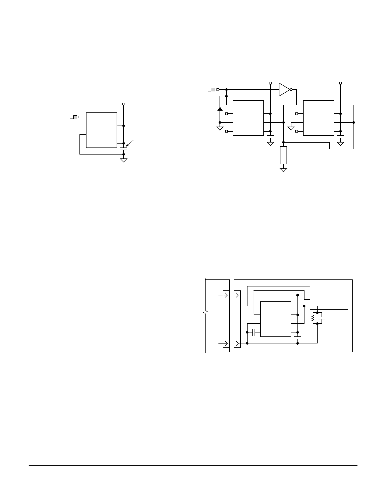
Figure 1. Supply Bypassing
The bypass capacitor may be omitted only if board design
precautions are followed, such as using extremely short
supply leads or power and ground planes.
Control Input
CTL must be driven logic high or logic low, or be pulled high
or low for a clearly defined input. Floating the input may cause
unpredictable operation. Add a diode clamp if negative spikes
may occur. See Figure 2.
Open-Load Detection
Refer to “Typical Applications” (first page). Open-load detection is available only on the MIC2505 and MIC2506. For USB
power distribution applications, the open-load detection feature is not included in the MIC2505-1 or -2 versions.
The optional open-load detection resistor supplies a small
pull-up current to the load when the output switch is off. (A
100k resistor will draw 50µA from a 5V supply.) Normally, the
load dominates, pulling OUT low. If the load is absent, the
optional resistor pulls OUT high, activating the fault flag if CTL
is off.
When a load is switched off with CTL, capacitance on the
output may cause the open-load function to pull the flag low
until the capacitor is discharged below approximately 2.4V.
Omit the pull-up resistor when open load detection is not
required and for minimum off-state supply current.
Power Bus Switch
The MIC2505/6 family features a MOSFET reverse current
flow prevention circuit. This prevents current from flowing
backwards (from OUT to IN) when CTL is disabled as long as
VIN is above UVLO minimum. In Figure 2, when U1 is on and
= 7.5V) even for a short duration.
IN max
2.7V to 7.5V
MIC2505BM
18
CTL OUT
27
FLG
36
GND OUT
45
GATE IN
IN
0.1µF to 1µF
U2 is off, this feature prevents current flow from the load (5V)
backward through U2 to the 3.3V supply. (If a discrete
MOSFET and driver were used, the MOSFET’s internal body
diode would short the 5V load to the 3.3V supply.)
FLG will be active (low) on any switch that is off whenever the
load voltage is greater than the open load threshold (approximately 1V) except for MIC2505-1 and MIC2505-2.
Logic-High = 5V Output
Logic-Low = 3.3V Output
1N4148
(optional)
+5V
U1
MIC2505BM
18
CTL OUT
27
FLG
36
GND OUT
45
GATE IN
IN
0.1µF
Load
U2
MIC2505BM
18
CTL OUT
27
FLG
36
GND OUT
45
GATE IN
+3.3V
IN
0.1µF
Figure 2. 5V/3.3V Switch Concept
This circuit’s function would otherwise require a dual driver,
two MOSFETs, plus two diodes (or a dual driver plus four
MOSFETs).
Hot Plug-In Applications (Soft-Start)
The MIC2505/6 family can be used to protect the socket-side
and card-side of a supply circuit from transients caused when
a capacitive load is connected to an active supply.
The switch presents a high impedance when off, and slowly
becomes a low impedance as it turns on. This reduces the
inrush current and related voltage drop that result from
charging a capacitive load.
Power Control
3.3V
GND
MIC2505BM
18
CTL OUT
27
FLG
36
GND OUT
45
GATE IN
CardSocket
IN
0.1µF
Circuitry
Capacitive
Load
Figure 3. Hot Plug-In Concept
A gate capacitor may be added to the MIC2505 to slow the
turn on time even more, reducing the inrush current. See
“MIC2505 Turn-On Delay” graph. The UVLO feature insures
that each time the card is removed and VIN = 0 that the gate
of the output switch is discharged to zero volts. A controlled
turn-on is executed each time a board is plugged in, even with
multiple insertions.
April 1998 9 MIC2505/2506
Page 10
MIC2505/2506 Micrel
Applications Information
USB Application
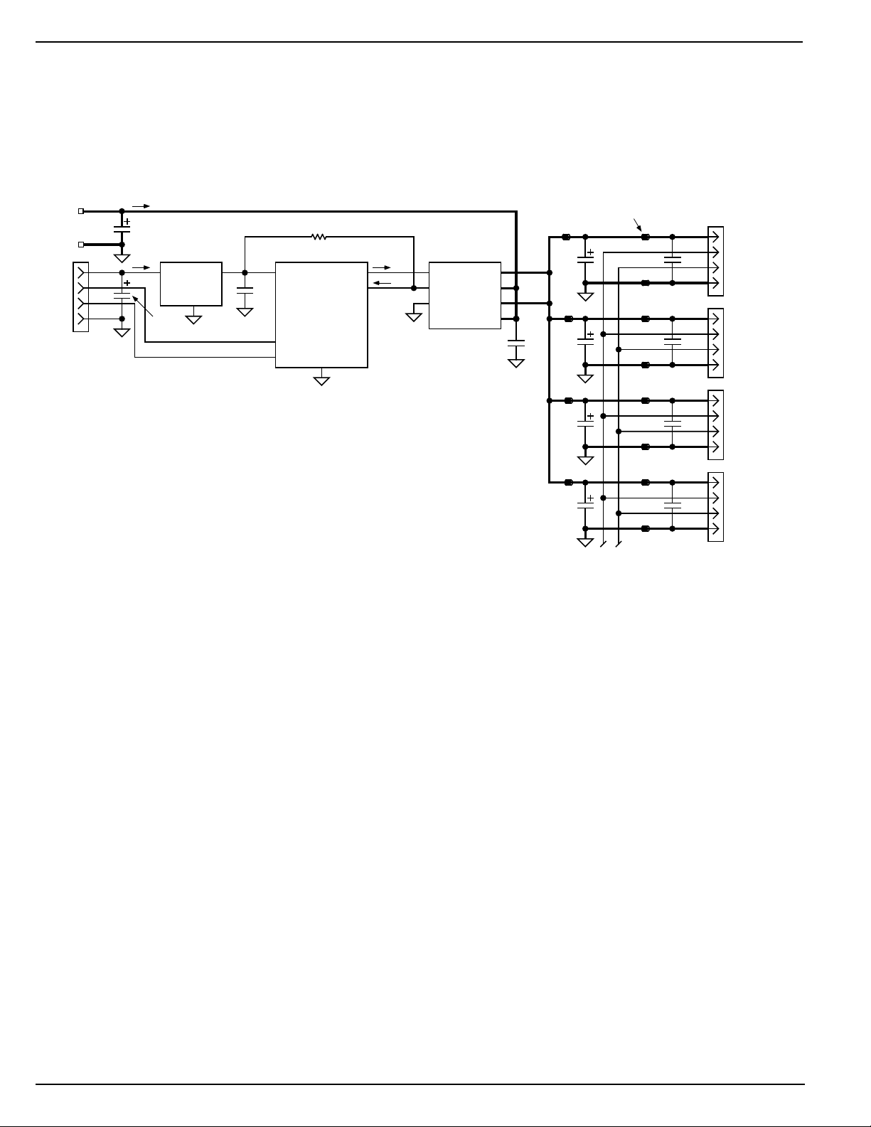
Figure 4 depicts a low cost and robust implementation of a
four-port, self-powered USB hub circuit employing ganged
overcurrent protection.
Ferrite
(+)
4.45V to 5.25V
3.5A max.
(–)
V
D+
D–
GND
BUS
33µF
MIC5203-3.3
MIC5207-3.3
LDO Regulator
IN OUT
4.7
µF
GND
V+
1.0
OVERCURRENT
µF
D+
D–
100k
GND
ON/OFF
MIC2505-2/-13.3V USB Controller
EN OUT
FLG IN
GND OUT
GATE IN
33µF
0.1µF
33µF
Bead
0.01µF
0.01µF
V
BUS
D+
D–
GND
V
BUS
D+
D–
GND
Downstream
USB
Port 1
500mA max.
Downstream
USB
Port 2
500mA max.
Bold lines indicate
0.1" wide, 1-oz. copper
high-current traces.
Figure 4. Ganged-Switch Self-Powered Hub
33µF
33µF
Data
0.01µF
0.01µF
V
BUS
D+
D–
GND
V
BUS
D+
D–
GND
Downstream
USB
Port 3
500mA max.
Downstream
USB
Port 4
500mA max.
MIC2505/2506 10 April 1998
Page 11
MIC2505/2506 Micrel
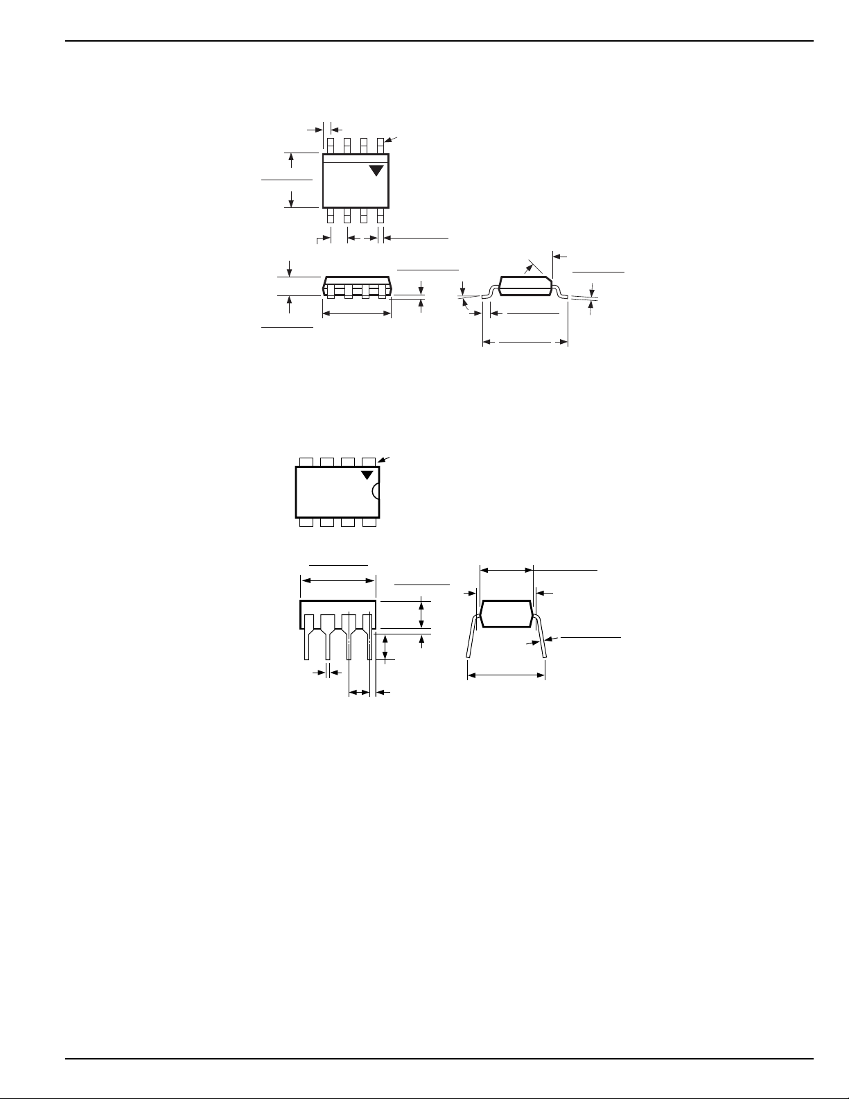
Package Information
0.026 (0.65)
MAX)
PIN 1
0.157 (3.99)
0.150 (3.81)
0.050 (1.27)
0.064 (1.63)
0.045 (1.14)
TYP
0.197 (5.0)
0.189 (4.8)
0.380 (9.65)
0.370 (9.40)
DIMENSIONS:
INCHES (MM)
0.020 (0.51)
0.013 (0.33)
0.0098 (0.249)
0.0040 (0.102)
0°–8°
SEATING
PLANE
8-Pin SOIC (M)
PIN 1
0.135 (3.43)
0.125 (3.18)
45°
0.050 (1.27)
0.016 (0.40)
0.244 (6.20)
0.228 (5.79)
DIMENSIONS:
INCH (MM)
0.010 (0.25)
0.007 (0.18)
0.255 (6.48)
0.245 (6.22)
0.300 (7.62)
0.018 (0.57)
0.100 (2.54)
0.130 (3.30)
0.0375 (0.952)
8-Pin DIP (N)
0.013 (0.330)
0.010 (0.254)
0.380 (9.65)
0.320 (8.13)
April 1998 11 MIC2505/2506
Page 12

MIC2505/2506 Micrel
MICREL INC. 1849 FORTUNE DRIVE SAN JOSE, CA 95131 USA
TEL + 1 (408) 944-0800 FAX + 1 (408) 944-0970 WEB http://www.micrel.com
This information is believed to be accurate and reliable, however no responsibility is assumed by Micrel for its use nor for any infringement of patents or
other rights of third parties resulting from its use. No license is granted by implication or otherwise under any patent or patent right of Micrel Inc.
© 1998 Micrel Incorporated
MIC2505/2506 12 April 1998
 Loading...