

Page 1
General Description
MIC23250
4MHz Dual 400mA Synchronous Buck
Regulator with HYPER LIGHT LOAD™
Features
The MIC23250 is a high efficiency 4MHz dual 400mA
synchronous buck regulator with Hyper Light Load™. Hyper
Light Load™ provides all the advantages of standard light
load modes, such as low quiescent current and high
efficiency but also allows the use of very small output
capacitors to maintain low output ripple voltage throughout
the entire load range. This benefit is not possible with other
light load mode types as they trade off control speed for low
standby currents. With Hyper Light Load™, the output
capacitor can be reduced by up to a factor of 20 saving cost
and valuable board space. The tiny package (2mm x 2mm
Thin MLF
®
) of MIC23250 also saves crucial board space by
using only six external components while regulating two
independent outputs up to 400mA each.
The device is designed for use with a 1µH inductor and a
4.7µF output capacitor that enables a sub-1mm height.
The MIC23250 has a very low quiescent current of 35µA
and can achieve over 85% efficiency at 1mA. At higher
loads the MIC23250 provides a constant switching
frequency around 4MHz while providing peak efficiencies up
to 94%.
The MIC23250 fixed output voltage option is available in a
10-pin 2mm x 2mm Thin MLF
®
with a junction operating
range from –40°C to +125°C. The adjustable output voltage
option will soon be available in Q2/Q3 2008.
Data sheets and support documentation can be found on
Micrel’s web site at: www.micrel.com.
• Input voltage range: 2.7V to 5.5V
• Dual output current 400mA/400mA
• Hyper Light Load™ mode
– 35µA dual quiescent current
– 1µH inductor with a 4.7µF capacitor
• 4MHz in PWM operation
• Ultra fast transient response
• Low voltage output ripple
– 20mVpp in Hyper Light Load™ mode
– 3mV output voltage ripple in full PWM mode
• Up to 94% peak efficiency and 85% efficiency at 1mA
• Fully integrated MOSFET switches
• Micropower shutdown
• Thermal shutdown and current limit protection
• Fixed output:10-pin 2mm x 2mm Thin MLF
• Adjustable output:12-pin 2.5mm x 2.5mm Thin MLF
®
®
(Available in Q2/Q3 2008)
• –40°C to +125°C junction temperature range
Applications
• Mobile handsets
• Portable media players
• Portable navigation devices (GPS)
• WiFi/WiMax/WiBro modules
• Digital cameras
• Wireless LAN cards
• USB Powered Devices
___________________________________________________________________________________________________________
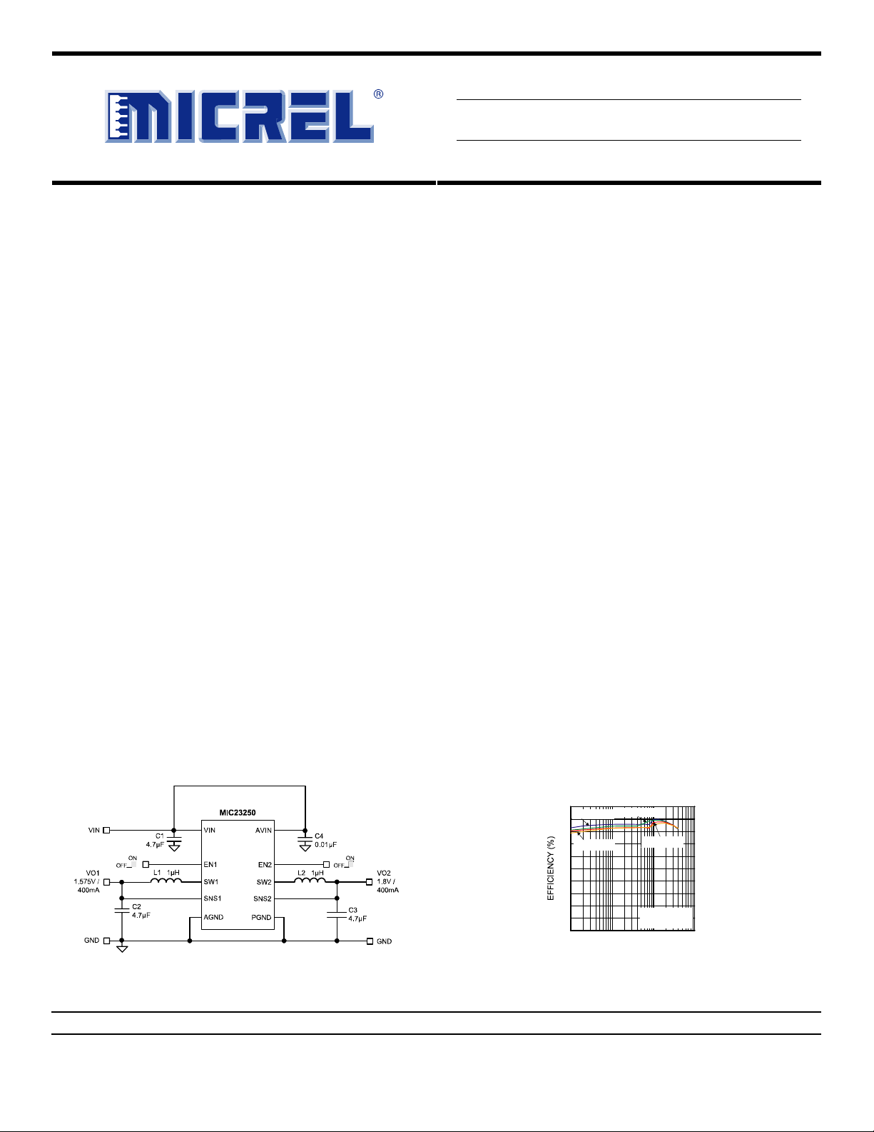
Typical Application
Hyper Light Load is a trademark of Micrel, Inc.
MLF and MicroLeadFrame are registered trademarks of Amkor Technology, Inc.
Micrel Inc. • 2180 Fortune Drive • San Jose, CA 95131 • USA • tel +1 (
December 2007
Efficiency V
100
VIN = 2.7V
90
80
70
VIN = 4.2V
60
50
40
30
20
10
0
1 10 100 1000
OUT
VIN = 3.0V
VIN = 3.6V
L = 1µH
C
LOAD (mA)
= 1.8V
OUT
= 4.7µF
408
) 944-0800 • fax + 1 (408) 474-1000 • http://www.micrel.com
M9999-121707-A
Page 2
Micrel, Inc. MIC23250
A
Ordering Information
Part Number Marking
MIC23250-GFHYMT WV1 1.575V 1.8V –40° to +125°C
MIC23250-G4YMT WV5 1.8V 1.2V –40° to +125°C
MIC23250-C4YMT WV2 1.0V 1.2V –40° to +125°C
MIC23250-3BYMT WV3 1.1V 0.9V –40° to +125°C
MIC23250-W4YMT WV4 1.6V 1.2V –40° to +125°C
MIC23250-Adj* TBD ADJ ADJ –40° to +125°C
Note: * Available Q2/Q3 2008
Nominal
Output
Voltage 1
Nominal
Output
Voltage 2
Junction
Temp. Range
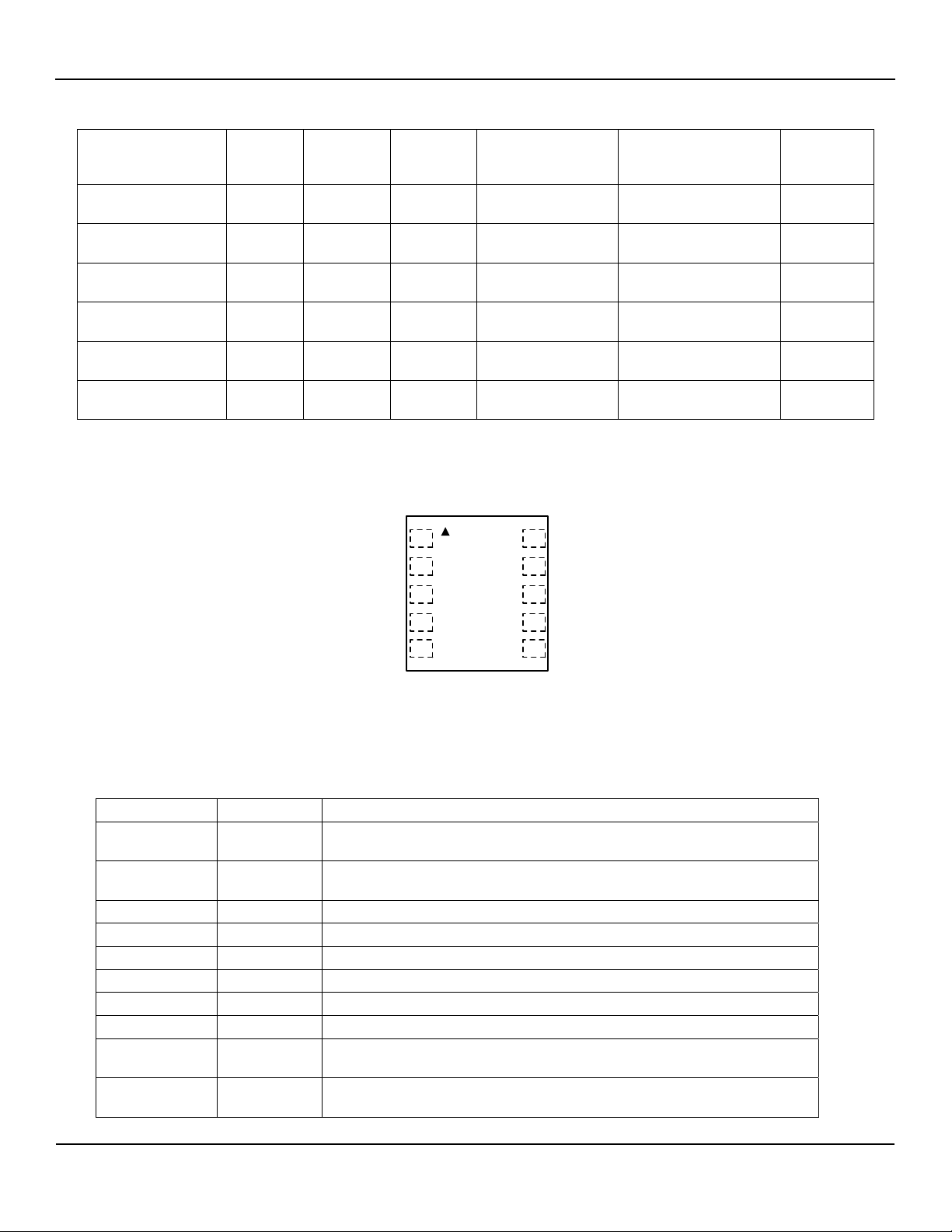
Pin Configuration
1SNS1
EN1
2
10 SNS2
EN2
9
Package
10-Pin 2mm x 2mm
Thin MLF
10-Pin 2mm x 2mm
Thin MLF
10-Pin 2mm x 2mm
Thin MLF
10-Pin 2mm x 2mm
Thin MLF
10-Pin 2mm x 2mm
Thin MLF
12-Pin 2.5mm x
2.5mm Thin MLF
®
®
®
®
®
®
Lead
Finish
Pb-Free
Pb-Free
Pb-Free
Pb-Free
Pb-Free
Pb-Free
Pin Description
Pin Number Pin Name Pin Name
1 SNS1
2 EN1
3 AGND Analog Ground. Must be connected externally to PGND.
4 SW1 Switch Node 1 (Output): Internal power MOSFET output.
5 PGND Power Ground.
6 VIN Supply Voltage (Power Input): Requires close bypass capacitor to PGND.
7 SW2 Switch Node 2 (Output): Internal power MOSFET output.
8 AVIN Supply Voltage (Power Input): Analog control circuitry. Connect to VIN.
9 EN2
10 SNS2
GND
SW1
PGND VIN5
3
4
AVIN
8
SW2
7
6
10-Pin 2mm x 2mm Thin MLF® (MT)
(Top View)
Sense 1 (Input): Error amplifier input. Connect to feedback resistor network to
set output 1 voltage.
Enable 1 (Input): Logic low will shut down output 1. Logic high powers up
output 1. Do not leave unconnected.
Enable 2 (Input): Logic low will shut down output 2. Logic high powers up
output 2. Do not leave unconnected.
Sense 2 (Input): Error amplifier input. Connect to feedback resistor network to
set output 2 voltage.
December 2007
2
M9999-121707-A
Page 3
Micrel, Inc. MIC23250
Absolute Maximum Ratings
(1)
Operating Ratings
(2)
Supply Voltage (VIN)......................................................... 6V
Output Switch Voltage (V
Logic Input Voltage (V
Storage Temperature Range (T
ESD Rating
(3)
.................................................................. 2kV
) ............................................ 6V
SW
) ..................................–0.3V to VIN
EN
)..............–65°C to +150°C
s
Supply Voltage (VIN)......................................... 2.7V to 5.5V
Logic Input Voltage (V
Junction Temperature (T
Thermal Resistance
2mm x 2mm Thin MLF
) .................................. –0.3V to VIN
EN
) ..................–40°C TJ +125°C
J
®
-10 (θJA)........................70°C/W
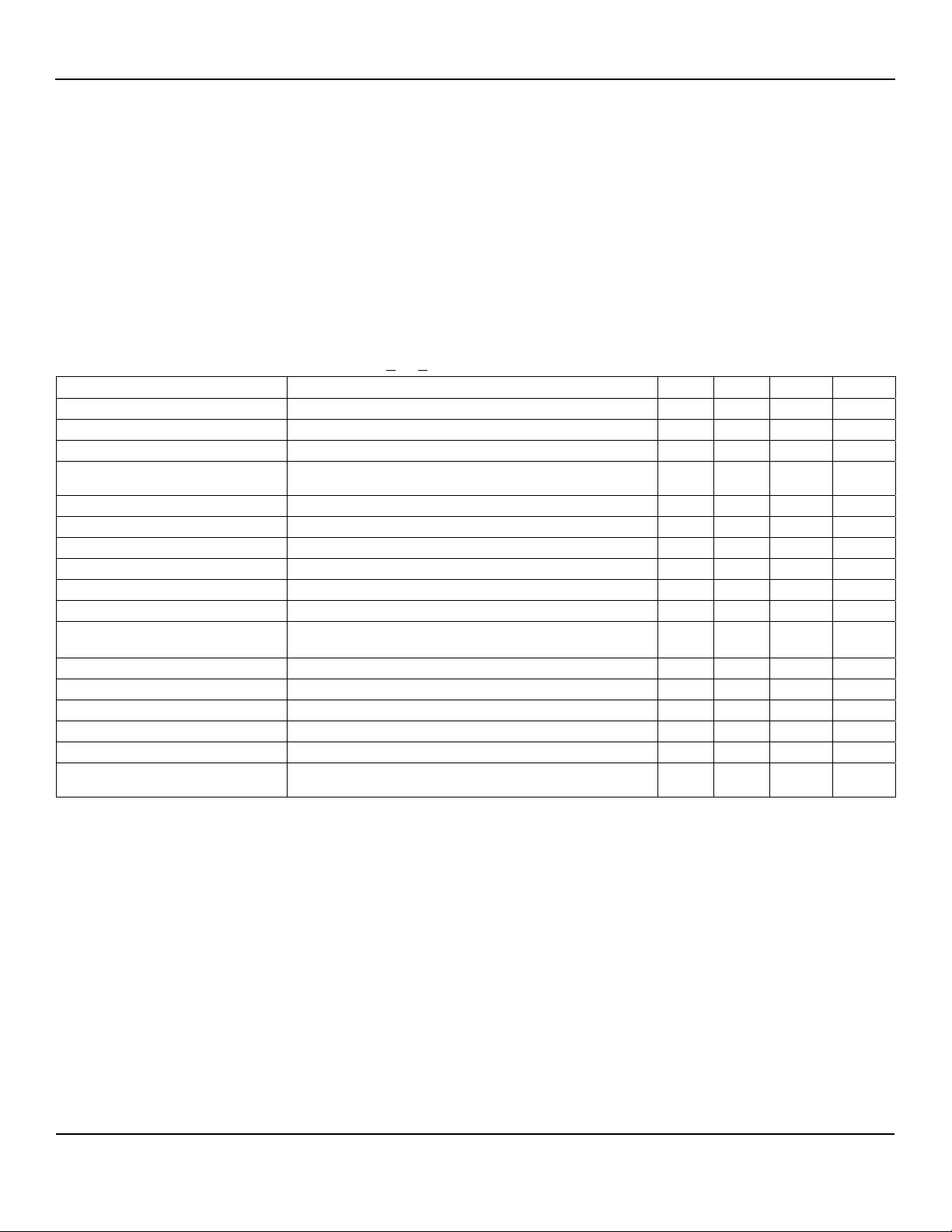
Electrical Characteristics
T
= 25°C with VIN = VEN = 3.6V; L = 1µH; C
A
otherwise specified. Bold values indicate –40°C< T
Parameter Condition Min Typ Max Units
Supply Voltage Range 2.7 5.5 V
Under-Voltage Lockout Threshold (turn-on) 2.45 2.55 2.65 V
UVLO Hysteresis 60 mV
Quiescent Current,
Hyper LL mode
Shutdown Current V
Output Voltage Accuracy VIN = 3.6V, I
Current Limit in PWM Mode SNS = 0.9*V
Output Voltage Line Regulation VIN = 3.0V to 5.5V, I
Output Voltage Load Regulation 20mA < I
Maximum Duty Cycle
PWM Switch ON-Resistance
Frequency I
Soft Start Time V
Enable Threshold
Enable Input Current 0.1
Over-temperature Shutdown 160
Over-temperature Shutdown
Hysteresis
Notes:
1. Exceeding the absolute maximum rating may damage the device.
2. The device is not guaranteed to function outside its operating rating.
3. Devices are ESD sensitive. Handling precautions recommended. Human body model: 1.5k in series with 100pF.
4. Specification for packaged product only.
(4)
= 4.7µF; I
OUT
< +125°C.
J
V
OUT1, 2 (both Enabled)
, I
OUT1, 2
Nominal
= 0V; VIN = 5.5V 0.01
EN1, 2
= 20mA
LOAD
OUT NOM
LOAD
< 400mA, VIN = 3.6V 0.5 %
LOAD
SNS ≤ V
= 100mA PMOS
I
SW
= -100mA NMOS
I
SW
LOAD
OUT
, V
NOM
= 1.8V, VIN = 2.7V
OUT
= 120mA
= 90% 260 µs
= 20mA; only one channel power is enabled, unless
OUT
= 0mA , SNS1, 2 >1.2 * V
OUT1, 2
35 50 µA
4
–2.5
0.410
0.65
+2.5
1
µA
%
A
= 20mA 0.4 %/V
80
3.4
0.5
86 %
0.6
0.8
4
0.8
4.6
1.2
2
MHz
V
µA
°C
40
°C
December 2007
3
M9999-121707-A
Page 4
Micrel, Inc. MIC23250
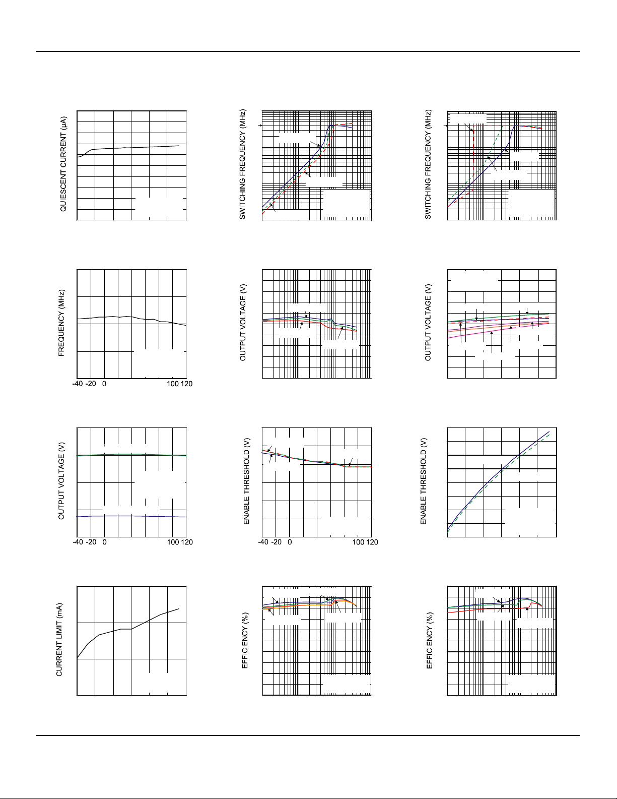
Typical Characteristics
Quiescent Current
vs. Input Voltage
50
45
40
35
30
25
20
15
10
5
0
2.7
3.2 3.7 4.2 4.7 5.2 5.7
5.0
4.5
4.0
3.5
3.0
1.9
1.8
1.7
1.6
1.5
700
650
600
550
2.7
3.2 3.7 4.2 4.7 5.2 5.7
December 2007
L = 1µH
C
= 4.7µF
OUT
INPUT VOLTAGE (V)
Frequency
vs. Temperature
L = 1µH
C
= 4.7µF
OUT
Load = 120mA
20 40 60 80
TEMPERATURE (°C)
Output Voltage
vs. Temperature
VOUT2 = 1.8V
L = 1µH
C
= 4.7µF
OUT
Load = 120mA
VOUT1 = 1.575V
20 40 60 80
TEMPERATURE (°C)
Current Limit
vs. Input Voltage
L = 1µH
C
= 4.7µF
OUT
INPUT VOLTAGE (V)
Switching Frequency
vs. Output Current
10
4MHz
VIN = 3.0V
1
0.1
VIN = 3.6V
0.01
1 10 100 1000
VIN = 4.2V
V
= 1.8V
OUT
L = 1µH
C
= 4.7µF
OUT
OUTPUT CURRENT (mA)
Output Voltage
1.90
1.88
1.86
1.84
1.82
1.80
1.78
1.76
1.74
1.72
1.70
vs. Output Current
VIN = 3.0V
VIN = 4.2V
VIN = 3.6V
1 10 100 1000
OUTPUT CURRENT (mA)
Enable Threshold
1.2
1.0
0.8
0.6
0.4
0.2
100
vs. Temperature
VIN = 3.6V
VIN = 5.5V
VIN = 2.7V
L = 1µH
C
= 4.7µF
0
TEMPERATURE (°C)
Efficiency V
VIN = 2.7V
90
80
70
VIN = 4.2V
60
50
40
30
20
10
0
1 10 100 1000
OUT
20 40 60 80
= 1.8V
OUT
VIN = 3.0V
VIN = 3.6V
L = 1µH
C
OUT
LOAD (mA)
= 4.7µF
1.000
0.975
0.950
0.925
0.900
0.875
0.850
0.825
0.800
Switching Frequency
vs. Output Current
10
L = 4.7µH
4MHz
1
0.1
0.01
1 10 100 1000
OUTPUT CURRENT (mA)
L = 1µH
L = 2.2µH
VIN = 3.6V
V
OUT
C
OUT
= 1.8V
= 4.7µF
Output Voltage
1.90
1.88
1.86
1.84
1.82
1.80
1.78
1.76
1.74
1.72
1.70
vs. Input Voltage
L = 1µH
= 4.7µF
C
OUT
Load = 10mA
Load = 50mA
Load = 400mA
3.2 3.7 4.2 4.7 5.2 5.7
2.7
INPUT VOLTAGE (V)
Load = 1mA
Load = 150mA
Load = 300mA
Enable Threshold
vs. Input Voltage
Enable ON
Enable OFF
VIN = 3.6V
V
= 1.8V
OUT
Load = 150mA
3.2 3.7 4.2 4.7 5.2 5.7
2.7
INPUT VOLTAGE (V)
Efficiency V
100
90
80
70
60
50
40
30
20
10
0
1 10 100 1000
L = 1.5µH
L = 1.0µH
LOAD (mA)
= 1.8V
OUT
L = 0.47µH
VIN = 3.6V
C
= 4.7µF
OUT
4
M9999-121707-A
Page 5
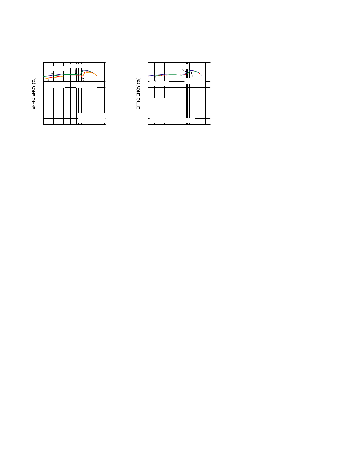
Micrel, Inc. MIC23250
Typical Characteristics (Continued)
Efficiency V
100
VIN = 2.7V
90
80
70
VIN = 4.2V
60
50
40
30
20
10
0
1 10 100 1000
= 1.575V
OUT
VIN = 3.0V
VIN = 3.6V
L = 1µH
C
OUT
LOAD (mA)
= 4.7µF
Dual Output Efficiency
100
90
80
70
VIN = 3.6V
60
50
40
V
V
30
Load1 = Load2
20
L1 = L2 = 1µH
10
C
0
1 10 100 1000
OUT1
OUT2
OUT1
VIN = 3.3V
= 1.575V
= 1.8V
= C
OUT2
LOAD (mA)
VIN = 4.2V
= 4.7µF
December 2007
5
M9999-121707-A
Page 6
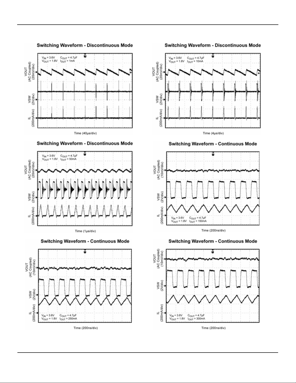
Micrel, Inc. MIC23250
Functional Characteristics
December 2007
6
M9999-121707-A
Page 7
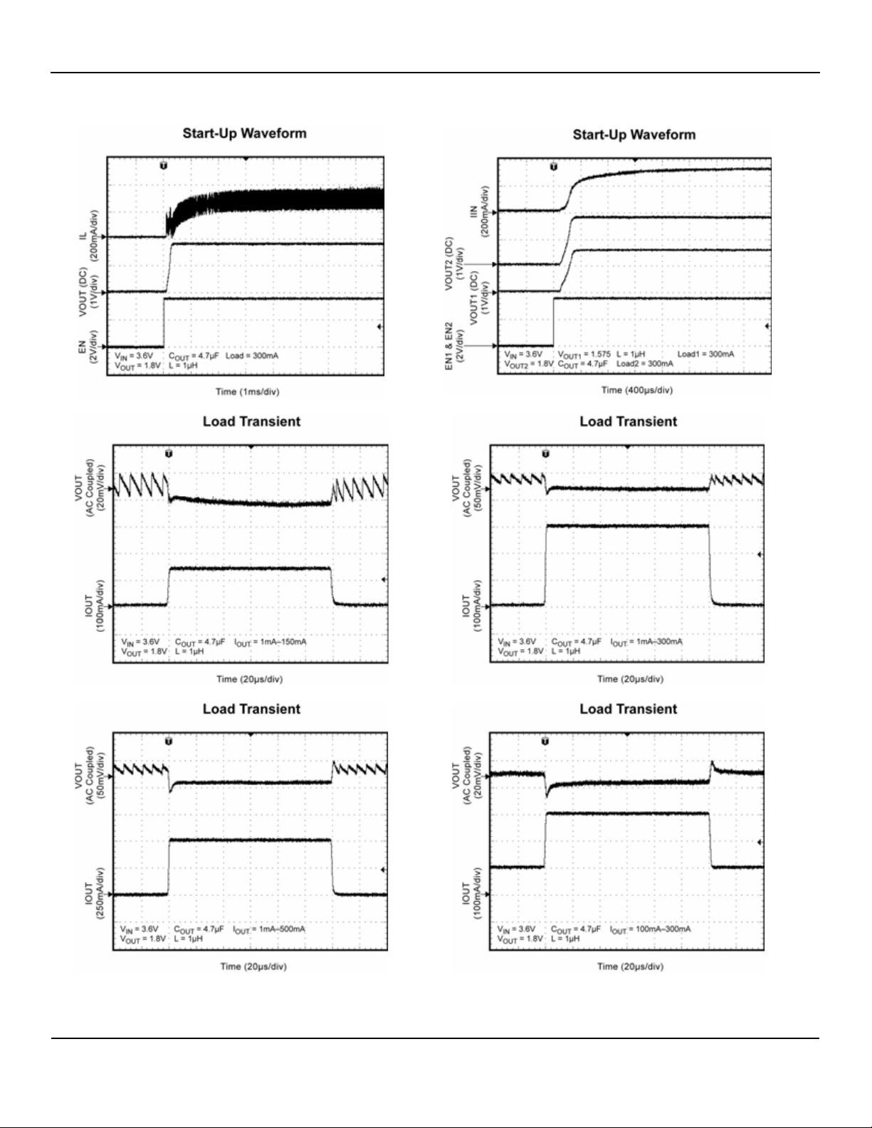
Micrel, Inc. MIC23250
Functional Characteristics (Continued)
December 2007
7
M9999-121707-A
Page 8
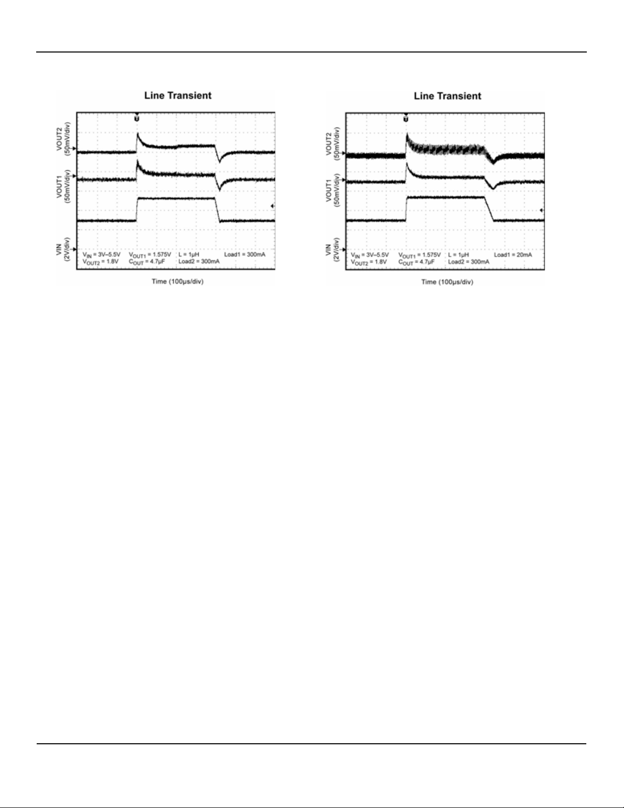
Micrel, Inc. MIC23250
Functional Characteristics (Continued)
December 2007
8
M9999-121707-A
Page 9
Micrel, Inc. MIC23250
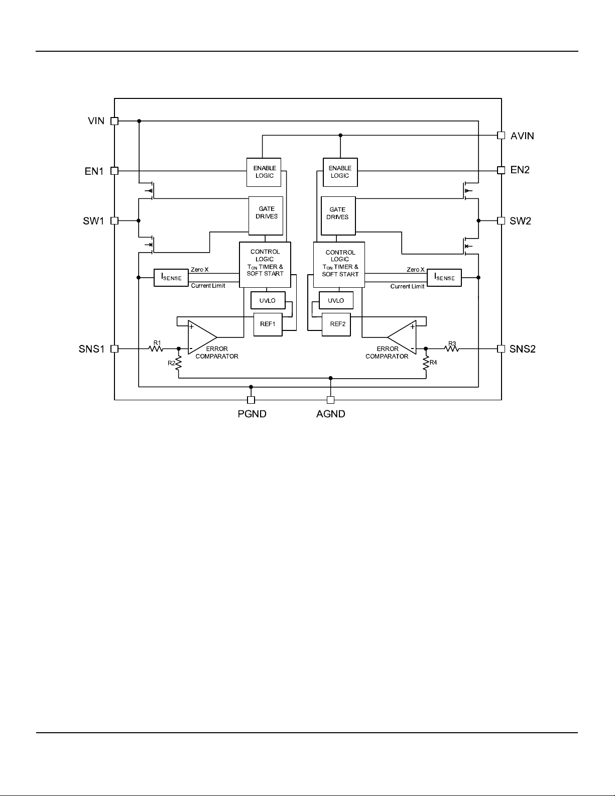
Functional Diagram
MIC23250 Simplified Block Diagram
December 2007
9
M9999-121707-A
Page 10

Micrel, Inc. MIC23250
Functional Description
VIN
The VIN provides power to the internal MOSFETs for the
switch mode regulator along with the current limit sensing.
The VIN operating range is 2.7V to 5.5V so an input
capacitor with a minimum of 6.3V voltage rating is
recommended. Due to the high switching speed, a
minimum of 2.2µF bypass capacitor placed close to VIN
and the power ground (PGND) pin is required. Based upon
size, performance and cost, a TDK C1608X5R0J476K,
size 0603, 4.7µF ceramic capacitor is highly recommended
for most applications. Refer to the layout
recommendations for details.
AVIN
The analog VIN (AVIN) provides power to the analog
supply circuitry. AVIN and VIN must be tied together.
Careful layout should be considered to ensure high
frequency switching noise caused by VIN is reduced
before reaching AVIN. A 0.01µF bypass capacitor placed
as close to AVIN as possible is recommended. See layout
recommendations for details.
EN1/EN2
The enable pins (EN1 and EN2) control the on and off
states of outputs 1 and 2, respectively. A logic high signal
on the enable pin activates the output voltage of the
device. A logic low signal on each enable pin deactivates
the output. MIC23250 features built-in soft-start circuitry
that reduces in-rush current and prevents the output
voltage from overshooting at start up.
SNS1/SNS2
The SNS pin (SNS1 or SNS2) is connected to the output
of the device to provide feedback to the control circuitry. A
minimum of 2.2µF bypass capacitor should be connected
in shunt with each output. Based upon size, performance
and cost, a TDK C1608X5R0J476K, size 0603, 4.7µF
ceramic capacitor is highly recommended for most
applications. In order to reduce parasitic inductance, it is
good practice to place the output bypass capacitor as
close to the inductor as possible. The SNS connection
should be placed close to the output bypass capacitor.
Refer to the layout recommendations for more details.
PGND
The power ground (PGND) is the ground path for the high
current in PWM mode. The current loop for the power
ground should be as small as possible and separate from
the Analog ground (AGND) loop. Refer to the layout
recommendations for more details.
AGND
The signal ground (AGND) is the ground path for the
biasing and control circuitry. The current loop for the signal
ground should be separate from the Power ground
(PGND) loop. Refer to the layout recommendations for
more details.
SW1/SW2
The switching pin (SW1 or SW2) connects directly to one
end of the inductor (L1 or L2) and provides the current
path during switching cycles. The other end of the inductor
is connected to the load and SNS pin. Due to the high
speed switching on this pin, the switch node should be
routed away from sensitive nodes.
December 2007
10
M9999-121707-A
Page 11

Micrel, Inc. MIC23250
Applications Information
given in two methods; permissible DC current and
saturation current. Permissible DC current can be rated
The MIC23250 is designed for high performance with a
small solution size. With a dual 400mA output inside a tiny
2mm x 2mm Thin MLF
®
package and requiring only six
external components, the MIC23250 meets today’s
miniature portable electronic device needs. While small
solution size is one of its advantages, the MIC23250 is big
either for a 40°C temperature rise or a 10% to 20% loss in
inductance. Ensure the inductor selected can handle the
maximum operating current. When saturation current is
specified, make sure that there is enough margin so that
the peak current of the inductor does not cause it to
saturate. Peak current can be calculated as follows:
in performance. Using the Hyper Light Load™ switching
scheme, the MIC23250 is able to maintain high efficiency
throughout the entire load range while providing ultra-fast
load transient response. Even with all the given benefits,
the MIC23250 can be as easy to use as linear regulators.
The following sections provide an over view of
implementing MIC23250 into related applications
Input Capacitor
A minimum of 2.2µF ceramic capacitor should be placed
close to the VIN pin and PGND pin for bypassing. A TDK
C1608X5R0J476K, size 0603, 4.7µF ceramic capacitor is
recommended based upon performance, size and cost. A
X5R or X7R temperature rating is recommended for the
input capacitor. Y5V temperature rating capacitors, aside
from losing most of their capacitance over temperature,
⎡
+=
⎢
VII
⎣
−
⎛
⎜
OUTOUTPEAK
⎜
⎝
××
2
As shown by the previous calculation, the peak inductor
current is inversely proportional to the switching frequency
and the inductance; the lower the switching frequency or
the inductance the higher the peak current. As input
voltage increases the peak current also increases.
The size of the inductor depends on the requirements of
the application. Refer to the Application Circuit and Bill of
Material for details.
DC resistance (DCR) is also important. While DCR is
inversely proportional to size, DCR can represent a
significant efficiency loss. Refer to the Efficiency
Considerations.
⎤
VV
/1
⎞
INOUT
⎟
⎥
⎟
Lf
⎠
⎦
can also become resistive at high frequencies. This
reduces their ability to filter out high frequency noise.
Output Capacitor
The MIC23250 was designed for use with a 2.2µF or
Compensation
The MIC23250 is designed to be stable with a 0.47µH to
4.7µH inductor with a minimum of 2.2µF ceramic (X5R)
output capacitor.
greater ceramic output capacitor. Increasing the output
capacitance will lower output ripple and improve load
transient response but could increase solution size or cost.
A low equivalent series resistance (ESR) ceramic output
capacitor such as the TDK C1608X5R0J476K, size 0603,
4.7µF ceramic capacitor is recommended based upon
performance, size and cost. Either the X7R or X5R
Efficiency Considerations
Efficiency is defined as the amount of useful output power,
divided by the amount of power supplied.
⎛
Efficiency
⎜
=
⎜
⎝
⎞
IV
×
OUTOUT
⎟
⎟
IV
×
ININ
⎠
100%_ ×
temperature rating capacitors are recommended. The Y5V
and Z5U temperature rating capacitors, aside from the
undesirable effect of their wide variation in capacitance
over temperature, become resistive at high frequencies.
Maintaining high efficiency serves two purposes. It
reduces power dissipation in the power supply, reducing
the need for heat sinks and thermal design considerations
and it reduces consumption of current for battery powered
Inductor Selection
Inductor selection will be determined by the following (not
necessarily in the order of importance);
• Inductance
• Rated current value
• Size requirements
• DC resistance (DCR)
The MIC23250 was designed for use with an inductance
range from 0.47µH to 4.7µH. Typically, a 1µH inductor is
recommended for a balance of transient response,
efficiency and output ripple. For faster transient response a
0.47µH inductor may be used. For lower output ripple, a
4.7µH is recommended.
applications. Reduced current draw from a battery
increases the devices operating time and is critical in hand
held devices.
There are two types of losses in switching converters; DC
losses and switching losses. DC losses are simply the
power dissipation of I
2
R. Power is dissipated in the high
side switch during the on cycle. Power loss is equal to the
high side MOSFET R
multiplied by the Switch Current
DSON
squared. During the off cycle, the low side N-channel
MOSFET conducts, also dissipating power. Device
operating current also reduces efficiency. The product of
the quiescent (operating) current and the supply voltage is
another DC loss. The current required driving the gates on
and off at a constant 4MHz frequency and the switching
transitions make up the switching losses.
Maximum current ratings of the inductor are generally
December 2007
11
M9999-121707-A
Page 12
Micrel, Inc. MIC23250
Efficiency V
100
VIN = 2.7V
80
60
VIN = 3.3V
40
20
0
0.1 1 10 100 1000
LOAD (mA)
= 1.8V
OUT
VIN = 3.6V
V
= 1.8V
OUT
L = 1µH
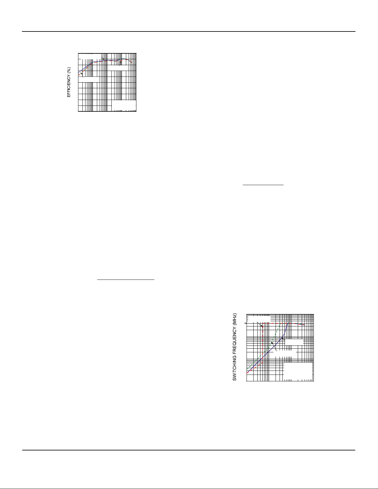
The Figure above shows an efficiency curve. From no load
to 100mA, efficiency losses are dominated by quiescent
current losses, gate drive and transition losses. By using
the Hyper Light Load™ mode the MIC23250 is able to
maintain high efficiency at low output currents.
Over 100mA, efficiency loss is dominated by MOSFET
and inductor losses. Higher input supply voltages
R
DSON
will increase the Gate-to-Source threshold on the internal
MOSFETs, thereby reducing the internal R
DSON
. This
improves efficiency by reducing DC losses in the device.
All but the inductor losses are inherent to the device. In
which case, inductor selection becomes increasingly
critical in efficiency calculations. As the inductors are
reduced in size, the DC resistance (DCR) can become
quite significant. The DCR losses can be calculated as
follows:
2
L_Pd = I
OUT
× DCR
From that, the loss in efficiency due to inductor resistance
can be calculated as follows:
⎡
⎛
LossEfficiency
⎜
1_ ×
−=
⎢
⎜
⎢
⎝
⎣
IV
×
OUTOUT
+×
⎤
⎞
⎟
100
⎥
⎟
PLIV
_
⎥
DOUTOUT
⎠
⎦
Efficiency loss due to DCR is minimal at light loads and
gains significance as the load is increased. Inductor
selection becomes a trade-off between efficiency and size
in this case.
Hyper Light Load Mode™
The MIC23250 uses a minimum on and off time
proprietary control loop (patented by Micrel). When the
output voltage falls below the regulation threshold, the
error comparator begins a switching cycle that turns the
PMOS on and keeps it on for the duration of the minimumon-time. This increases the output voltage. If the output
voltage is over the regulation threshold, then the error
comparator turns the PMOS off for a minimum-off-time
until the output drops below the threshold. The NMOS acts
as an ideal rectifier that conducts when the PMOS is off.
Using a NMOS switch instead of a diode allows for lower
voltage drop across the switching device when it is on. The
asynchronous switching combination between the PMOS
and the NMOS allows the control loop to work in
discontinuous mode for light load operations. In
discontinuous mode, the MIC23250 works in pulse
frequency modulation (PFM) to regulate the output. As the
output current increases, the off-time decreases, thus
providing more energy to the output. This switching
scheme improves the efficiency of MIC23250 during light
load currents by only switching when it is needed. As the
load current increases, the MIC23250 goes into
continuous conduction mode (CCM) and switches at a
frequency centered at 4MHz. The equation to calculate the
load when the MIC23250 goes into continuous conduction
mode may be approximated by the following formula:
×−
DVV
I
LOAD
⎜
⎝
⎛
⎜
=
OUTIN
2
×
⎞
⎟
⎟
fL
⎠
As shown in the previous equation, the load at which
MIC23250 transitions from Hyper Light Load™ mode to
PWM mode is a function of the input voltage (V
voltage (V
), duty cycle (D), inductance (L) and
OUT
), output
IN
frequency (f). This is illustrated in the graph below. Since
the inductance range of MIC23250 is from 0.47µH to
4.7µH, the device may then be tailored to enter Hyper
Light Load™ mode or PWM mode at a specific load
current by selecting the appropriate inductance. For
example, in the graph below, when the inductance is
4.7µH the MIC23250 will transition into PWM mode at a
load of approximately 4mA. Under the same condition,
when the inductance is 1µH, the MIC23250 will transition
into PWM mode at approximately 70mA.
Switching Frequency
vs. Output Current
10
L = 4.7µH
4MHz
1
0.1
0.01
1 10 100 1000
OUTPUT CURRENT (mA)
L = 1µH
L = 2.2µH
VIN = 3.6V
V
OUT
C
OUT
= 1.8V
= 4.7µF
December 2007
12
M9999-121707-A
Page 13
Micrel, Inc. MIC23250
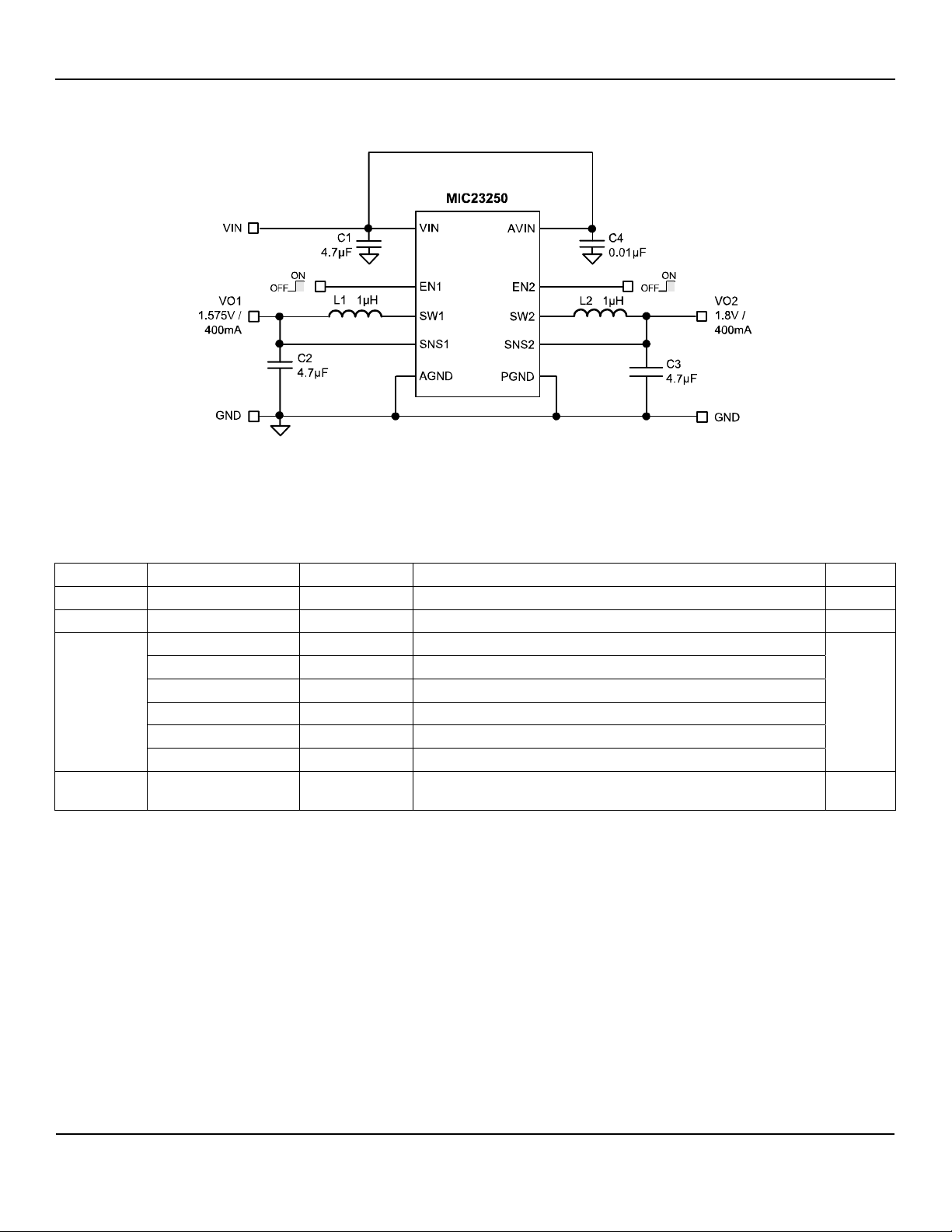
MIC23250 Typical Application Circuit (Fixed 1.575V, 1.8V)
Bill of Materials
Item Part Number Manufacturer Description Qty
C1, C2, C3 C1608X5R0J476K TDK
C4 VJ0603Y103KXXAT Vishay
LQM21PN1R0M00 Murata
LQH32CNR1R0M33 Murata
L1, L2
LQM31P1R0M00 Murata
GFL251812T TDK
LQM31PNR47M00 Murata
MIPF2520D1R5 FDK
U1 MIC23250-GFHYMT Micrel, Inc.
Notes:
1. TDK: www.tdk.com
2. Vishay: www.vishay.com
3. Murata: www.murata.com
4. FDK: www.fdk.co.jp
5. Micrel, Inc: www.micrel.com
(1)
4.7µF Ceramic Capacitor, 6.3V, X5R, Size 0603 3
(2)
0.01µF Ceramic Capacitor, 25V, X7R, Size 0603 1
(3)
1µH, 0.8A, 190m, L2mm x W1.25mm x H0.5mm
(3)
1µH, 1A, 60m, L3.2mm x W2.5mm x H2.0mm
(3)
1µH, 1.2A, 120m, L3.2mm x W1.6mm x H0.95mm
(1)
1µH, 0.8A, 100m, L2.5mm x W1.8mm x H1.35mm
(3)
0.47µH, 1.4A, 80m, L3.2mm x W1.6mm x H0.85mm
(4)
1.5µH, 1.5A, 70m, L2.5mm x W2mm x H1.0mm
(5)
4MHz Dual 400mA Buck Regulator
with Hyper Light Load™ Mode
2
1
December 2007
13
M9999-121707-A
Page 14
Micrel, Inc. MIC23250
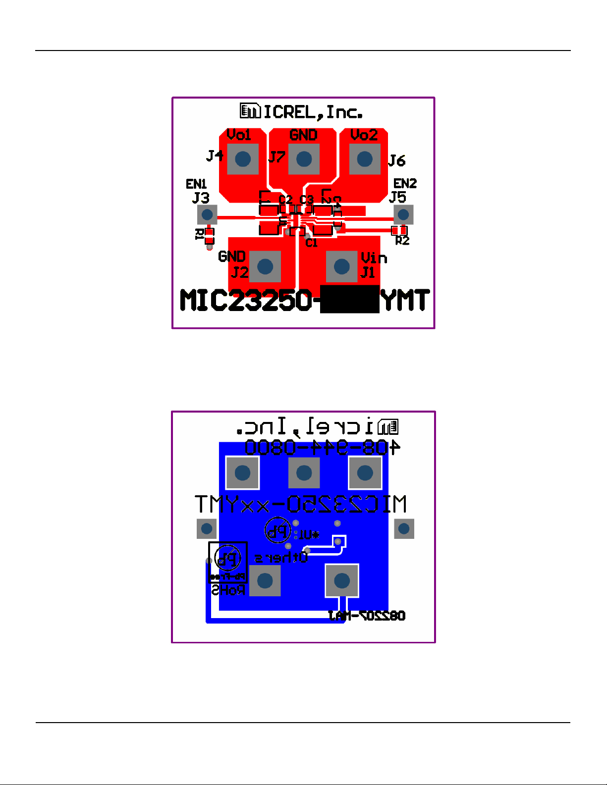
PCB Layout Recommendations
Top Layer
December 2007
Bottom Layer
14
M9999-121707-A
Page 15
Micrel, Inc. MIC23250
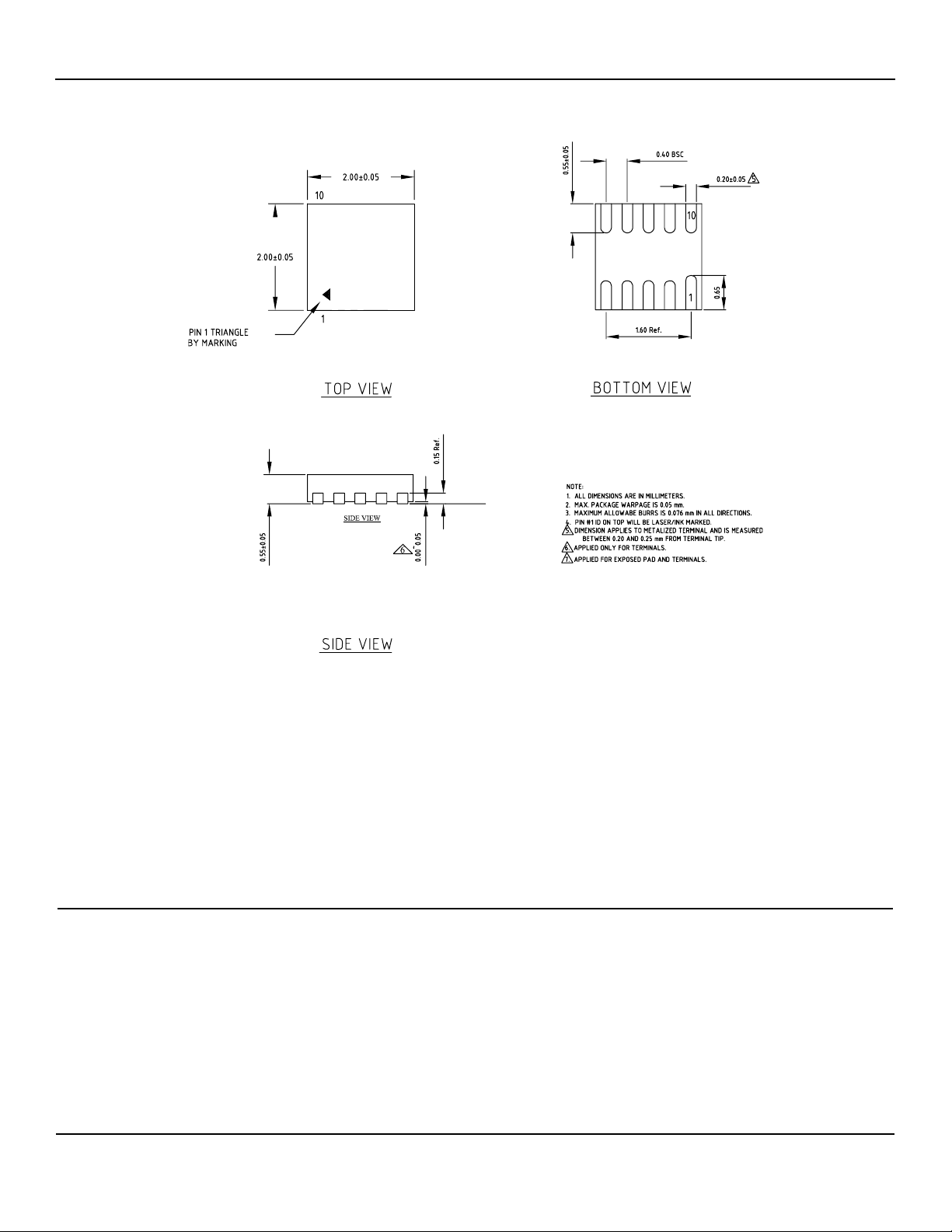
Package Information
10-Pin 2mm x 2mm Thin MLF® (MT)
MICREL, INC. 2180 FORTUNE DRIVE SAN JOSE, CA 95131 USA
TEL +1 (408) 944-0800 FAX +1 (408) 474-1000 WEB http://www.micrel.com
The information furnished by Micrel in this data sheet is believed to be accurate and reliable. However, no responsibility is assumed by Micrel for its
Micrel Products are not designed or authorized for use as components in life support appliances, devices or systems where malfunction of a product
can reasonably be expected to result in personal injury. Life support devices or systems are devices or systems that (a) are intended for surgical implant
into the body or (b) support or sustain life, and whose failure to perform can be reasonably expected to result in a significant injury to the user. A
Purchaser’s use or sale of Micrel Products for use in life support appliances, devices or systems is a Purchaser’s own risk and Purchaser agrees to fully
December 2007
use. Micrel reserves the right to change circuitry and specifications at any time without notification to the customer.
indemnify Micrel for any damages resulting from such use or sale.
© 2007 Micrel, Incorporated.
15
M9999-121707-A
 Loading...