

Page 1
MIC2185 Micrel
MIC2185
Low Voltage Synchronous Boost PWM Control IC
Final Information
General Description
Micrel’s MIC2185 is a high efficiency synchronous boost
PWM control IC. With its wide input voltage range of 2.9V to
14V, the MIC2185 can be used to efficiently boost voltages in
1- or 2-cell Li Ion battery powered applications, as well as
fixed 3.3V and 5V systems. Its powerful 5Ω output drivers
allow the MIC2185 to supply large output currents with the
selection of the proper external MOSFETs.
With it’s fixed frequency PWM architecture, and easily synchronized drive, the MIC2185 is ideal for noise-sensitive
telecommunications applications. The nominal 400kHz operating frequency of the MIC2185 can be divided by two,
allowing the device to be externally synchronized to frequencies below 400kHz.
The MIC2185 also features a low current shutdown mode and
a programmable undervoltage lockout. A skipped pulse mode
of operation can be manually set to achieve higher efficiencies at light load conditions.
The MIC2185 is available in a 16 pin SOIC package and 16
pin QSOP package with an ambient temperature operating
range from –40°C to 85°C.
Ordering Information
Part Number Frequency Voltage Junction Temp. Range Package
MIC2185BM 200/400kHz Adj –40°C to +125°C 16-lead SOP
MIC2185BQS 200/400kHz Adj –40°C to +125°C 16-lead QSOP
Features
• Input voltage range: 2.9V to 14V
• 95% efficiency
• Oscillator frequency of 200kHz/400kHz
• Frequency sync to 600kHz
• 0.5µA shutdown current
• Two 5Ω output drivers
• Front edge blanking
• PWM Current Mode Control
• Cycle-by-Cycle current limiting
• Frequency foldback protection
• Adjustable under-voltage lockout
• Precision 1.245V reference output
• 16 pin SOIC narrow body package
Applications
• 3.3V to 5V conversion in telecom systems
• Satellite Phones
• Cable Modems
• 1-and 2-cell Li Ion battery operated equipment
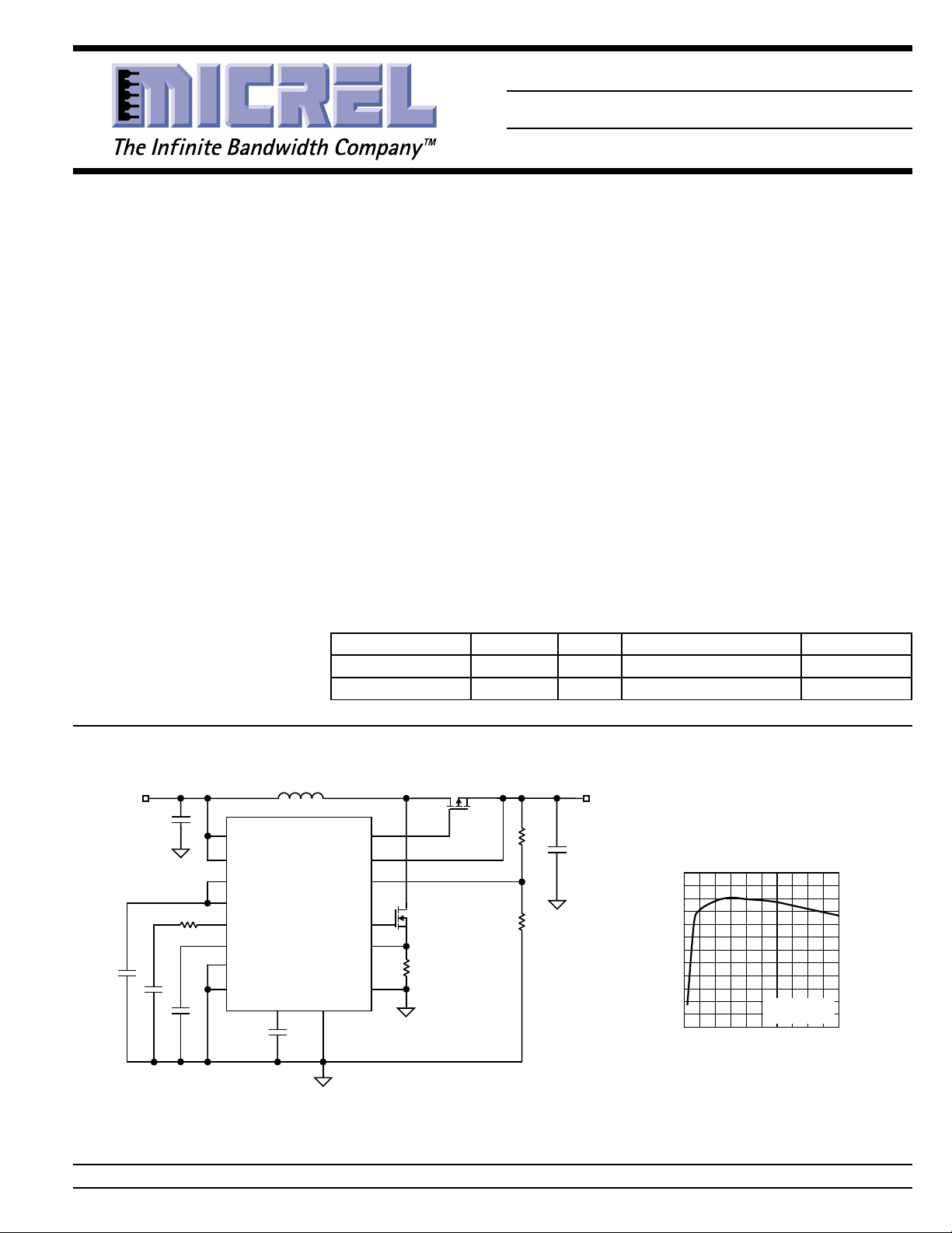
T ypical Application
VIN = 3.3V
C
IN
1
VINA
7
EN/UVLO
15
FREQ/2
10
VDD
4
COMP
8
VREF
11
SYNC
2
SKIP
2.4µH
MIC2185
SS
3
SGND
5
OUTP
VINP
FB
OUTN
CSH
PGND
14
16
6
13
9
12
Si9803DY (x2)
Si4884DY (x2)
8mΩ
Adjustable Output Synchronous Boost Converter
Micrel, Inc. • 1849 Fortune Drive • San Jose, CA 95131 • USA • tel + 1 (408) 944-0800 • fax + 1 (408) 944-0970 • http://www.micrel.com
December 2002 1 MIC2185
V
= 5V
OUT
C
OUT
5V Output Efficiency
100
95
90
85
80
EFFICIENCY (%)
75
70
012345
OUTPUT CURRENT (A)
VIN = 3.3V
200kHz PWM
Page 2
MIC2185 Micrel
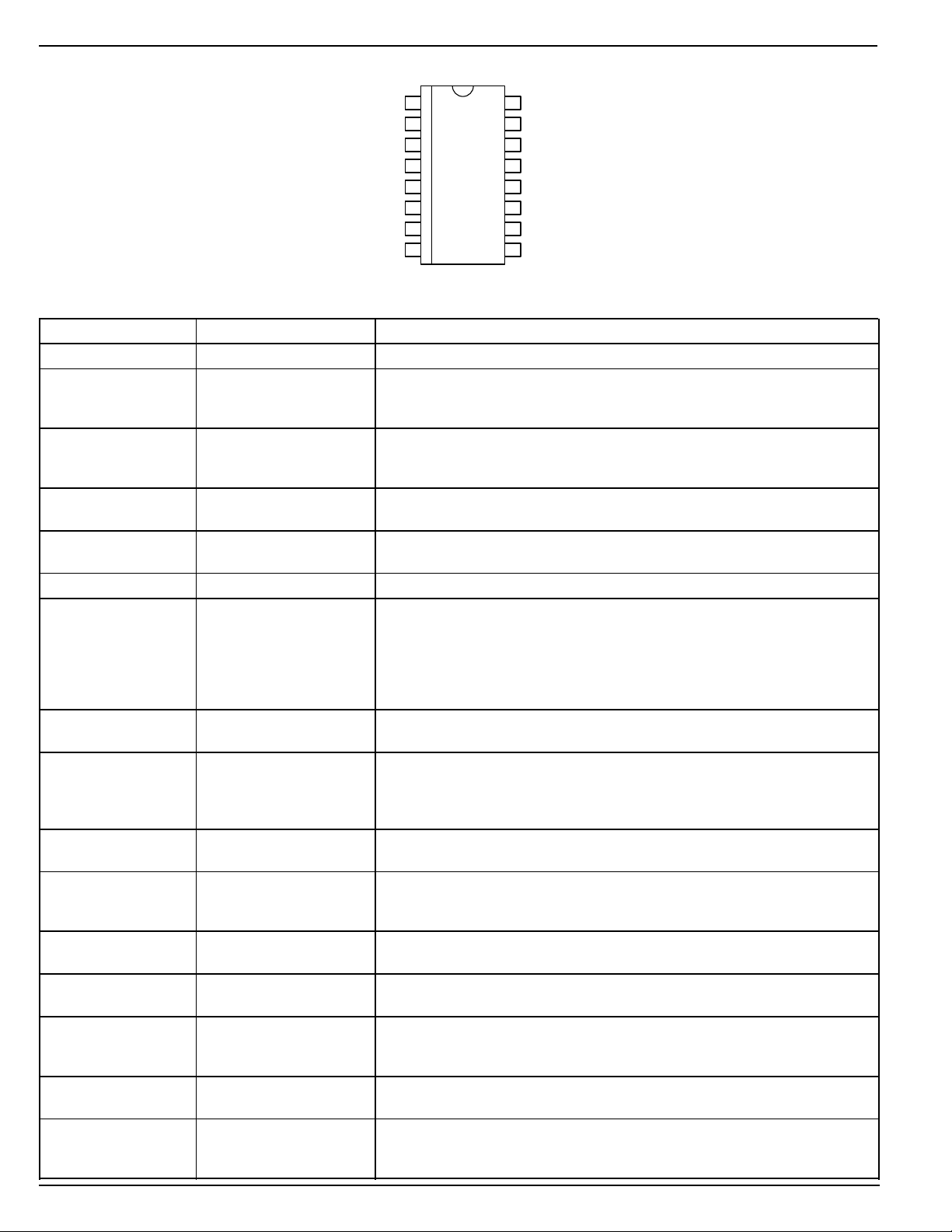
Pin Configuration
SKIP
COMP
SGND
EN/UVLO
VREF
16-pin Narrow Body SOP (M)
Pin Description
Pin Number Pin Name Pin Function
1 VINA Input voltage to control circuitry (2.9V to 14V).
2 SKIP Skip (Input): Regulator operates in PWM mode (no pulse skipping) when pin
3 SS Soft Start (External Component) : Reduces the inrush current and delays
4 COMP Compensation (Output): Internal error amplifier output. Connect to a
5 SGND Small Signal Ground (Return) : Must be routed separately from other
6 FB Feedback (Input) : Regulates FB to 1.245V.
7 EN/UVLO Enable/Undervoltaqe Lockout (Input): A low level on this pin will power down
8 VREF Voltage Reference (Output) : The 1.245V reference is available on this pin.
9 CSH Current Sense (Input) : The (+) input to the current limit comparator. A built
10 VDD 3V Internal Linear-Regulator (Output) : VDD is also the supply voltage bus
11 SYNC Frequency Synchronization (Input): Connect an external clock signal to
12 PGND MOSFET Driver Power Ground (Return) : Connects bottom of current sense
13 OUTN N-Channel Drive (Output) : High current drive for n-channel MOSFET.
14 OUTP P-Channel Drive (Output) : High current drive for the synchronous p-channel
15 FREQ/2 Frequency Divider (Input) : When this pin is low, the oscillator frequency is
16 VINP Gate Drive Voltage (Input) : This is the power input to the gate drive circuitry
SS
FB
1VINA
2
3
4
5
6
7
8
16 VINP
FREQ/2
15
OUTP
14
OUTN
13
PGND
12
SYNC
11
VDD
10
CSH
9
16-pin QSOP (QS)
is pulled low, and skip mode when raised to VDD. There is no automatic
switching between PWM and skip mode available on this device.
and slows the output voltage rise time. A 5µA current source will charge the
capacitor up to VDD.
capacitor or series RC network to compensate the regulator’s control loop.
grounds to the (–) terminal of C
the device, reducing the quiescent current to under 0.5µA. This pin has two
separate thresholds, below 1.5V (typical) the output switching is disabled,
and below 0.9V (typical) the device is forced into a complete micropower
shutdown. The 1.5V threshold functions as an accurate undervoltage lockout
(UVLO) with 140mV hysteresis.
A 0.1µF capacitor should be connected form this pin to SGnd.
in offset of 100mV (typical) between CSH and SGnd in conjunction with the
current sense resistor sets the current limit threshold level. This is also the
(+) input to the current amplifier.
for the chip. Bypass to SGND with 1µF. Maximum source current is 0.5mA.
synchronize the oscillator. Leading edge of signal above 1.4V (typical) starts
switching cycle. Connect to SGND if not used.
resistor and the (–) terminal of CIN.
Voltage swing is from ground to VINP. On-resistance is typically 5Ω.
MOSFET. Voltage swing is from ground to VINP. On-resistance is typically
5Ω.
400KHz. When this pin is raised to VDD, the oscillator frequency is 200KHz.
(2.9V to 14V). This pin is typically connected to the output voltage to
enhance gate drive.
OUT
.
MIC2185 2 December 2002
Page 3
MIC2185 Micrel
Absolute Maximum Ratings (Note 1)
Supply Voltage (VINA, VINP) .........................................15V
Digital Supply Voltage (V
Skip Pin Voltage (V
SKIP
Comp Pin Voltage (V
Feedback Pin Voltage (V
Enable Pin Voltage (V
Current Sense Voltage (V
Sync Pin Voltage (V
SYNC
Freq/2 Pin Voltage (V
) ...........................................7V
DD
) .................................. –0.3V to 7V
).............................. –0.3V to 3V
COMP
) ............................ –0.3V to 3V
FB
EN/UVLO
) ..................... –0.3V to 15V
)......................... –0.3V to 1V
CSH
) ................................ –0.3V to 7V
) ........................... –0.3V to 7V
FREQ/2
Operating Ratings (Note 2)
Supply Voltage (V
Operating Ambient Temperature.........–40°C ≤ T
Junction Temperature ....................... –40°C ≤ T
PackageThermal Resistance
16-lead SOP ...............................................100°C/W
θ
JA
θJA 16-lead QSOP.............................................163°C/W
ESD Rating, Note 3
A, VINP) ........................ +2.9V to +14V
IN
≤ +85°C
A
≤ +125°C
J
Power Dissipation (PD)
16 lead SOP..................................400mW @ TA = 85°C
16 lead QSOP ................................ 245mW@ TA = 85°C
Ambient Storage Temp ............................–65°C to +150°C
Electrical Characteristics
VINA= 5V, VinP= V
indicate –40°C < TJ < +125°C.
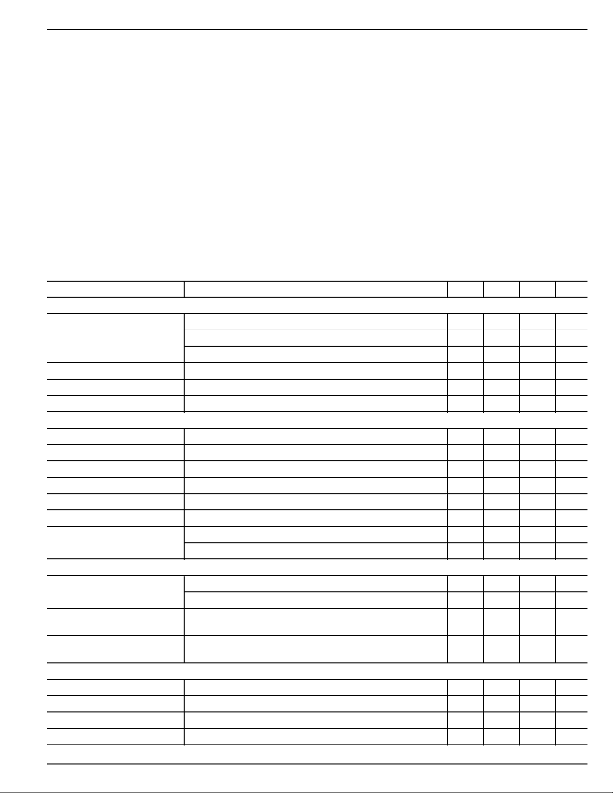
Parameter Condition Min Typ Max Units
Regulation
Feedback Voltage Reference (±1%) 1.233 1.245 1.258 V
Feedback Bias Current 50 nA
Output Voltage Line Regulation 3V ≤ VINA ≤ 9V +0.08 % / V
Output Voltage Load Regulation 0mV ≤ CSH ≤ 75mV –1.2 %
Input & VDD Supply
VINA Input Current, PWM mode V
VINP Input Current, PWM mode V
VINA Input Current, SKIP mode V
Shutdown Quiescent Current V
Digital Supply Voltage (VDD) IL = 0 2.8 3.0 3.2 V
Digital Supply Load Regulation IL = 0 to 0.5mA 0.03 V
Undervoltage Lockout VDD upper threshold (turn on threshold) 2.9 2.75 V
Reference Output (V
Reference Voltage (±1.5%) 1.226 1.245 1.264 V
Reference Voltage Line 5V < VinA < 9V 2 mV
Regulation
Reference Voltage Load 0 < I
Regulation
Enable/UVLO
Enable Input Threshold 0.6 0.9 1.2 V
UVLO Threshold 1.4 1.5 1.6 V
UVLO Hysteresis 140 mV
Enable Input Current V
OUT
=12V, V
)
REF
EN/UVLO
= 5V, V
(±2%) 1.220 1.270 V
3V ≤ VINA ≤ 9V; 0mV ≤ CSH ≤ 75mV; (±3%) 1.208 1.245 1.282 V
= 0V 0.8 mA
SKIP
= 0V (excluding external MOSFET gate current) 3.8 mA
SKIP
= 5V 0.6 mA
SKIP
EN/UVLO
VDD lower threshold (turn off threshold) 2.65 V
(±2.5%) 1.213 1.276 V
REF
EN/UVLO
= 0V, V
SKIP
= 0V; (I
< 100µA1mV
= 5V 0.2 5 µA
VINA
+ I
= 0V, V
FREQ/2
) 0.5 µA
VINP
= 0V, TJ = 25°C, unless otherwise specified. Bold values
CSH
December 2002 3 MIC2185
Page 4
MIC2185 Micrel
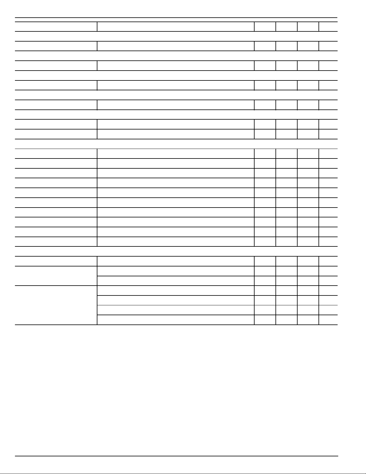
Parameter Condition Min Typ Max Unit
Soft Start
Soft Start Current 5 µA
Current Limit
Current Limit Threshold Voltage Voltage on CSH to trip current limit 100 mV
Error Amplifier
Error Amplifier Gain 20 V/V
Current Amplifier
Current Amplifier Gain 3.7 V/V
SKIP Input
SKIP Threshold 0.6 1.4 2.2 V
SKIP Input Current V
Oscillator Section
Oscillator Frequency (fS) 360 400 440 kHz
Maximum Duty Cycle VFB = 1.0V 85 %
Minimum On Time VFB = 1.5V 180 ns
FREQ/2 frequency (fS)V
Frequency Foldback Threshold Measured at FB pin 0.3 V
Frequency Foldback Frequency V
SYNC Threshold Level 0.6 1.4 2.2 V
SYNC Input Current 0.1 5 µA
SYNC Minimum Pulse Width 200 ns
SYNC Capture Range Note 4 fO+15 % 600 kHz
Gate Drivers (OUTN and OUTP)
Rise/Fall Time CL = 3300pF 50 ns
Driver Non-overlap Time VINP = 12V 70 ns
Output Driver Impedance Source; VINP = 12V 4 8 Ω
= 3V 0.1 5 µA
SKIP
=3V 170 200 230
FREQ/2
=0V 90 kHz
FREQ/2
VINP = 5V 90 ns
Sink; VINP = 12V 3 7 Ω
Source; VINP = 5V 5 11 Ω
Sink; VINP = 5V 5 11 Ω
Note 1. Absolute maximum ratings indicate limits beyond which damage to the component December occur. Electrical specifications do not apply
Note 2. The device is not guaranteed to function outside its operating rating.
Note 3. Devices are ESD sensitive. Handling precautions recommended.
Note 4. See application information for limitations on maximum operating frequency.
when operating the device outside of its operating ratings. The maximum allowable power dissipation is a function of the maximum junction
temperature, T
, the junction-to-ambient thermal resistance, θJA, and the ambient temperature, TA.
J(max)
MIC2185 4 December 2002
Page 5
MIC2185 Micrel
0
0.5
1
1.5
2
2.5
3
3.5
4
4.5
5
0 2 4 6 8 10 12 14 16
I
Q
(mA)
INPUT VOLTAGE (V
INA
)
Quiescent Current vs.
Input Voltage(PWM Mode)
400kHz
200kHz
VINP =12V
DC
IQ = I
QVINA+IQVINP
g
g
1.245
1.2455
1.246
1.2465
1.247
1.2475
0 2 4 6 8 10 12 14 16
REFERENCE VOLTAGE (V)
INPUT VOLTAGE (V
INA
)
Reference Voltage
vs. Input Voltage
VINP = 12V
DC
2.80
2.85
2.90
2.95
3.00
3.05
3.10
3.15
02468101214
VDD (V)
INPUT VOLTAGE (V
INA
)
VDD vs.
Input Voltage
VINP = 12V
DC
0
50
100
150
200
250
300
02468101214
I
ENABLE
(µA)
V
ENABLE
(V)
I
ENABLE
vs. V
ENABLE
VINP = 12V
DC
VINA = 5V
DC
85°C
–40°C
20°C
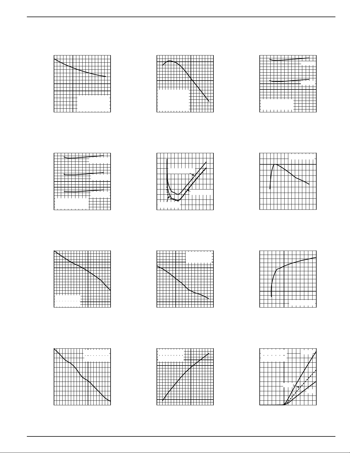
Typical Characteristics
Quiescent Current vs.
Temperature (SKIP Mode)
0.8
0.7
0.6
0.5
(mA)
0.4
0.3
Q(SKIP)
I
0.2
0.1
0
-40 -20 0 20 40 60 80 100120140
Quiescent Current vs.
Input Volta
VINA = 5V
DC
VINP = 12V
IQ = I
QVINA+IQVINP
TEMPERATURE (°C)
e (PWM Mode)
DC
5
4.5
VINP = 12V
4
3.5
3
(mA)
2.5
2
Q(PWM)
I
1.5
1
IQ = I
0.5
fS = 400kHz
0
0 2 4 6 8 10 12 14 16
+ I
QVINA
INPUT VOLTAGE (V
VINP = 9V
VINP = 5V
QVINP
INA
Quiescent Current vs.
Temperature (PWM Mode)
4.75
4.70
4.65
4.60
4.55
(mA)
4.50
VINA = 5V
Q(PWM)
I
4.45
4.40
4.35
4.30
Input Volta
DC
VINP = 12V
fS = 400kHz
IQ = I
-60
DC
QVINA+IQVINP
0
204060
-40
-20
TEMPERATURE (°C)
Quiescent Current vs.
e (SKIP Mode)
80
100
120
140
0.8
0.75
VINP = 12V
DC
0.7
(mA)
Q
I
0.65
VINP = 9V
DC
0.6
VINP = 5V
0.55
)
0 2 4 6 8 10 12 14 16
DC
INPUT VOLTAGE (V
INA
)
1.2470
1.2469
1.2468
1.2467
1.2466
1.2465
1.2464
1.2463
1.2462
1.2461
REFERENCE VOLTAGE (V)
1.2460
3.040
3.035
3.030
3.025
VDD (V)
3.020
3.015
3.010
December 2002 5 MIC2185
Reference Voltage
vs. Reference Current
VINP = 12V
VINA = 5V
0 102030405060708090100
0 0.10.20.30.40.50.60.70.80.91.0
DC
DC
REFERENCE CURRENT (µA)
VDD vs.
Load Current
VINP = 12V
VINA = 5V
I
(mA)
VDD
DC
DC
Reference Voltage
1.257
1.255
1.253
vs. Temperature
VINP = 12V
VINA = 5V
1.251
1.249
1.247
1.245
1.243
1.241
1.239
REFERENCE VOLTAGE (V)
1.237
-40 -20 0 20 40 60 80 100120140
TEMPERATURE (°C)
VDD vs.
3.08
3.07
3.06
Temperature
VINP = 12V
VINA = 5V
DC
DC
3.05
3.04
3.03
3.02
VDD (V)
3.01
3.00
2.99
2.98
0
-60
204060
-40
-20
TEMPERATURE (°C)
DC
DC
80
100
120
140
Page 6
MIC2185 Micrel
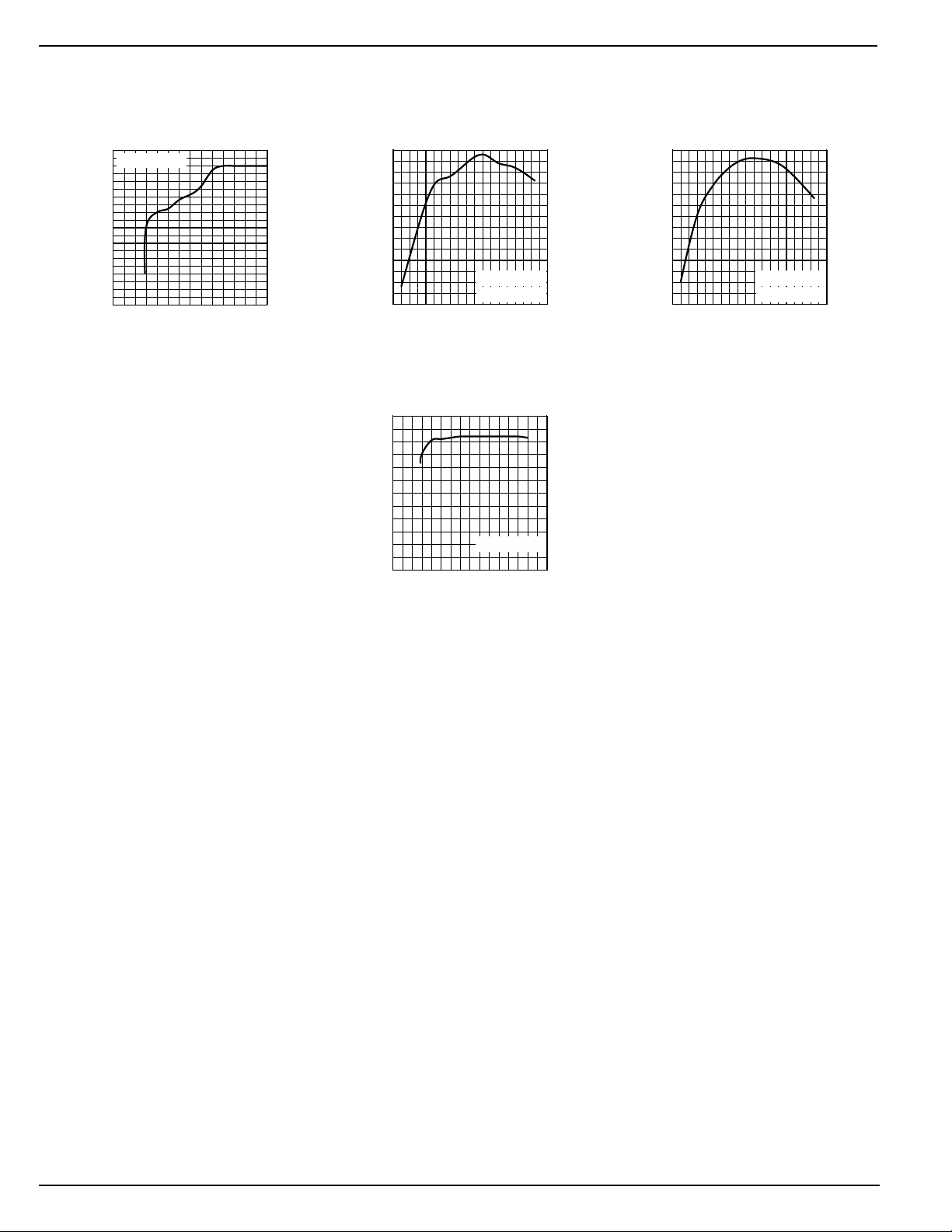
Oscillator Frequency
vs. Input Voltage
422
VINP = 12V
421
420
419
418
417
416
415
414
413
412
OSCILLATOR FREQUENCY (kHz)
02468101214
DC
INPUT VOLTAGE (V
INA
Oscillator Frequency
425
420
415
410
405
400
395
390
OSCILLATOR FREQUENCY (kHz)
)
120
100
OVERCURRENT THRESHOLD (mV)
vs. Temperature
VINP = 12V
VINA = 5V
-50
80
60
40
20
0
0 2 4 6 8 10 12 14 16
1030507090
-30
-10
TEMPERATURE (°C)
Overcurrent Threshold
vs. VINA
VINP = 12V
VINA (V)
DC
DC
110
DC
130
5.15
5.10
5.05
5.00
4.95
4.90
4.85
SOFT START CURRENT (µA)
4.80
Soft Start Current
vs. Temperature
-50
1030507090
-30
-10
TEMPERATURE (°C)
VINP = 12V
VINA = 5V
DC
DC
110
130
MIC2185 6 December 2002
Page 7
MIC2185 Micrel
Functional Diagram
V
IN
C
IN
L1
D1
Q2
V
OUT
C
OUT
EN/UVLO
SKIP
C
DECOUP
A
V
IN
1
VINP
GND
16
OUTP
14
V
7
2
fs/4
Control
Overcurrent Reset
Bias
On
REF
V
DD
P
FREQ/2
SYNC
SS
COMP
VREF
VDD
GND
OUTN
13
CSH
9
PGND
12
FB
6
15
Osc
11
3
4
8
10
Correction
Ramp
V
REF
V
Reset
P
PWM
Comparator
Gain = 3.7
Error
Amplifier
gm = 0.0002
Gain = 20
100k
DD
SGND
V
REF
fs/4
S
GND
5
Overcurrent
Comparator
Frequency
Foldback
0.1V
0.3V
P
GND
Q1
R
SENSE
R1
R2
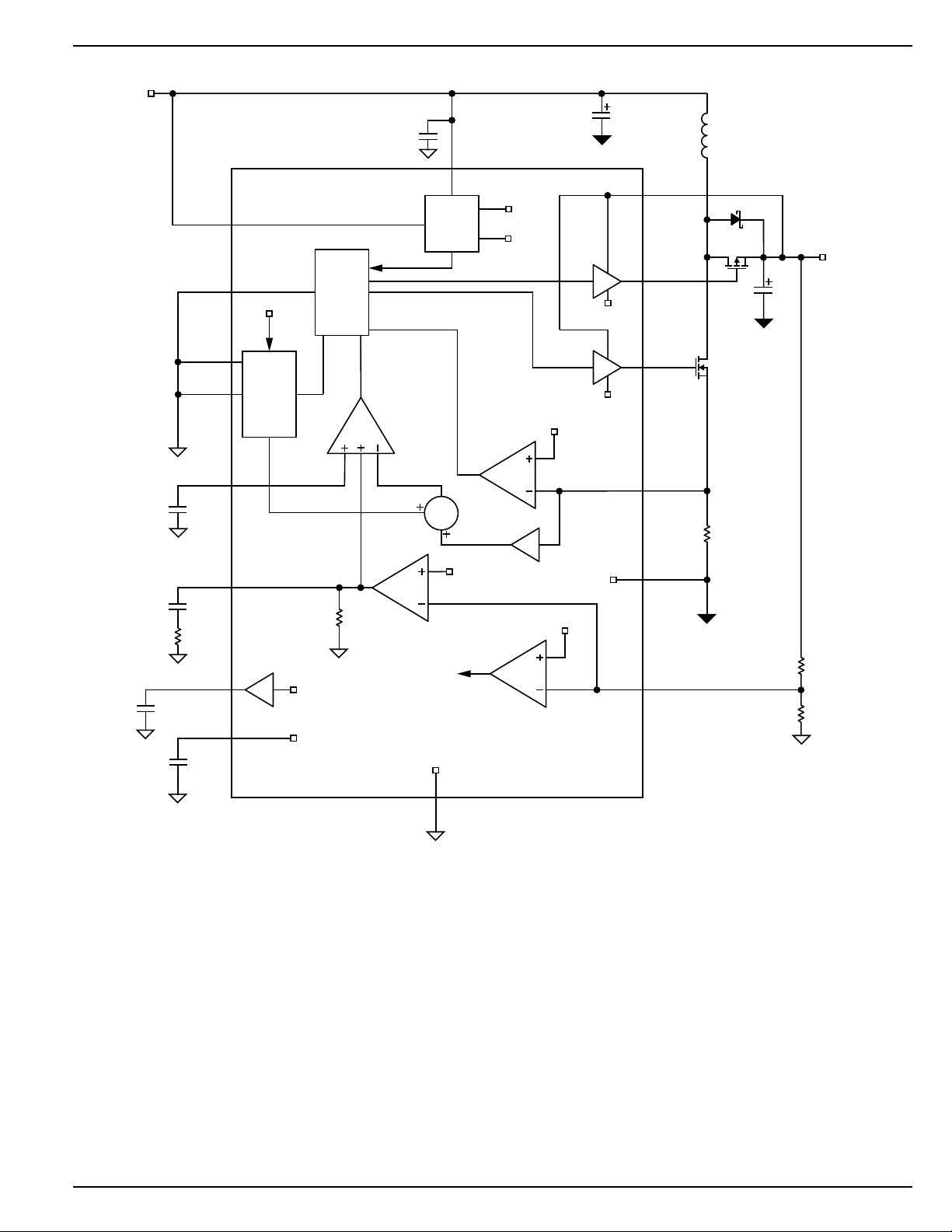
Figure 1. MIC2185 PWM Mode Block Diagram
Functional Description
The MIC2185 is a BiCMOS, switched mode, synchronous
boost (step up) control IC. The synchronous switched, high
side P-channel MOSFET, Q2, placed in parallel with the
output diode, D1, improves the efficiency of the boost converter. The lower voltage drop across the MOSFET reduces
power dissipation and increases efficiency. Current mode
control is used to achieve superior transient line and load
regulation. An internal corrective ramp provides slope compensation for stable operation above a 50% duty cycle. The
controller is optimized for high efficiency, high performance
DC-DC converter applications.
Figure 1 is a block diagram of the MIC2185 configured as a
PWM synchronous boost converter. The switching cycle
starts when OutN goes high and turns on the low side, Nchannel MOSFET, Q1. The Vgs of the MOSFET is equal to
VinP. This forces current to ramp up in the inductor. The
inductor current flows through the current sense resistor,
Rsense. The voltage across the resistor is amplified and
combined with an internal ramp for stability. This signal is
compared with the comp output signal of the error amplifier.
When the current signal equals the error voltage signal, the
low side MOSFET is turned off. The inductor current then
flows through the diode, D1, to the output. A delay between
the turn-off of the low side MOSFET and the turn-on of the
high side MOSFET prevents both MOSFETs from being on
at the same time, which would short the output to ground. At
the end of the non-overlap time, OutP pulls the gate of the
MOSFET to ground, turning on the high side, P-channel
December 2002 7 MIC2185
Page 8
MIC2185 Micrel
MOSFET, Q2. Current flows through the MOSFET because
its voltage drop is less than diode D1. The MOSFET remains
on until the end of the switching cycle. There is another nonoverlap time delay between the turn-off of the high side
MOSFET and the turn-on of the low side MOSFET at the
beginning of the next switching cycle.
The description of the MIC2185 controller is broken down into
6 basic functions.
• Control Loop
• PWM Operation
• SKIP Mode Operation
• Current Limit
• MOSFET gate drive
• Reference, Enable & UVLO
• Oscillator & Sync
• Soft Start
V
IN
C
DECOUP
VINA
1
V
DD
EN/UVLO
SKIP
7
2
Control
Bias
On
Control Loop
PWM and SKIP modes of operation
The MIC2185 can operate in either PWM (pulse width modulated) or skip mode. The efficiency of the boost converter can
be improved at lower output loads by manually selecting the
skip mode of operation. The potential disadvantage of skip
mode is the variable switching frequency that accompanies
this mode of operation. The occurrence of switching pulses
depends on component values as well as line and load
conditions. PWM mode is the best choice of operation at
higher output loads. In skip mode, current through the inductor can settle to zero, causing voltage ringing across the
inductor. PWM mode has the advantages of lower output
ripple voltage and higher efficiencies at higher output loads.
Another advantage of the synchronous PWM mode of operation is that the inductor current is always continuous, even at
C
IN
VINP
GND
16
OUTP
14
V
REF
V
DD
P
L1
D1
Q2
V
OUT
C
OUT
FREQ/2
SYNC
SS
COMP
VREF
VDD
OUTN
13
F/2=L, 1us off-time
F/2=H, 2us off-time
15
Osc
11
3
4
V
8
10
REF
V
DD
Current Reset
Skip Current
Limit Comparator
S
GND
50mV
Hysteresis
Comparator
±1%
V
REF
1.245V
P
GND
CSH
9
P
GND
PGND
12
FB
6
Q1
R
SENSE
R1
R2
5
SGND
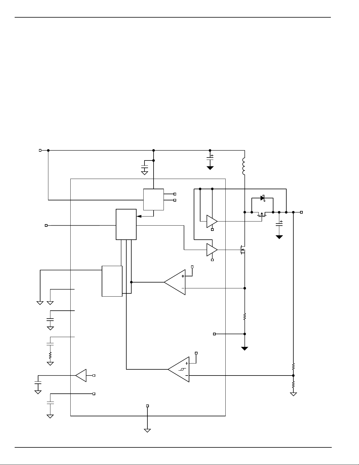
Figure 2. MIC2185 Skip Mode Block Diagram
MIC2185 8 December 2002
Page 9
MIC2185 Micrel
I
50mV
R
INDUCTOR_pk
SENSE
=
zero output current. This reduces parasitic ringing that
occurs during the discontinuous mode of operation found in
lightly loaded, non-synchronous boost converters. Pulling
the SKIP pin (pin 2) low will force the controller to operate in
PWM mode for all load conditions. Pulling the SKIP pin high
will force the controller to operate in SKIP mode.
Skip Mode Operation
This control method is used to improve efficiency at low
output loads. A block diagram of the MIC2185 skip mode is
shown in Figure 2. The power drawn by the MIC2185 control
IC is (I
VINA
· V
VINA
) + (I
VINP
· V
). The power dissipated by
VINP
the IC can be a significant portion of the total output power
during periods of low output current, which lowers the efficiency of the power supply. In skip mode the MIC2185 lowers
the IC supply current by disabling the high side drive and
running at lower than the PWM switching frequency. It also
turns off portions of the control and drive circuitry when the IC
is not switching. The disadvantage of this method is greater
output ripple and variable switching frequency. The Soft Start
and Sync pins have no effect when operating in skip mode.
In skip mode, switching starts when the feedback voltage
drops below the lower threshold level of the hysteresis
comparator. The OutN pin goes high, turning on the N-channel
MOSFET, Q1. Current ramps up in the inductor until either
the SKIP mode current limit comparator or the hysteretic
voltage comparator turns off Q1’s gate drive. If the feedback
voltage exceeds the upper hysteretic threshold, Q1’s gate
drive is terminated. Or, if the voltage at the CSH pin exceeds
the skip mode current limit threshold, it terminates the gate
drive for that switching cycle. The gate drive remains off for
a constant period at the end of each switching cycle. This off
time period is typically 1us when the F/2 pin is low and 2us
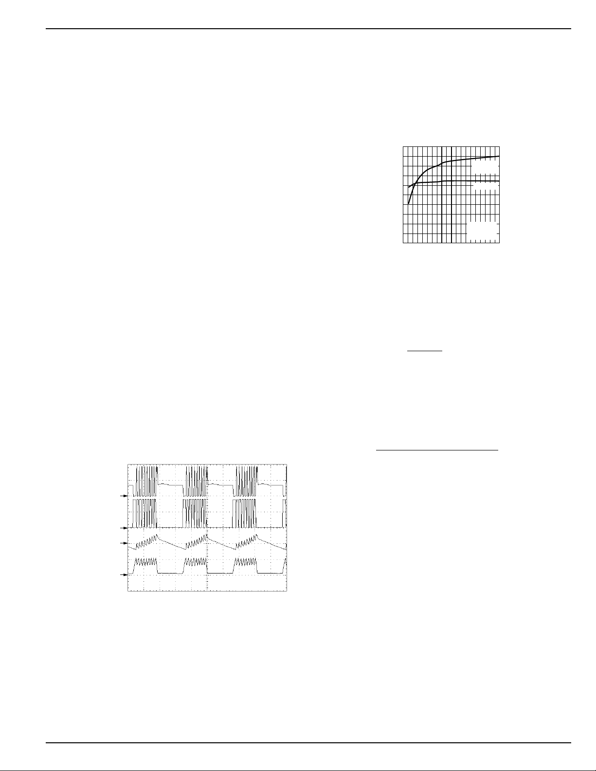
when the F/2 pin is high. Figure 3 shows some typical
switching waveforms in SKIP mode.
SKIP Mode Waveform
decrease until the feedback voltage drops below the lower
threshold voltage limit. The switching converter then turns the
gate drive back on. While the gate drive is disabled, the
MIC2185 draws less IC supply current then while it is switching, thereby improving efficiency at low output loads.
Figure 4 shows the improvement in efficiency that SKIP mode
makes when at lower output currents.
MIC2185 PWM vs.
Skip Mode Efficiency
100
0.08
0.1
PWM
400kHz
SKIP
VIN=3.3V
V
OUT
0.12
0.14
=5V
0.16
0.18
0.20
80
60
40
EFFICIENCY (%)
20
0
0
0.02
0.04
OUTPUT CURRENT (A)
0.06
Figure 4.
The maximum peak inductor current depends on the skip
current limit threshold and the value of the current sense
resistor, R
. For a typical 50mV current limit threshold
SENSE
in skip mode, the peak inductor current is:
The maximum output current in skip mode depends on the
input conditions, output conditions and circuit component
values. Assuming a discontinuous mode where the inductor
current starts from zero at each cycle, the maximum output
current is calculated below:
3
−
×××
2
η
()
()
O
IN
I
O(max)
=
2.5 10 L fs
2R V V
××−×
SENSE
Switch Node Voltage
(Low Side FET Drain)
V
OUT
5V/div
Low Side FET
Gate Drive
5V/div
Ripple Voltage
200mV/div
Inductor Current
5A/div
TIME (50µs/div)
VIN = 3.3V
= 9V
V
OUT
I
OUT
= 0.55A
where: I
VO is the output voltage
VIN is the input voltage
L is the value of the boost inductor
fS is the switching frequency
η is the efficiency of the boost converter
R
SENSE
2.5·10-3 is a constant based on the skip mode
current threshold (50mV)
is the maximum output current
O(max)
is the value of the current sense resistor
2
Figure 3. SKIP mode waveforms
The skip mode current threshold limits the peak inductor
current per cycle. Depending on the input, output and circuit
parameters, many switching cycles can occur before the
feedback voltage exceeds the upper hysteretic threshold.
Once the voltage on the feedback pin exceeds the upper
hysteretic threshold the gate drive is disabled. The output
load discharges the output capacitance causing Vout to
December 2002 9 MIC2185
Page 10
MIC2185 Micrel
PWM Operation
PWM Mode Waveform
Switch Node Voltage
(Low Side FET Drain)
1A offset; 0.5A/div
V
OUT
5V/div
High Side FET
Gate Drive
5V/div
Low Side FET
Gate Drive
5V/div
Inductor Current
Ripple Voltage
200mV/div
V
IN
= 3.3V
= 5V I
V
OUT
TIME (1µs/div)
OUT
= 0.75A
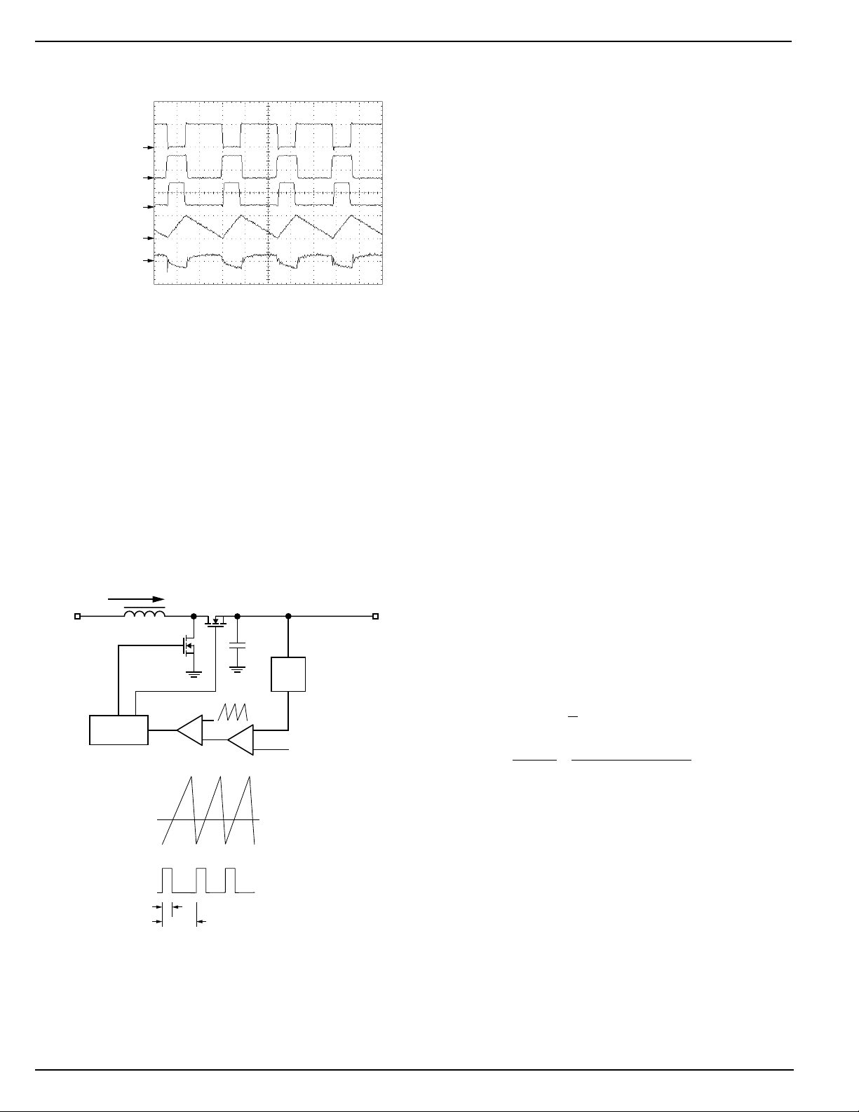
Figure 5 - PWM mode waveforms
Figure 5 shows typical waveforms for PWM mode of operation. The gate drive signal turns on the external low side
MOSFET, Q1, allowing the inductor current to ramp up.
When the low side MOSFET turns off and the high side
MOSFET, Q2, turns on, current flowing in the inductor forces
the MOSFET drain voltage to rise until the is clamped at
approximately the output voltage. The MIC2185 uses current
mode control to improve output regulation and simplify compensation of the control loop. Current mode control senses
both the output voltage (outer loop) and the inductor current
(inner loop). It uses the inductor current and output voltage to
determine the duty cycle (D) of the buck converter. Sampling
the inductor current effectively removes the inductor from the
control loop, which simplifies compensation. A simplified
current mode control diagram is shown in figure 6.
I_inductor
V
IN
Voltage
Divider
I_inductor
Gate Driver
V
I_inductor
I_inductor
V
COMP
Gate Drive at OUTN
T
ON
T
PER
REF
Figure 6. PWM Control Loop
A block diagram of the MIC2185 PWM current mode control
loop is shown in Figure 1. The inductor current is sensed by
measuring the voltage across a resistor, Rsense. The current
sense amplifier buffers and amplifies this signal. A ramp is
added to this signal to provide slope compensation, which is
required in current mode control to prevent unstable operation at duty cycles greater than 50%.
A transconductance amplifier is used as an error amplifier,
which compares an attenuated output voltage with a reference voltage. The output of the error amplifier is compared to
the current sense waveform in the PWM block. When the
current signal rises above the error voltage, the comparator
turns off the low side drive. The error signal is brought out to
the COMP pin (pin 4) allowing the use of external components to stabilize the voltage loop.
Current Sensing and Overcurrent Protection
The inductor current is sensed during the switch on time by
a current sense resistor located between the source of the
MOSFET, Q1 and ground (R
in Figure 1). Exceeding
SENSE
the current limit threshold will immediately terminate the gate
drive of the N-channel MOSFET. This forces the Q1 to
operate at a reduced duty cycle, which reduces the output
voltage. In a boost converter, the overcurrent limit will not
protect the power supply or load during a severe
overcurrent condition or short circuit condition. If the
output is short-circuited to ground, current will flow from the
input, through the inductor and output diode,D1, to ground.
Only the impedance of the source and components limits the
current.
The minimum input voltage, maximum output power and the
minimum value of the current limit threshold determine the
value of the current sense resistor. The two switch, synchronous operation of the MIC2185 forces the converter to always
operate in the continuous mode because current can flow
both ways through the high side P-channel MOSFET. The
equations below will help to determine the current sense
resistor value.
Maximum Peak Current
The peak inductor current is equal to the average inductor
current plus one half of the peak to peak inductor current.
The peak inductor current is:
II
=+×
IND(pk) IND(ave) IND(pp)
VI
=
V
OO
IN
I
IND(pk)
1
2
VVV
×
×
L
+
η
I
×−×
()
O
×××
2 V fs L
O
η
()
IN
where:
IO is the maximum output current
VO is the output voltage
VIN is the minimum input voltage
L is the value of the boost inductor
fS is the switching frequency
η is the efficiency of the boost converter
VL is the voltage across the inductor
VL December be approximated as V
for higher input
IN
voltage. However, the voltage drop across the inductor
winding resistance and low side MOSFET on-resistance
must be accounted for at the lower input voltages that the
MIC2185 can operate at.
MIC2185 10 December 2002
Page 11
MIC2185 Micrel
VV
DIODE_RRM OUT
=
VI
×
VV
=−
LIN
OO
V
×
IN
RR
×+
()
WINDING DS(ON)
η
where:
R
WINDING
R
DS(ON)
is the winding resistance of the inductor
is the on resistance of the low side switching
MOSFET
The maximum value of current sense resistor is:
V
R
SENSE
=
SENSE
I
IND(pk)
where:
V
is the minimum current sense threshold of
SENSE
the CSH pin
The current sense pin, CSH, is noise sensitive due to the low
signal level. The current sense voltage measurement is
referenced to the signal ground pin of the MIC2185. The
current sense resistor ground should be located close to the
IC ground. Make sure there are no high currents flowing in
this trace. The PCB trace between the high side of the current
sense resistor and the CHS pin should also be short and
routed close to the ground connection. The input to the
internal current sense amplifier has a 30nS dead time at the
beginning of each switching cycle. This dead time prevents
leading edge current spikes from prematurely terminating the
switching cycle. A small RC filter between the current sense
pin and current sense resistor December help to attenuate
larger switching spikes or high frequency switching noise.
Adding the filter slows down the current sense signal, which
has the effect of slightly raising the overcurrent limit threshold.
MOSFET Gate Drive
The MIC2185 synchronous boost converter drives both a
high side and low side MOSFET. The low side drive, OUTN,
drives an n-channel MOSFET. The high-side drive, OUTP, is
designed to switch a p-channel MOSFET (the p-channel
MOSFET doesn't require a bootstrap circuit which would be
needed to drive an n-channel MOSFET). The V
P pin must
IN
be connected to the output, which provides power to drive the
high and low side MOSFETs. In skip mode, the high side
MOSFET is disabled by forcing the OUTP pin to be high
(equal to V
OUT
).
MOSFET Selection
In a boost converter, the VDS of the MOSFET, Q1, is approximately equal to the output voltage. The maximum Vds rating
of the MOSFET must be high enough to allow for ringing and
spikes. The MIC2185 input voltage range is 2.9V to 14V.
MOSFETs with 20V and 30V V
ratings are ideal for use with
DS
this part.
The n-channel gate drive voltage is supplied by the OUTN
output. At startup in a boost converter, the output voltage
equals the input voltage. The VGS threshold voltage of the
n-channel MOSFET must be low enough to operate at the
minimum input voltage to guarantee the boost converter will
start up. The p-channel MOSFET must have a minimum
threshold voltage equal to or lower than the output voltage.
Five volt threshold (logic level) MOSFETs are recommended
for the p-channel MOSFET. Ringing in the gate drive signal
December cause MOSFETs with lower gate thresholds to
erroneously turn on.
There is a limit to the maximum amount of gate charge the
MIC2185 will drive. Higher gate charge will slow down the
turn-on and turn-off times of the MOSFETs. The MOSFET’s
must be able to completely turn on and off within the driver
non-overlap time or shoot-through will occur.
MOSFET gate charge is also limited by power dissipation in
the MIC2186. The power dissipated by the gate drive circuitry
is calculated below:
P
GATE_DRIVE
where: Q
GATE
=Q
GATE
· VINP · f
S
is the total gate charge of both of the external
n- and p-channel MOSFETs.
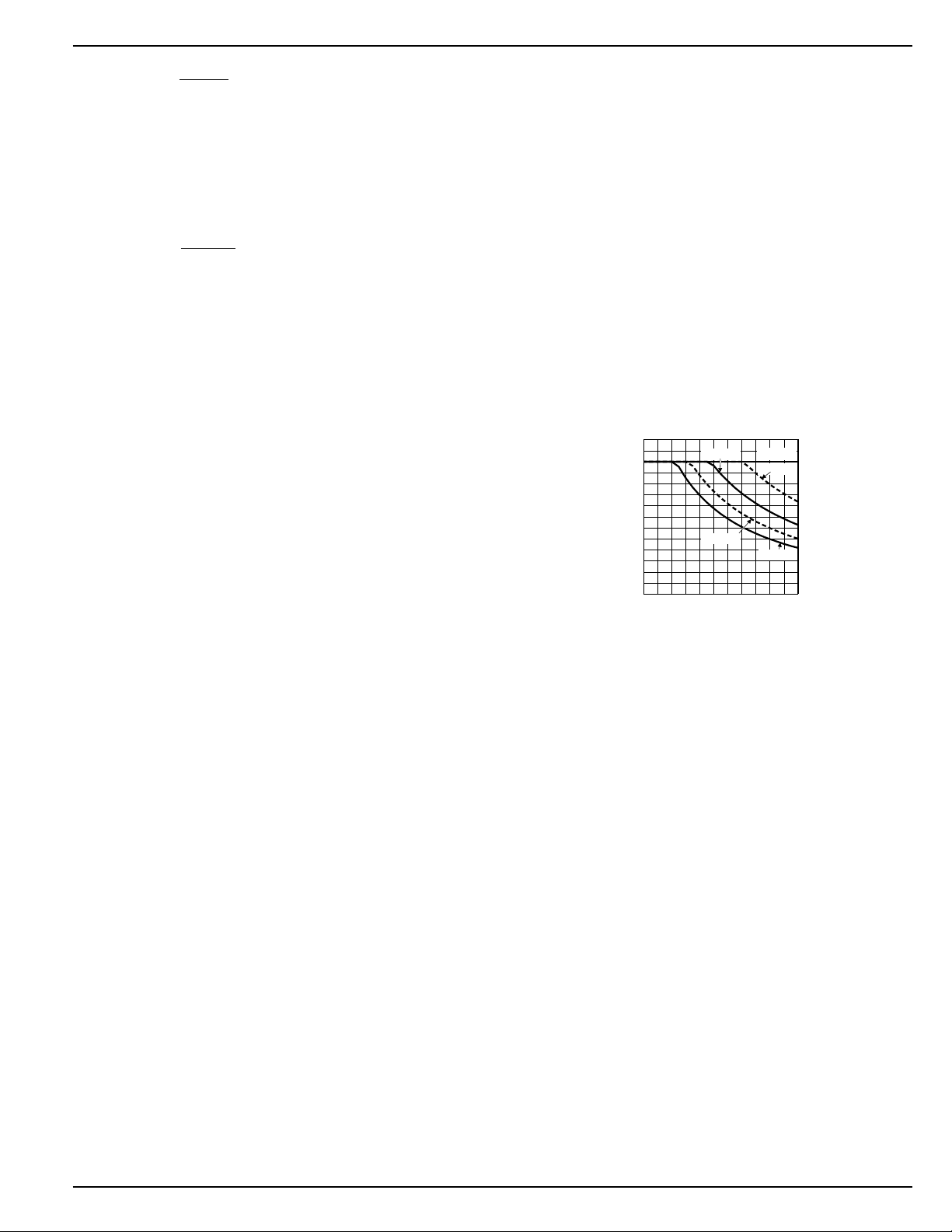
The graph in Figure 7 shows the total gate charge which can
be driven by the MIC2185 over the input voltage range, for
different values of switching frequency.
Frequency vs.
Maximum Gate Charge
140
120
100
80
60
40
20
TOTAL GATE CHARGE (nC)
0
35791113
400kHz
500kHz
INPUT VOLTAGE (V)
200kHz
300kHz
600kHz
Figure 7 - MIC2185 Frequency vs. Max. Gate Charge
External Schottky Diode
An external boost diode in parallel with the high side MOSFET
is used to keep the inductor current flow continuous during
the non-overlap time when both MOSFETs are turned off.
Although the average current through this diode is small, the
diode must be able to handle currents equal to the peak
inductor current. This peak current is calculated in the
Current Limit section of this specification
The reverse voltage requirement of the diode is:
For the MIC2185, Schottky diodes with a 30V or 40V rating
are recommended. Schottky diodes with lower reverse
voltage ratings have higher reverse leakage current which
will cause ringing and excessive power dissipation in the
diode and low side MOSFET.
The external Schottky diode is not necessary for circuit
operation since the high side MOSFET contains a parasitic
body diode. However, the body diode has a relatively slow
reverse recovery time and a relatively high forward voltage
drop. The lower forward voltage drop of the Schottky diode
both prevents the parasitic diode from turning on and improves efficiency. The lack of a reverse recovery mechanism
in a Schottky diode causes less ringing than the MOSFET's
parasitic diode. Depending on the circuit components and
December 2002 11 MIC2185
Page 12
MIC2185 Micrel
operating conditions, an external Schottky diode will improve
the converter efficiency by 1/2% to 1%.
Reference, Enable and UVLO Circuits
The output drivers are enabled when the following conditions
are satisfied:
• The VDD voltage (pin 10) is greater than its
undervoltage threshold.
• The voltage on the Enable pin is greater than
the Enable /UVLO threshold.
The internal bias circuitry generates a 1.245V bandgap
reference for the voltage error amplifier and a 3V V
voltage
DD
for the internal supply bus. The reference voltage in the
MIC2185 is buffered and brought out to pin 8. The VREF pin
must be bypassed to GND (pin 4) with a 0.1µF capacitor. The
VDD pin must be decoupled to ground with a 1µF ceramic
capacitor.
The Enable pin (pin 7) has two threshold levels, allowing the
MIC2185 to shut down in a micro-current mode, or turn off
output switching in standby mode. Below 0.9V (typical), the
device is forced into a low-power shutdown. If the enable pin
is between 0.9V and 1.5V (typical) the output gate drive is
disabled but the internal circuitry is powered on and the soft
start pin voltage is forced low. There is typically 140mV of
hysteresis below the 1.5V threshold to insure the part does
not oscillate on and off due to ripple voltage on the input.
Raising the Enable voltage above the UVLO threshold of
1.5V enables the output drivers and allows the soft start
capacitor to charge. The Enable pin December be pulled up
to VINA.
Oscillator & Sync
The internal oscillator is self-contained and requires no
external components. The f/2 pin allows the user to select
from two switching frequencies. A low level sets the oscillator
frequency to 400kHz and a high level sets the oscillator
frequency to 200kHz. The maximum duty cycle for both
frequencies is typically 85%. The minimum pulse width
increases but does not double when the frequency is changed
from 400kHz to 200kHz. This means the minimum duty cycle
is slightly lower at 200kHz. This December be important as
the input voltage approaches the output voltage. At lower
duty cycles, the input voltage can be closer to the output
voltage without the output rising out of regulation.
A frequency foldback mode is enabled if the voltage on the
Feedback pin (pin 6) is less than 0.3V. In frequency foldback
the oscillator frequency is reduced by approximately a factor
of 4. For the 400kHz setting, the oscillator runs at 100khz in
frequency foldback. For a 200kHz setting the oscillator runs
at approximately 50kHz.
The SYNC input (pin 11) allows the MIC2185 to synchronize
with an external CMOS or TTL clock signal. The rising edge
of the sync signal generates a reset signal in the oscillator,
which turns off the high side gate drive output. The low sidedrive then turns on, restarting the switching cycle. The sync
signal is inhibited when the controller operates in skip mode
or frequency foldback. The sync signal frequency must be
greater than the maximum specified free running frequency
of the MIC2185. If the synchronizing frequency is lower,
double pulsing of the gate drive outputs will occur. When not
used, the sync pin must be connected to ground.
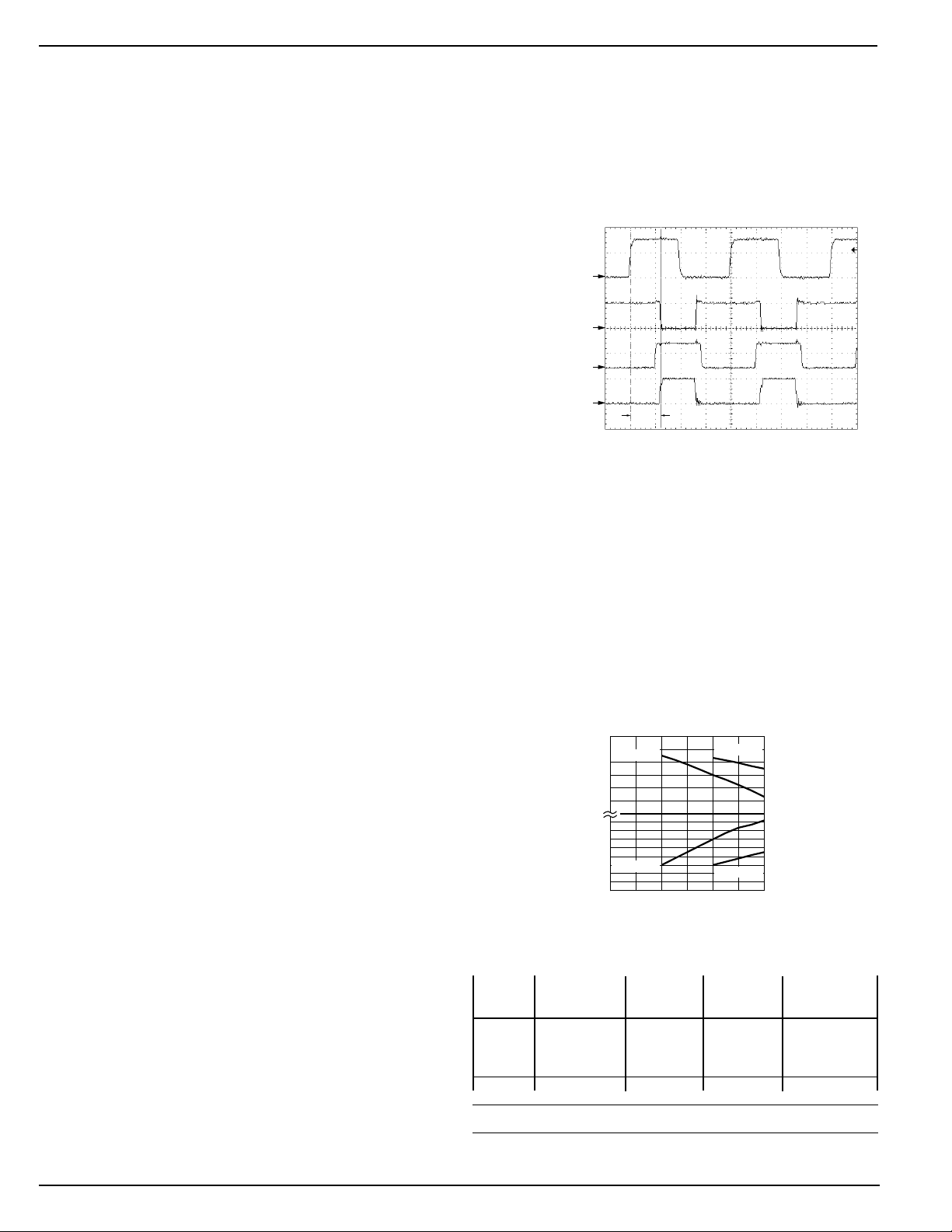
Figure 8 shows the timing between the external sync signal,
low side-drive and the high side drive when the f/2 pin is low.
The delay between the rising edge of the sync signal and the
turn on of the low side gate drive is typically 900ns when the
f/2 pin is high and 600ns when the f/2 pin is low.
Sync Waveform
Sync Input
2V/div
Switch Node Voltage
(Low Side FET Drain)
5V/div
High Side FET
Gate Drive
5V/div
Low Side FET
Gate Drive
5V/div
600ns
TIME (500ns/div)
Figure 8. Sync Waveforms
The maximum recommended output switching frequency is
600kHz. Synchronizing to higher frequencies December be
possible, however there are some concerns. As the switching frequency is increased, the switching period decreases.
The minimum on time in the MIC2185 becomes a greater part
of the total switching period. This December prevent proper
operation as Vin approaches Vout and December also minimize the effectiveness of the current limit circuitry. The
maximum duty cycle decreases as the sync frequency is
increased. Figure 9 shows the relationship between the
minimum and maximum duty cycle and frequency.
MIC2185 Sync Frequency
100
MAX. DUTY (%)
MIN. DUTY (%)
vs. Duty cycle
90
F/2 HIGH
80
70
60
50
40
18
16
14
12
10
8
6
F/2 HIGH
4
2
0
0 100 200 300 400 500 600
FREQUENCY (kHz)
F/2 LOW
F/2 LOW
Figure 9
Table 1 summarizes the differences in the MIC2185 for the
two different states of the f/2 pin.
F/2 pin Switching Typical Typical t
OFF
in
Level Frequency Max Duty Min. Duty SKIP Mode
(kHz) cycle (%) cycle (%)
0 400 85 6 1µs
1 200 85 6 2µs
MIC2185 12 December 2002
Page 13
MIC2185 Micrel
VV 1
R1
R2
O
REF
=×+
MIC2185 Table 1
Soft Start
Soft Start reduces the power supply input surge current at
start up by limiting the output voltage rise time. Input surge
current occurs when the boost converter charges up the
output capacitance. Slowing the output rise time lowers the
input surge current. Soft Start December also be used for
power supply sequencing. The soft start cannot control the
initial surge of current in a boost converter when V
is
IN
applied. This surge current is caused by the output capacitance charging up to the input voltage. The current flows from
the input through the inductor and output diode to the output
capacitors.
The soft start voltage is applied directly to the PWM comparator. A 5µA internal current source is used to charge up the soft
start capacitor. Either of 2 UVLO conditions will pull the soft
start capacitor low.
• When the VDD voltage drops below its UVLO
threshold
• When the Enable pin drops below the UVLO
threshold
The part switches at a low duty cycle when the soft start pin
voltage zero. As the soft start voltage rises from 0V to 0.7V,
the duty cycle increases from the minimum duty cycle to the
operating duty cycle. The oscillator runs at the foldback
frequency until the feedback voltage rises above 0.3V. In a
boost converter the output voltage is equal to the input
voltage before the MIC2185 starts switching. If the ratio of
Vout/Vin is low, the voltage on the feedback pin will already
be greater than 0.3V and the converter begin switching at the
selected operating frequency.
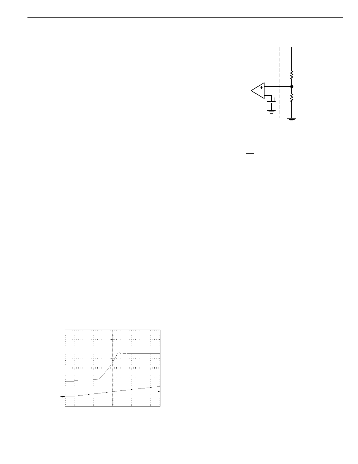
The risetime of the output is dependent on the soft start
capacitor, output capacitance, input and output voltage and
load current. The scope photo in Figure10 shows the output
voltage and the soft start pin voltage at startup. The output
voltage is initially at the input voltage less a diode drop. After
the converter is enabled the output slowly rises due to the
minimum duty cycle of the controller. As the soft start voltage
increases, the output voltage rises in a controlled fashion until
the output voltage reaches the regulated value.
Soft Start Waveform
VOUT
2V/div
VSS
1V/div
0V
TIME (2ms/div)
Figure 10 Soft Start
Voltage Setting Components
The MIC2185 requires two resistors to set the output voltage
as shown in Figure 11
MIC2185
Voltage
Amplifier
V
REF
1.245V
Pin
6
R1
R2
Figure 11
The output voltage is determined by the equation below.
where:
V
for the MIC2185 is nominally 1.245V.
REF
Lower values of resistance are preferred to prevent noise
from apprearing on the VFB pin. A typically recommended
value for R1 is 10kΩ.
Decoupling Capacitor Selection
A 1µF decoupling capacitor is used to stabilize the internal
regulator and minimize noise on the VDD pin. Placement of
this capacitor is critical to the proper operation of the MIC2185.
It must be next to the VDD and signal ground pins. The
capacitor should be a good quality ceramic. Incorrect placement of the VDD decoupling capacitor will cause jitter and/or
oscillations in the switching waveform as well as variations in
the overcurrent limit.
A minimum 0.1µF ceramic capacitor is required to decouple
the VIN pin. The capacitor should be placed near the IC and
connected directly between pin 10 (VDD) and pin 5 (SGND).
A 0.1µF capacitor is required to decouple VREF. It should be
located near the VREF pin.
Efficiency calculation and considerations
Efficiency is the ratio of output power to input power. The
difference is dissipated as heat in the boost converter. The
significant contributors at light output loads are:
• The VINA pin supply current.
• The VINP pin supply current which includes the
current required to switch the external
MOSFETs
• Core losses in the inductor
To maximize efficiency at light loads:
• Use a low gate charge MOSFET or use the
smallest MOSFET, which is still adequate for the
maximum output current.
• Allow the MIC2185 to run in skip mode at lower
currents. If running in PWM mode, set the
frequency to 200kHz.
• Use a ferrite material for the inductor core, which
December 2002 13 MIC2185
Page 14

MIC2185 Micrel
has less core loss than an MPP or iron power
core.
The significant contributors to power loss at higher output
loads are (in approximate order of magnitude):
• Resistive on-time losses in both MOSFETs
• Switching transition losses in the low side
MOSFET
• Inductor resistive losses
• Current sense resistor losses
• Output capacitor resistive losses (due to the
capacitor’s ESR)
To minimize power loss under heavy loads:
• Use logic level, low on-resistance MOSFETs.
Multiplying the gate charge by the on-resistance
gives a figure of merit, providing a good balance
between switching and resistive power dissipation.
• Slow transition times and oscillations on the
voltage and current waveforms dissipate more
power during the turn-on and turn-off of the low
side MOSFET. A clean layout will minimize
parasitic inductance and capacitance in the gate
drive and high current paths. This will allow the
fastest transition times and waveforms without
oscillations. Low gate charge MOSFETs will
switch faster than those with higher gate charge
specifications.
• For the same size inductor, a lower value will
have fewer turns and therefore, lower winding
resistance. However, using too small of a value
will increase the inductor current and therefore
require more output capacitors to filter the output
ripple.
• Lowering the current sense resistor value will
decrease the power dissipated in the resistor.
However, it will also increase the overcurrent
limit and December require larger MOSFETs
and inductor components to handle the higher
currents.
• Use low ESR output capacitors to minimize the
power dissipated in the capacitor’s ESR.
MIC2185 14 December 2002
Page 15
MIC2185 Micrel
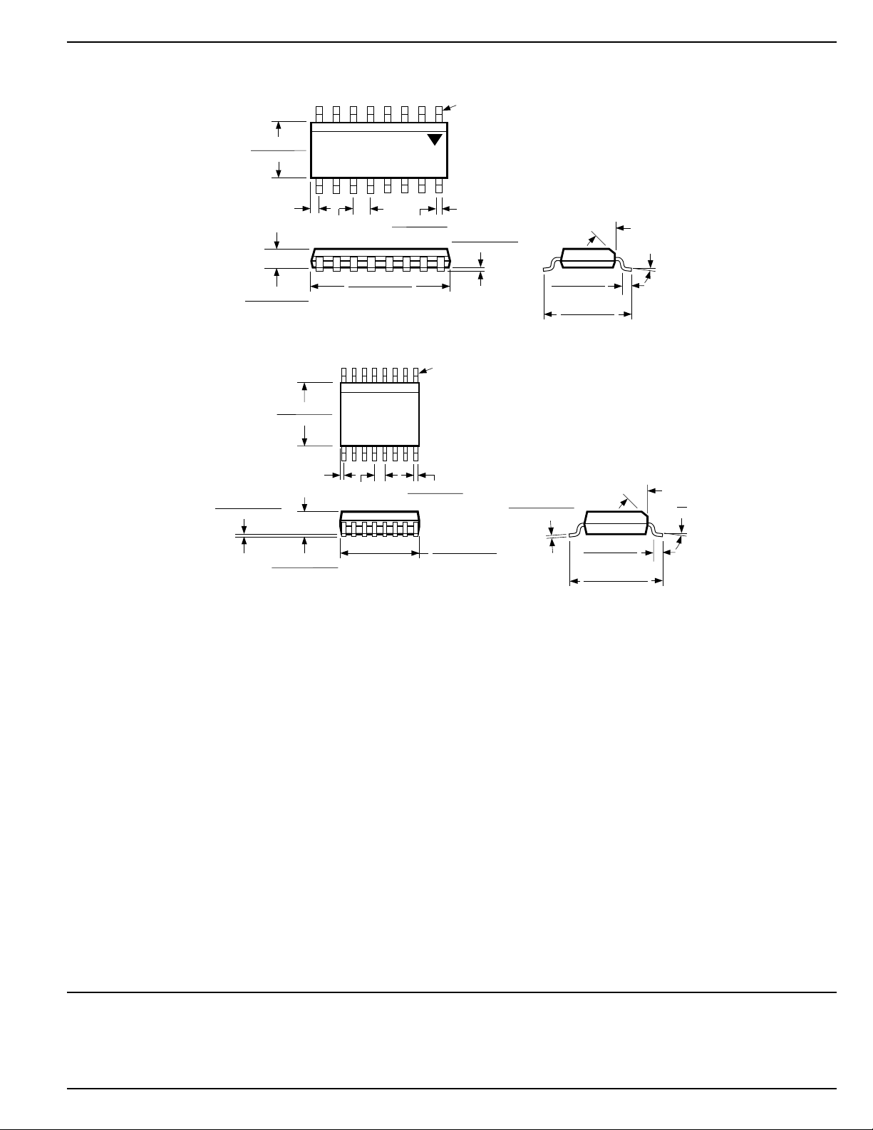
Package Information
PIN 1
0.157 (3.99)
0.150 (3.81)
0.020 (0.51)
REF
0.0648 (1.646)
0.0434 (1.102)
0.009 (0.2286)
0.0098 (0.249)
0.0040 (0.102)
SEATING
PLANE
0.050 (1.27)
0.157 (3.99)
0.150 (3.81)
REF
0.0688 (1.748)
0.0532 (1.351)
BSC
0.394 (10.00)
0.386 (9.80)
0.025 (0.635)
BSC
0.020 (0.51)
0.013 (0.33)
0.0098 (0.249)
0.0040 (0.102)
SEATING
PLANE
16-Pin SOIC (M)
PIN 1
0.012 (0.30)
0.008 (0.20)
0.196 (4.98)
0.189 (4.80)
DIMENSIONS:
INCHES (MM)
0.050 (1.27)
0.016 (0.40)
0.244 (6.20)
0.228 (5.79)
DIMENSIONS:
INCHES (MM)
0.0098 (0.249)
0.0075 (0.190)
45°
45°
0.050 (1.27)
0.016 (0.40)
0.2284 (5.801)
0.2240 (5.690)
0°–8°
8°
0°
16-Pin QSOP (QS)
MICREL INC. 1849 FORTUNE DRIVE SAN JOSE, CA 95131 USA
TEL + 1 (408) 944-0800 FAX + 1 (408) 944-0970 WEB http://www.micrel.com
This information is believed to be accurate and reliable, however no responsibility is assumed by Micrel for its use nor for any infringement of patents or
other rights of third parties resulting from its use. No license is granted by implication or otherwise under any patent or patent right of Micrel Inc.
© 2002 Micrel Incorporated
December 2002 15 MIC2185
 Loading...