

Page 1
MIC2184 Micrel
查询MIC2184供应商
MIC2184
Low Voltage Buck PWM Control IC
Final Information
General Description
Micrel’s MIC2184 is a high efficiency PWM buck control IC.
With its wide input voltage range of 2.9V to 14V, the MIC2184
can be used to efficiently step voltages down in 1- or 2-cell Li
Ion battery powered applications, as well as in fixed 3.3V, 5V,
or 12V systems.
Efficiencies over 90% are achievable over a wide range of
load conditions with the MIC2184’s PWM control scheme.
The operating frequency can be divided by two by raising the
FREQ/2 pin to VDD. This allows the user to optimize efficiency
versus board space. It also allows the MIC2184 to be externally synchronized to frequencies below its nominal 400KHz.
The MIC2184 features an oscillator output, FreqOut, which
can be used to implement a simple charge pump in low
voltage applications. The output of the charge pump can be
fed into the gate drive power circuitry via the V
allowing enhanced gate drive, hence higher efficiencies,
despite low input voltages.
MIC2184 features a 1µA shutdown mode, and a programmable undervoltage lockout, making it well suited for portable
applications.
The MIC2184 is available in 16 pin SOP and QSOP package
options with a junction temperture range range from –40°C
to +125°C.
P pin,
IN
Features
• Input voltage range: 2.9V to 14V
• >90% efficiency
• Oscillator frequency of 400kHz
• Frequency divide-by-two pin
• Frequency sync to 600kHz
• FrequOut oscillator output allows simple charge pump
implementation in low voltage systems
• 1.245V reference output
• Front edge blanking
•5Ω output driver
• Soft start
• PWM current mode control
•1µA shutdown current
• Cycle-by-cycle current limiting
• Frequency foldback short circuit protection
• Adjustable under-voltage lockout
• 16 pin narrow-body SOIC and QSOP package options
Applications
• 3.3V to 2.5V/1.8V/1.5V conversion
• DC power distribution systems
• Wireless Modems
• ADSL line cards
• 1-and 2-cell Li Ion battery operated equipment
• Satellite Phones
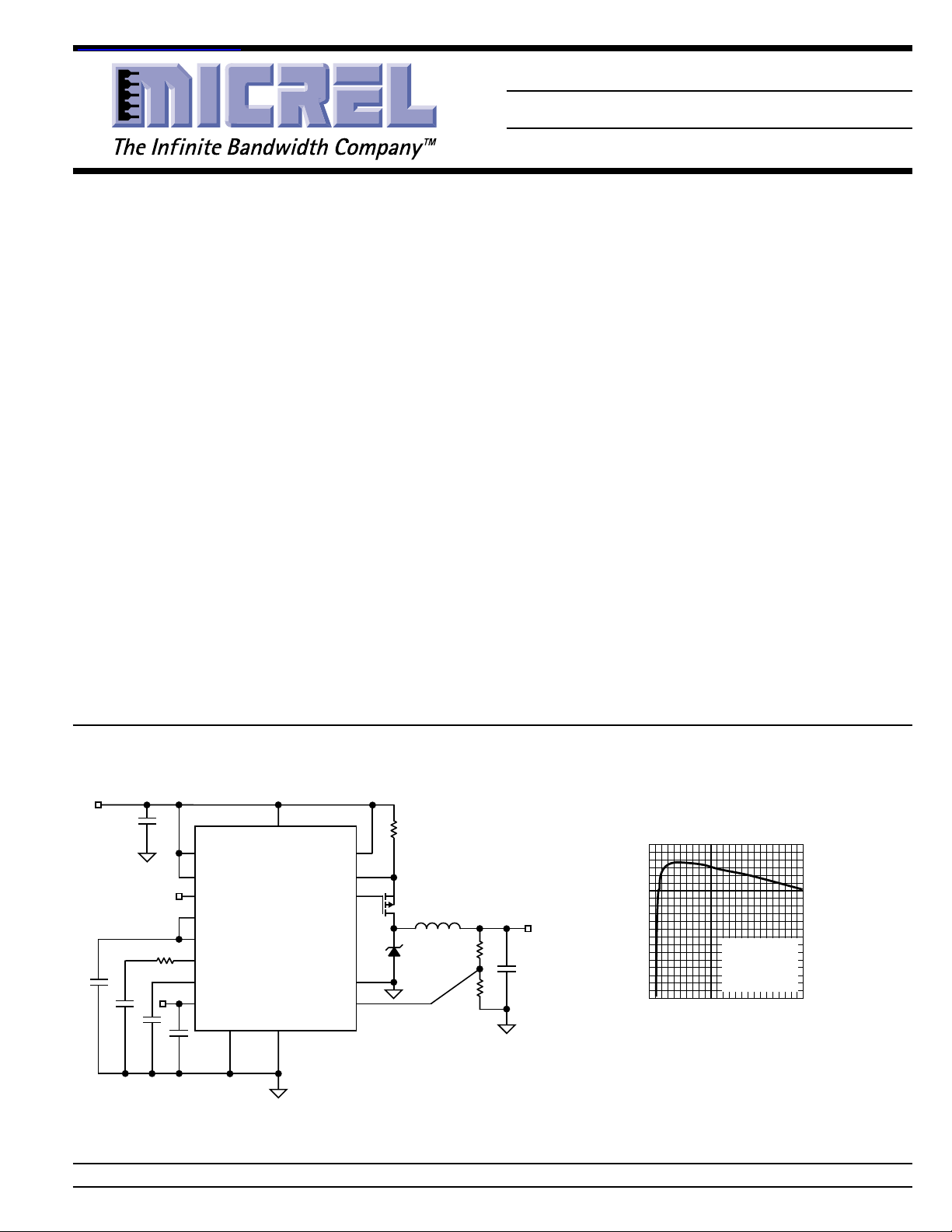
T ypical Application
= 3.3V
V
IN
120µF (x2)
6.3V
1
VINA
7
EN/UVLO
2
FreqOut
16
FREQ/2
10
VDD
4
COMP
3
SS
13
VREF
SYNC SGND
11 5
16
VINP
CSH
CSL
OUTP
MIC2184
PGND
FB
Adjustable Output Buck Converter
Micrel, Inc. • 1849 Fortune Drive • San Jose, CA 95131 • USA • tel + 1 (408) 944-0800 • fax + 1 (408) 944-0970 • http://www.micrel.com
December 10, 2001 1 MIC2184
9
8
14
12
6
15mΩ
Q3
Si9803DY(x2)
4.7µH
V
OUT
2.5V @5A
220µF(x2)
6.3V
MIC2184 EFFICIENCY
100
95
90
85
80
75
70
65
EFFICIENCY (%)
60
55
50
012345
OUTPUT CURRENT (A)
VIN = 3.3V
= 2.5V
V
OUT
= 200kHz
f
S
Page 2
MIC2184 Micrel
Ordering Information
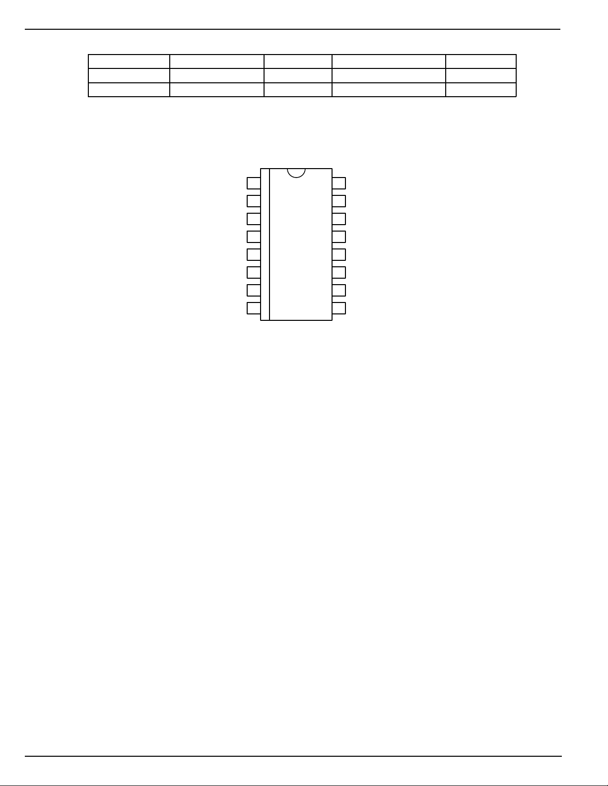
Part Number Output Voltage Frequency Junction Temp. Range Package
MIC2184BM Adjustable 400KHz –40°C to +125°C 16-lead SOP
MIC2184BQS Adjustable 400KHz –40°C to +125°C 16-lead QSOP
Pin Configuration
FreqOut
SS
COMP
SGND
FB
EN/UVLO
CSL
1VINA
2
3
4
5
6
7
8
16 Lead SOIC
(M)
16 VINP
FREQ/2
15
OUTP
14
VREF
13
PGND
12
SYNC
11
VDD
10
CSH
9
MIC2184 2 December 10, 2001
Page 3
MIC2184 Micrel
Pin Description
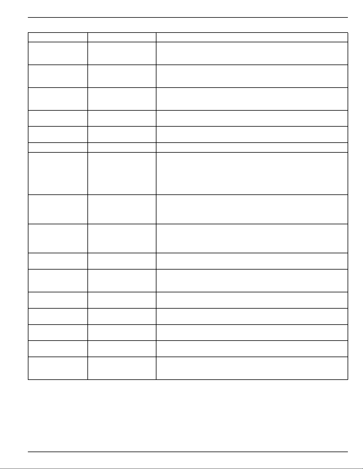
Pin Number Pin Name Pin Function
1 VINA Analog voltage input voltage to the circuit. This powers up the analog
sections of the die and does not need to be the same voltage as Pin 16
(VINP).
2 FreqOut This provides a digital signal output signal at half the switching frequency.
This signal swings from 0 to 3V, and can be used to drive an external
capacitive doubler to provide a higher voltage to the VINP input.
3 SS Soft start reduces the inrush current and delays and slows the output voltage
rise time. A 5µA current source will charge the capacitor up to V
capacitor will soft start the switching regulator in 1.5ms.
4 COMP Compensation (Output): Internal error amplifier output. Connect to a
capacitor or series RC network to compensate the regulator’s control loop.
5 SGND Small signal ground: must be routed separately from other grounds to the (-)
terminal of C
6 FB Feedback Input - the circuit regulates this pin to 1.245V.
7 EN/UVLO Enable/UnderVoltage Lockout (input): A low level on this pin will power down
the device, reducing the quiescent current to under 5uA. This pin has two
separate thresholds, below 1.5V the output switching is disabled, and below
0.9V the part is forced into a complete micropower shutdown. The 1.5V
threshold functions as an accurate undervoltage lockout (UVLO) with 140mV
hysteresis.
8 CSL The (-) input to the current limit comparator. A built in offset of 100mV
between CSH and CSL in conjunction with the current sense resistor sets
the current limit threshold level. This is also the (-) input to the current
amplifier.
9 CSH The (+) input to the current limit comparator. A built in offset of 100mV
between CSH and CSL in conjunction with the current sense resistor sets
the current limit threshold level. This is also the (+) input to the current
amplifier.
10 VDD 3V internal linear-regulator output. VDD is also the supply voltage bus for the
chip. Bypass to SGND with 1µF.
11 SYNC Frequency Synchronization (Input): Connect an external clock signal to
synchronize the oscillator. Leading edge of signal above 1.5V starts the
switching cycle. Connect to SGND if not used.
12 PGND MOSFET driver power ground, connects to source of synchronous MOSFET
and the (-) terminal of CIN.
13 VREF The 1.245V voltage reference is available on this pin. A 0.1µF capacitor
should be connected from this pin to ground.
14 OUTP High current drive for high side P channel MOSFET. Voltage swing is from
ground to VINP. On-resistance is typically 2.5Ω.
15 FREQ/2 When this is low, the oscillator frequency is 400KHz. When this pin is raised
to VDD, the oscillator frequency is 200KHz.
16 VINP Power Input voltage to the circuit. The output gate drivers are powered from
this supply. The current sense resistor R
possible to this pin.
OUT
.
should be connected as close as
CS
. A 1µF
DD
December 10, 2001 3 MIC2184
Page 4
MIC2184 Micrel
Absolute Maximum Ratings (Note 1)
Supply Voltage (V
Digital Supply Voltage (VDD) ...........................................7V
Comp Pin Voltage (V
Feedback Pin Voltage (VFB) .......................... –0.3V to +3V
Enable Pin Voltage (V
Current Sense Voltage (V
Sync Pin Voltage (V
Freq/2 Pin Voltage (V
A, VINP) .........................................15V
IN
)............................ –0.3V to +3V
COMP
EN/UVLO
SYNC
FREQ/2
) ..................... –0.3V to 15V
CSH–VCSL
) ............... –0.3V to 1V
) ................................ –0.3V to 7V
) ............................ -0.3V to 7V
Operating Ratings (Note 2)
Supply Voltage (V
Ambient Operating Temperature......... –40°C ≤ TA ≤ +85°C
Junction Temperature ....................... –40°C ≤ TJ ≤ +125°C
Output Voltage Range...................................... 1.3V to 12V
PackageThermal Resistance
θJA 16-lead SOP ...............................................100°C/W
θJA 16-lead QSOP.............................................163°C/W
A, VINP) ........................ +2.9V to +14V
IN
Power Dissipation (PD)
16 lead SOIC.................................400mW @ TA = 85°C
16 lead QSOP ...............................245mW @ TA = 80°C
Ambient Storage Temp ............................–65°C to +150°C
ESD Rating, ............................................................. Note 3
Electrical Characteristics
VINA = VINP = V
–40ºC < TJ < +125ºC.
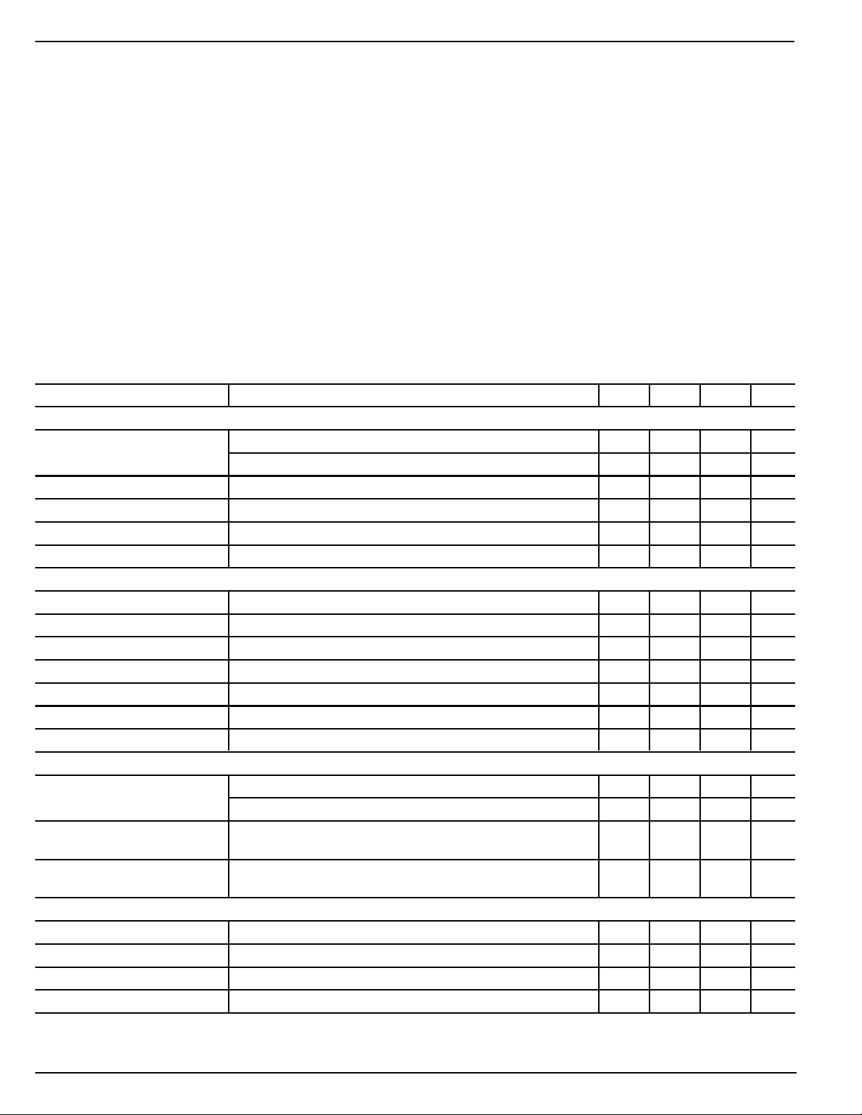
Parameter Condition Min Typ Max Units
Regulation
Feedback Voltage Reference (±1%) 1.233 1.245 1.257 V
Feedback Bias Current 50 nA
Output Voltage Line Regulation 5V ≤ VIN ≤ 12V 0.04 % / V
Output Voltage Load Regulation 0mV < (V
Output Voltage Total Regulation 5V ≤ VINA ≤ 12V, 0mV < (V
Input & VDD Supply
VINA Input Current 0.7 mA
VINP Input Current, Note 4 (Excluding external MOSFET gate current) 1.0 mA
Shutdown Quiescent Current V
Digital Supply Voltage (VDD)I
Digital Supply load regulation IL = 0 to 1mA 0.03 V
Undervoltage Lockout VDD upper threshold (turn on threshold) 2.75 V
UVLO Hysteresis 100 mV
Reference Output(VREF)
Reference Voltage (±1.5%) 1.226 1.245 1.264 V
Reference Voltage Line 5V < VINA < 12V 2 mV
Regulation
Reference Voltage Load 0 < I
Regulation
Enable/UVLO
Enable Input Threshold 0.6 0.9 1.2 V
UVLO Threshold (Turn-on threshold) 1.4 1.5 1.6 V
UVLO Hysteresis 140 mV
Enable Input Current V
CSH
= 5V, V
= 3.3V, V
OUT
EN/UVLO
(±2%) 1.22 1.27 V
EN/UVLO
= 0 2.82 3.0 3.18 V
L
(±2.5%) 1.213 1.276 V
REF
EN/UVLO
= 5V, V
– V
CSH
= 0V; (I
< 100µA1mV
= 5V 0.2 5 µA
) < 75mV 0.9 %
CSL
VINA
= 0V, TJ = 25ºC, unless otherwise specified. Bold values indicate
FREQ/2
– V
CSH
+ I
) 0.5 5 µA
VINP
) < 75mV (±3%) 1.208 1.282 V
CSL
MIC2184 4 December 10, 2001
Page 5
MIC2184 Micrel
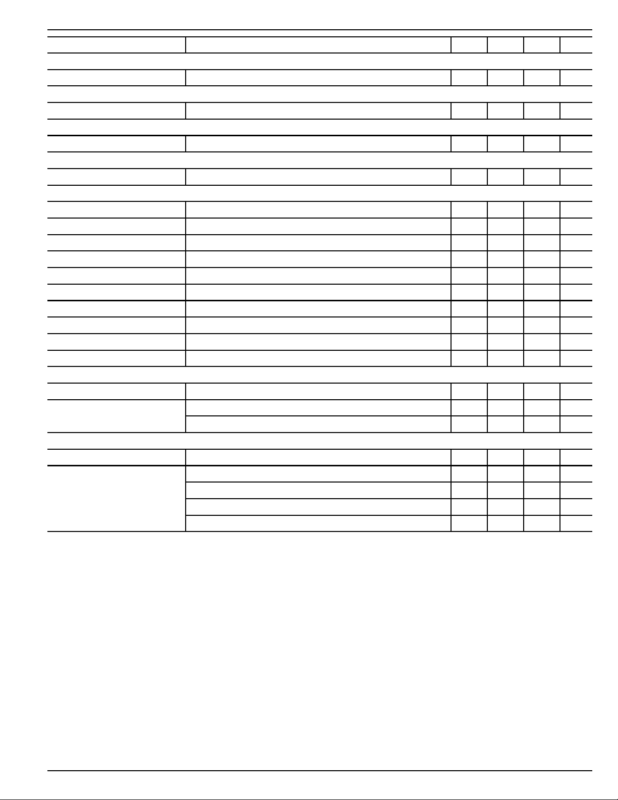
Parameter Condiion Min Typ Max Units
Soft Start
Soft Start Current 5 µA
Current Limit
Current Limit Threshold Voltage Voltage on CSH-CSL to trip current limit 100 mV
Error Amplifier
Error Amplifier Gain 20 V/V
Current Amplifier
Current Amplifier Gain 3.0 V/V
Oscillator Section
Oscillator Frequency (fO) 360 400 440 kHz
Maximum Duty Cycle VFB = 1.0V 100 %
Minimum On Time VFB = 1.5V 185 ns
Freq/2 Frequency (fO)V
Frequency Foldback Threshold Measured on FB 0.3 V
Frequency Foldback Frequency 90 kHz
SYNC Threshold Level 0.6 1.4 2.2 V
SYNC Input Current 0.1 5 µA
SYNC Minimum Pulse Width 200 ns
SYNC Capture Range Note 5
FreqOut Output
FreqOut Frequency Note 6 fO / 2 kHz
FreqOut Current Drive Sink 8mA
Source –6mA
Gate Drivers
Rise/Fall Time CL = 3300pF 50 ns
Output Driver Impedance Source; VINP = 12V 1.8 4 Ω
Sink; VINP = 12V 1.6 3.5 Ω
Source; VINP = 5V 2.6 Ω
Sink; VINP = 5V 2.4 Ω
= 5V 170 200 230 kHz
FREQ/2
fO +15 %
600 kHz
Note 1: Absolute maximum ratings indicate limits beyond which damage to the component may occur. Electrical specifications do not apply when
Note 2. The device is not guaranteed to function outside its operating rating.
Note 3. Devices are ESD sensitive. Handling precautions recommended.
Note 4: See application information for I(VINP) vs. VINP.
Note 5: See application information for limitations on maximum operating frequency.
Note 6: The frequency on FreqOut is half the frequency of the oscillator, or half the frequency of the external Sync signal.
operating the device outside of its operating ratings. The maximum allowable power dissipation is a function of the maximum junction
temperature, TJ(Max), the junction-to-ambient thermal resistance, θJA, and the ambient temperature, TA.
December 10, 2001 5 MIC2184
Page 6
MIC2184 Micrel
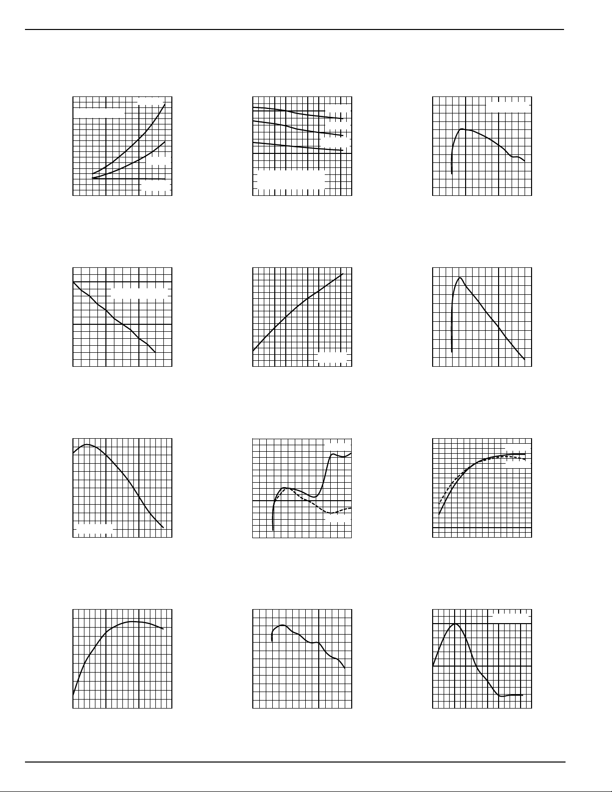
Typical Characteristics
Quiescent Current
vs. Input Voltage
4.5
4
IQ = I
+ I
VINA
3.5
3
2.5
2
1.5
1
0.5
QUIESCENT CURRENT (mA)
0
0 5 10 15
3.005
3.000
2.995
2.990
(V)
DD
2.985
V
2.980
2.975
2.970
0 0.2 0.4 0.6 0.8 1 1.2
VINP
INPUT VOLTAGE (V)
VDDvs. Load
VINA = VINP = 5V
VDD LOAD CURRENT (mA)
400kHz
200kHz
I
STANDBY
Quiescent Current
vs. Temperature
1.4
1.2
1.0
0.8
0.6
0.4
IQ = I
+ I
VINA
0.2
VINA = VINP = 3.3V
QUIESCENT CURRENT (mA)
0
-40 -20 0 20 40 60 80 100120140
VDDvs. Temperature
3.08
3.06
3.04
3.02
3.00
VDD (V)
2.98
2.96
2.94
2.92
-40 -20 0 20 40 60 80 100120140
VINP
TEMPERATURE (°C)
TEMPERATURE (°C)
400kHz
200kHz
I
STANDBY
VIN = 5V
VDDvs. Input Voltage
3.10
3.05
3.00
(V)
2.95
DD
V
2.90
2.85
2.80
0 5 10 15
INPUT VOLTAGE (V)
Error Amp Reference Voltage
vs. Input Voltage
1.2451
1.2449
1.2447
1.2445
1.2443
REFERENCE VOLTAGE (V)
1.2441
02468101214
INPUT VOLTAGE (V)
VINA = VINP
Error Amp Reference Voltage
1.246
1.245
1.244
1.243
1.242
1.241
REFERENCE VOLTAGE (V)
1.24
CURRENT (µA)
vs. Temperature
VIN = 3.3V
-40 -20 0 20 40 60 80 100120140
TEMPERATURE (°C)
Soft Start Current vs.
Temperature
4.9
4.8
4.7
4.6
4.5
4.4
-40 -20 0 20 40 60 80 100120140
TEMPERATURE (°C)
Frequency Variation
vs. Input Voltage
2
1.5
1
0.5
0
-0.5
-1
-1.5
FREQUENCY VARIATION (%)
-2
02468101214
INPUT VOLTAGE (V)
Overcurrent Threshold
102.0
100.0
98.0
96.0
94.0
THRESHOLD (mV)
92.0
90.0
vs. Input Voltage
02468101214
INPUT VOLTAGE (V)
200kHz
400kHz
Frequency Variation vs.
5
3
1
-1
-3
-5
-7
-9
-11
-13
SOFT START CURRENT (µA)
-15
-50 -30 -10 10 30 50 70 90 110
102
101
100
99
98
97
THRESHOLD (mV)
96
95
-40 -20 0 20 40 60 80 100120140
Temperature
200kHz
400kHz
TEMPERATURE (°C)
Overcurrent Threshold
vs. Temperature
VIN = 3.3V
TEMPERATURE (°C)
MIC2184 6 December 10, 2001
Page 7

MIC2184 Micrel
OUTP Drive Impedance vs.
Input Voltage
4
3.5
3
2.5
2
IMPEDANCE (Ω)
1.5
1
0 5 10 15
INPUT VOLTAGE (V)
SINK
SOURCE
December 10, 2001 7 MIC2184
Page 8
MIC2184 Micrel
Functional Diagram
V
IN
C
DECOUP
VINA
C
IN
1
OVERCURRENT
VREF
1.245V
COMPARATOR
0.1V
9
CSH
EN/UVLO
VDD
SYNC
FREQ/2
FreqOut
SS
COMP
VREF
7
10
fs/4
11
15
2
÷2
3
4
13
OSC
COMPARATOR
V
REF
VDD
CONTROL
RESET
SLOPE
COMPENSATION
PWM
BIAS
CURRENT
100k
fs/4
SENSE
AMP
∑
gm = 0.0002
gain = 20
FREQUENCY
FOLDBACK
ON
GAIN
3.7
V
ERROR
AMP
0.3V
REF
8
16
14
12
6
5
CSL
VINP
OUTP
PGND
FB
SGND
Q1
R
SENSE
D1
L1
C
OUT
V
OUT
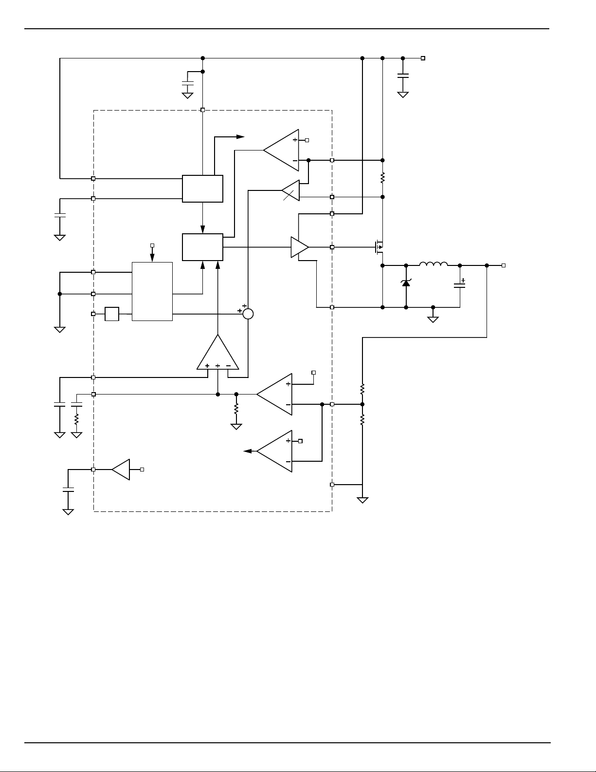
Figure 1. MIC2184 Block Diagram
Functional Characteristics
Controller Overview and Functional Description
The MIC2184 is a BiCMOS, switched mode, synchronous,
step down (buck) converter controller. It uses a P-Channel
MOSFET, which allows the controller to operate at 100% duty
cycle and eliminates the need for a high side drive bootstrap
circuit. Current mode control is used to achieve superior
transient line and load regulation. An internal corrective ramp
provides slope compensation for stable operation above a
50% duty cycle. The controller is optimized for high efficiency,
P-Channel MOSFET, Q1. Current flows from the input to the
output through the current sense resistor, MOSFET and
inductor. The current amplitude increases, controlled by the
inductor. The voltage developed across the current sense
resistor, R
, is amplified inside the MIC2184 and com-
SENSE
bined with an internal ramp for stability. This signal is compared to the output of the error amplifier. When the current
signal equals the error voltage signal, the P-channel MOSFET
is turned off. The inductor current flows through the diode, D1.
At the beginning of the next switching cycle, the P-channel
MOSFET is turned on which turns off the diode, D1.
high performance DC-DC converter applications.
Figure 1 is a block diagram of the MIC2184 configured as a
synchronous buck converter. At the beginning of the switching cycle, the OUTP pin pulls low and turns on the high-side
MIC2184 8 December 10, 2001
Page 9
MIC2184 Micrel
The MIC2184 controller is broken down into 7 functions.
• Control loop
• PWM operation
• Current mode control
• Current limit
• Reference, enable and UVLO
• FreqOut
• MOSFET gate drive
• Oscillator and Sync
• Soft-start
Control Loop
PWM Control Loop
The MIC2184 uses current mode control to regulate the
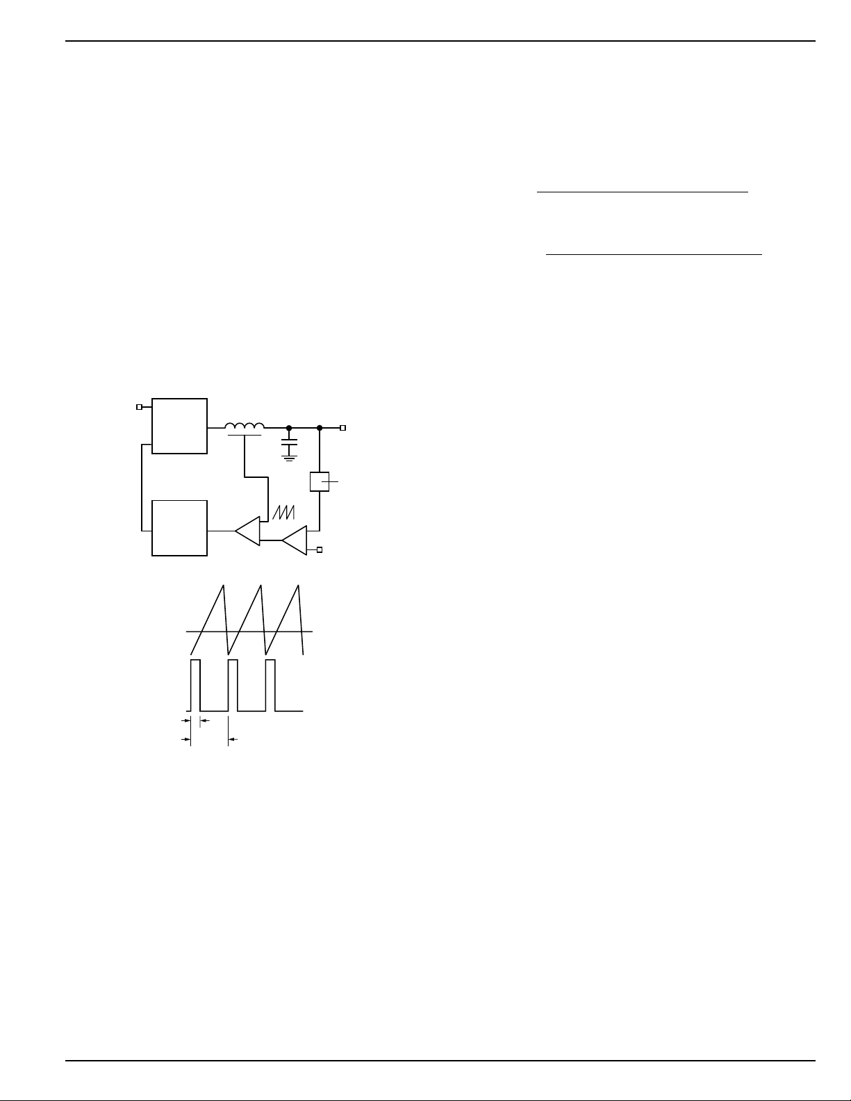
output voltage. This dual control loop method (illustrated in
Figure 2) senses the output voltage (outer loop) and the
inductor current (inner loop). It uses inductor current and
output voltage to determine the duty cycle of the buck
converter. Sampling the inductor current effectively removes
the inductor from the control loop, which simplifies compensation.
V
IN
Switching
Converter
Switch
Driver
I
V
ERROR
t
ON
t
PER
INDUCTOR
V
ERROR
D = tON/t
PER
I
INDUCTOR
V
REF
V
OUT
Voltage
Divider
Figure 2. Current Mode Control Example
As shown in Figure 1, the inductor current is sensed by
measuring the voltage across the resistor, R
SENSE
. A ramp is
added to the amplified current sense signal to provide slope
compensation, which is required to prevent unstable operation at duty cycles greater than 50%.
A transconductance amplifier is used for the error amplifier,
which compares an attenuated sample of the output voltage
with a reference voltage. The output of the error amplifier is
the compensation pin (Comp), which is compared to the
current sense waveform in the PWM block. When the current
signal becomes greater than the error signal, the comparator
turns off the high side drive. The COMP pin provides access
to the output of the error amplifier and allows the use of
external components to stabilize the voltage loop.
Current Limit
The output current is detected by the voltage drop across the
external current sense resistor (R
in Figure 1.). The
SENSE
current sense resistor must be sized using the minimum
current limit threshold. The external components must be
designed to withstand the maximum current limit. The current
sense resistor value is calculated by the equation below:
MIN CURRENT SENSE THRESHOLD
R
SENSE
___
=
I
_
OUT MAX
The maximum output current is:
MAX CURRENT SENSE THRESHOLD
I
OUT MAX
_
___
=
R
SENSE
The current sense pins CSH (pin 9) and CSL (pin 8) are noise
sensitive due to the low signal level and high input impedance. The PCB traces should be short and routed close to
each other. A small (1nF) capacitor across the pins will
attenuate high frequency switching noise.
When the peak inductor current exceeds the current limit
threshold, the overcurrent comparator turns off the high side
MOSFET for the remainder of the switching cycle, effectively
decreasing the duty cycle. The output voltage drops as
additional load current is pulled from the converter. When the
voltage at the feedback pin (FB) reaches approximately 0.3V,
the circuit enters frequency foldback mode and the oscillator
frequency will drop to 1/4 of the switching frequency. This
limits the maximum output power delivered to the load under
a short circuit condition.
Reference, Enable and UVLO Circuits
The output drivers are enabled when the following conditions
are satisfied:
• The VDD voltage (pin 10) is greater than its
undervoltage threshold.
• The voltage on the enable pin (pin 7) is greater
than the enable UVLO threshold.
The enable pin (pin 7) has two threshold levels, allowing the
MIC2184 to shut down in a low current mode, or turn off output
switching in standby mode. An enable pin voltage lower than
the shutdown threshold turns off all the internal circuitry and
places the MIC2184 in a micropower shutdown mode.
If the enable pin voltage is between the shutdown and
standby thresholds, the internal bias, VDD and reference
voltages are turned on. The soft start pin is forced low by an
internal discharge MOSFET. The output drivers are inhibited
from switching. The OUTP pin is in a high state and the OUTN
pin remains in a low state. Raising the enable voltage above
the standby threshold allows the soft start capacitor to charge
and enables the output drivers. The standby threshold is
specified in the electrical characteristics. A resistor divider
can be used with the enable pin to prevent the power supply
from turning on until a specified input voltage is reached. The
circuit in Figure 3 shows how to connect the resistors.
December 10, 2001 9 MIC2184
Page 10
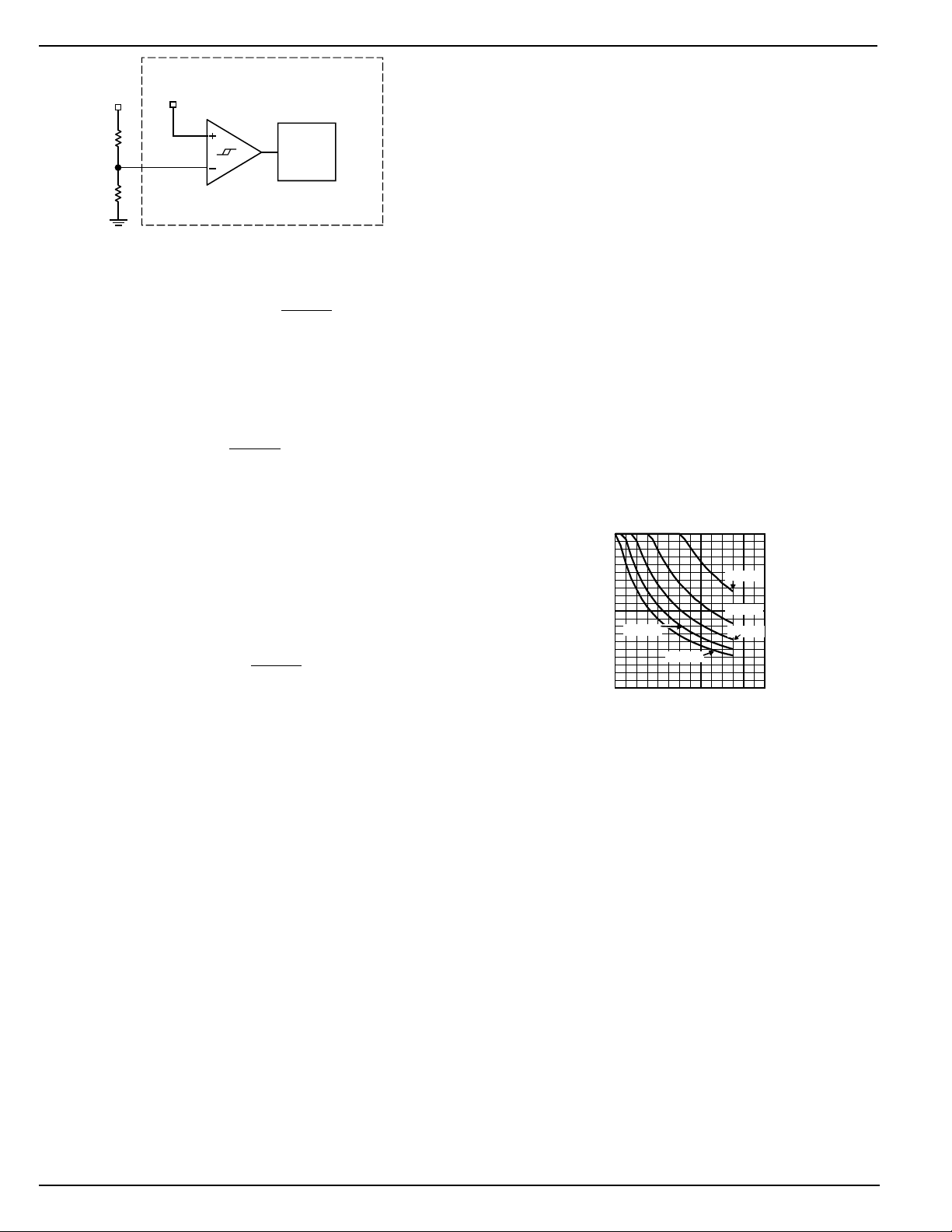
MIC2184 Micrel
MIC2184
1.5V
IN
Typical
EN/UVLO
(7)
140mV
Hysteresis
(typical)
Bias
Circuitry
V
R1
R2
Figure 3. UVLO Circuitry
The line voltage turn on trip point is:
VV
INPUT ENABLE
_
=×
THRESHOLD
R
RR
+212
where:
V
THRESHOLD
is the voltage level of the internal
comparator reference, typically 1.5V
The input voltage hysteresis is equal to:
RR
VV
INPUT HYST HYST_
=×
+12
R
2
where:
V
is the internal comparator hysteresis level,
HYST
typically 140mV.
V
INPUT_HYST
is the hysteresis at the input voltage
The MIC2184 will be disabled when the input voltage drops
back down to:
V
INPUT_OFF
V
INPUT_ENABLE
(V
THRESHOLD
=
– V
– V
INPUT_HYST
×
)
HYST
=
2
+RRR
12
Either of 2 UVLO conditions will pull the soft start capacitor
low.
• When the VDD voltage drops below its
undervoltage lockout level.
• When the enable pin drops below the its enable
threshold
The internal bias circuit generates an internal 1.245V bandgap reference voltage for the voltage error amplifier and a 3V
VDD voltage for the internal control circuitry. The V
REF
pin (pin
13) should be decoupled with a 0.1µf capacitor placed close
to the pin. The VDD pin must be decoupled with a 1µF ceramic
capacitor. The capacitor must be placed close to the VDD pin.
The other end of the capacitor must be connected directly to
the ground plane.
MOSFET Gate Drive
The MIC2184 is designed to drive a high side P-channel
MOSFET. The source pin of the P-channel MOSFET is
connected to the input of the power supply. It is turned on
when OUTP pulls the gate of the MOSFET low. The advantage of using a P-channel MOSFET is that it does not require
a bootstrap circuit to boost the gate voltage higher than the
input, as would be required for an N-channel MOSFET.
The VINP pin (pin 16) supplies the drive voltage to the gate
drive pin, OUTP. VINP pin is usually connected to the input
supply. The VINP pin and CSH pin must be connected to the
same potential.
MOSFET Selection
The P-channel MOSFET must have a VGS threshold voltage
equal to or lower than the input voltage when used in a buck
converter topology. There is a limit to the maximum gate
charge the MIC2184 will drive. Higher gate charge MOSFET
will slow down the turn-on and turn-off time of the MOSFET.
Slower transition times will cause higher power dissipation in
the MOSFET due to higher switching transition losses.
The MOSFET gate charge is also limited by power dissipation
in the MIC2184. The power dissipated by the gate drive
circuitry is calculated below:
P
GATE_DRIVE
=
QVPf
××
GATE
IN
S
where: Qgate is the total gate charge of both the N and Pchannel MOSFETs.
fS is the switching frequency
VINP is the gate drive voltage at the VINP pin
The graph in Figure 4 shows the total gate charge that can be
driven by the MIC2184 over the input voltage range, for
different values of switching frequency.
Frequency vs.
Max. Gate Charge
-9
200x10
-9
180x10
-9
160x10
-9
140x10
-9
120x10
-9
100x10
-9
80x10
500kHz
-9
60x10
-9
40x10
-9
TOTAL GATE CHARGE (C)
20x10
0
0x10
3 5 7 9 11 13 15 17
600kHz
INPUT VOLTAGE (V)
200kHz
300kHz
400kHz
Figure 4. MIC2184 Frequency vs Max. Gate Charge
Oscillator & Sync
The internal oscillator is free running and requires no external
components. The f/2 pin allows the user to select from two
switching frequencies. A low level set the oscillator frequency
to 400kHz and a high level set the oscillator frequency to
200kHz. The maximum duty cycle for both frequencies is
100%. This is another advantage of using a P-channel
MOSFET for the high-side drive; it can continuously turned
on.
A frequency foldback mode is enabled if the voltage on the
feedback pin (pin 6) is less than 0.3V. In frequency foldback,
the oscillator frequency is reduced by approximately a factor
of 4. Frequency foldback is used to limit the energy delivered
to the output during a short circuit fault condition.
The SYNC input (pin 11) lets the MIC2184 synchronize with
an external clock signal. The rising edge of the sync signal
generates a reset signal in the oscillator, which turns off the
low side gate drive output. The high side drive then turns on,
restarting the switching cycle. The sync signal is inhibited
when the controller operates in frequency foldback. The sync
signal frequency must be greater than the maximum speci-
MIC2184 10 December 10, 2001
Page 11
MIC2184 Micrel
fied free running frequency of the MIC2184. If the synchronizing frequency is lower, double pulsing of the gate drive
outputs will occur. When not used, the sync pin must be
connected to ground.
The maximum recommended output switching frequency is
600kHz. Synchronizing to higher frequencies may be possible, however, higher power dissipation in the internal gate
drive circuits will occur. The MOSFET gates require charge
to turn on the device. The average current required by the
MOSFET gate increases with switching frequency.
Soft Start
Soft start reduces the power supply input surge current at
start up by controlling the output voltage risetime. The input
surge appears while the output capacitance is charged up. A
slower output risetime will draw a lower input surge current.
Soft start may also be used for power supply sequencing.
The soft start voltage is applied directly to the PWM comparator. A 5µA internal current source is used to charge up the soft
start capacitor. The capacitor is discharged when either the
enable pin voltage drops below the standby threshold or the
VDD voltage drops below its UVLO level.
The part switches at a low duty cycle when the soft start pin
voltage is zero. As the soft start voltage rises from 0V to 0.7V,
the duty cycle increases from the minimum duty cycle to the
operating duty cycle. The oscillator runs at the foldback
frequency (1/4 of the switching frequency) until the feedback
voltage rises above 0.3V. The risetime of the output is
dependent of the soft start capacitor output capacitance,
input and output voltage and load current.
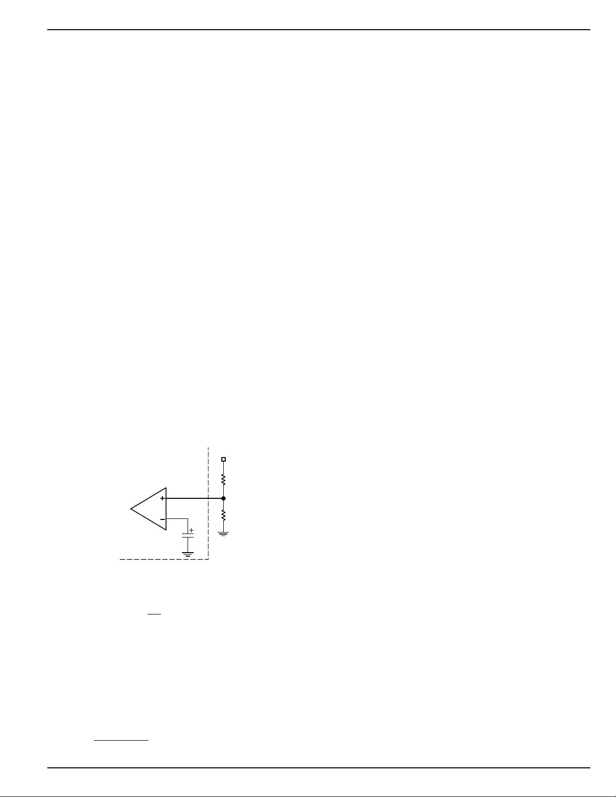
Voltage Setting Components
The MIC2184 requires two resistors to set the output voltage
as shown in Figure 5.
V
MIC2184
Voltage
Amplifier
V
1.245V
REF
OUT
R1
Pin 6
R2
Figure 5
The output voltage is determined by the equation below.
R
VV
OUT
Where: V
=×+1
REF
for the MIC2184 is typically 1.245V.
REF
1
R
2
Lower values of R1 are preferred to prevent noise from
appearing on the FB pin. A typically recommended value is
10kΩ. If R1 is too small in value it will decrease the efficiency
of the power supply, especially at low output loads.
Once R1 is selected, R2 can be calculated with the following
formula.
Efficiency Considerations
Efficiency is the ratio of output power to input power. The
difference is dissipated as heat in the buck converter. Under
light output load, the significant contributors are:
• The VINA supply current
• The VINP supply current, which includes the current
required to switch the external MOSFET
• Core losses in the output inductor
To maximize efficiency at light loads:
• Use a low gate charge MOSFET or use the smallest
MOSFET, which is still adequate for maximum output
current.
• Use a ferrite material for the inductor core, which has
less core loss than an MPP or iron power core.
Under heavy output loads the significant contributors to
power loss are (in approximate order of magnitude):
• Resistive on time losses in the MOSFET
• Switching transition losses in the MOSFET
• Inductor resistive losses
• Current sense resistor losses
• Input capacitor resistive losses (due to the capacitors
ESR)
To minimize power loss under heavy loads:
• Use low on resistance MOSFETs. Use low threshold
logic level MOSFETs when the input voltage is below
5V. Multiplying the gate charge by the on resistance
gives a figure of merit, providing a good balance
between low load and high load efficiency.
• Slow transition times and oscillations on the voltage
and current waveforms dissipate more power during
the turn on and turn off of the MOSFET. A clean
layout will minimize parasitic inductance and capaci
tance in the gate drive and high current paths. This
will allow the fastest transition times and waveforms
without oscillations. Low gate charge MOSFETs will
transition faster than those with higher gate charge
requirements.
• For the same size inductor, a lower value will have
fewer turns and therefore, lower winding resistance.
However, using too small of a value will require more
output capacitors to filter the output ripple, which will
force a smaller bandwidth, slower transient response
and possible instability under certain conditions.
• Lowering the current sense resistor value will de
crease the power dissipated in the resistor. However,
it will also increase the overcurrent limit and will
require larger MOSFETs and inductor components.
• Use low ESR input capacitors to minimize the power
dissipated in the capacitors ESR.
VR
×
R
REF
21=
VV
–
OUT
REF
December 10, 2001 11 MIC2184
Page 12
MIC2184 Micrel
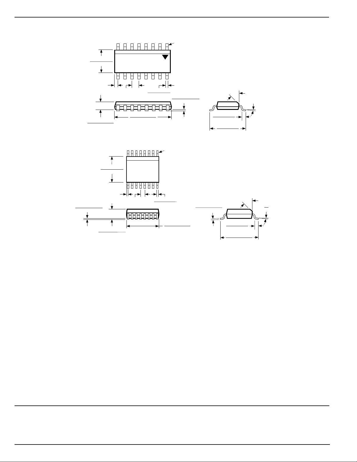
Package Information
PIN 1
0.157 (3.99)
0.150 (3.81)
0.020 (0.51)
REF
0.0648 (1.646)
0.0434 (1.102)
0.009 (0.2286)
0.0098 (0.249)
0.0040 (0.102)
SEATING
PLANE
0.050 (1.27)
0.157 (3.99)
0.150 (3.81)
REF
0.0688 (1.748)
0.0532 (1.351)
BSC
0.394 (10.00)
0.386 (9.80)
0.025 (0.635)
BSC
0.020 (0.51)
0.013 (0.33)
0.0098 (0.249)
0.0040 (0.102)
SEATING
PLANE
16-Pin SOP (M)
PIN 1
0.012 (0.30)
0.008 (0.20)
0.196 (4.98)
0.189 (4.80)
DIMENSIONS:
INCHES (MM)
0.050 (1.27)
0.016 (0.40)
0.244 (6.20)
0.228 (5.79)
DIMENSIONS:
INCHES (MM)
0.0098 (0.249)
0.0075 (0.190)
45°
45°
0.050 (1.27)
0.016 (0.40)
0.2284 (5.801)
0.2240 (5.690)
0°–8°
8°
0°
16-Pin QSOP (QS)
MICREL INC. 1849 FORTUNE DRIVE SAN JOSE, CA 95131 USA
TEL + 1 (408) 944-0800 FAX + 1 (408) 944-0970 WEB http://www.micrel.com
This information is believed to be accurate and reliable, however no responsibility is assumed by Micrel for its use nor for any infringement of patents or
other rights of third parties resulting from its use. No license is granted by implication or otherwise under any patent or patent right of Micrel Inc.
© 2001 Micrel Incorporated
MIC2184 12 December 10, 2001
 Loading...