

Page 1
MIC2171 Micrel
MIC2171
100kHz 2.5A Switching Regulator
Preliminary Information
General Description
The MIC2171 is a complete 100kHz SMPS current-mode
controller with an internal 65V 2.5A power switch.
Although primarily intended for voltage step-up applications,
the floating switch architecture of the MIC2171 makes it
practical for step-down, inverting, and Cuk configurations as
well as isolated topologies.
Operating from 3V to 40V, the MIC2171 draws only 7mA of
quiescent current, making it attractive for battery operated
supplies.
The MIC2171 is available in a 5-pin TO-220 or TO-263 for
–40°C to +85°C operation.
Features
• 2.5A, 65V internal switch rating
• 3V to 40V input voltage range
• Current-mode operation, 2.5A peak
• Internal cycle-by-cycle current limit
• Thermal shutdown
• Twice the frequency of the LM2577
• Low external parts count
• Operates in most switching topologies
• 7mA quiescent current (operating)
• Fits LT1171/LM2577 TO-220 and TO-263 sockets
Applications
• Laptop/palmtop computers
• Battery operated equipment
• Hand-held instruments
• Off-line converter up to 50W
(requires external power switch)
• Predriver for higher power capability
4
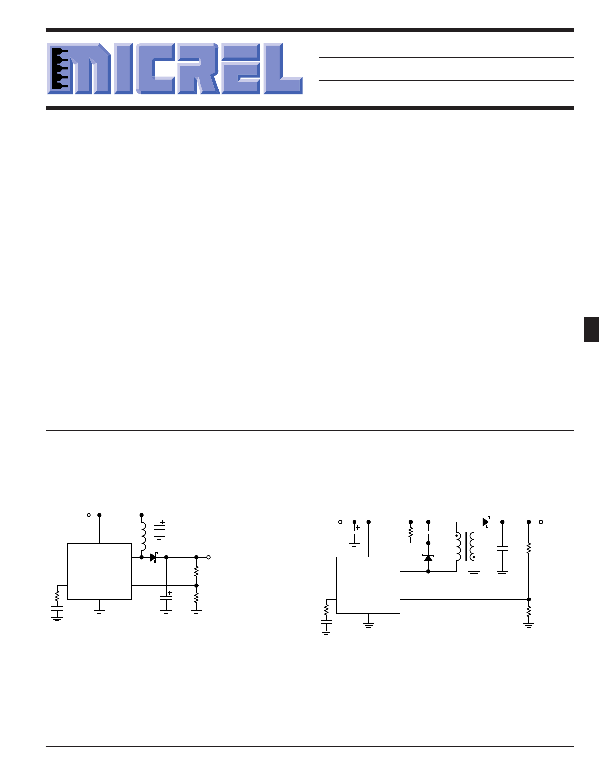
Typical Applications
+5V
(4.75V min.)
IN
MIC2171
COMP
3
1k
* Locate near MIC2171 when supply leads > 2
C3
1µF
GND
SW
FB
15µH
L1
MIC2171 5V to 12V Boost Converter
D1
1N5822
Figure 1.
C1*
47µF
C2
470µF
V
OUT
+12V, 0.25A
R1
10.7k
1%
R2
1.24k
1%
"
V
IN
4V to 6V
C1
47µF
IN
MIC2171
COMP
R3
1k
* Optional voltage clipper (may be req’d if T1 leakage inductance too high)
C2
1µF
GND
R4*
SW
FB
L
C3*
D1*
PRI
1:1.25
= 12µH
T1
D2
1N5818
470µF
Figure 2.
MIC2171 5V Flyback Converter
C4
R1
3.74k
1%
R2
1.24k
1%
V
OUT
5V, 0.5A
1997 4-3
Page 2
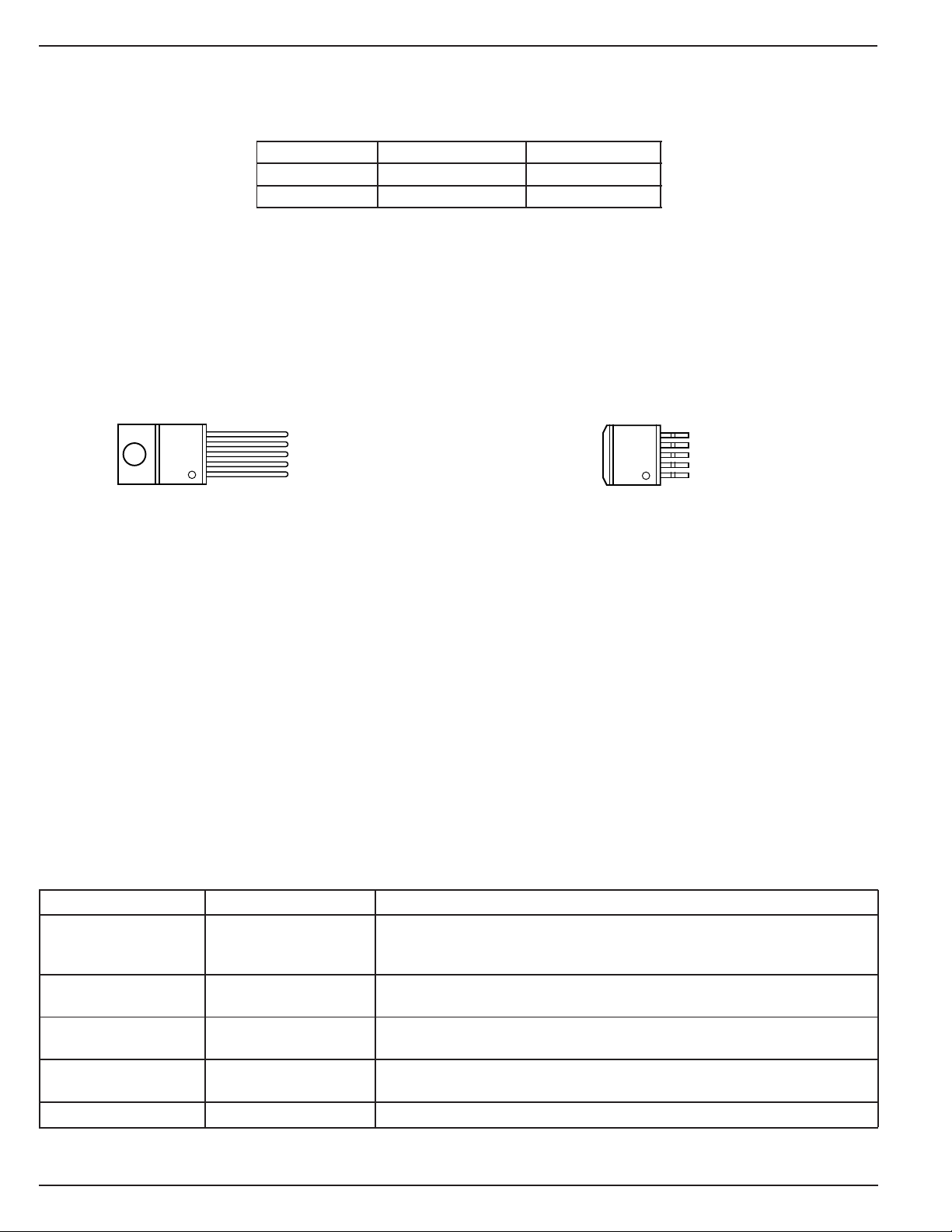
MIC2171 Micrel
5IN
4SW
3 GND
2FB
1 COMP
Ordering Information
Part Number Temperature Range Package
MIC2171BT –40°C to +85°C 5-lead TO-220
MIC2171BU –40°C to +85°C 5-lead TO-263
Pin Configuration
5IN
4SW
3 GND
2FB
1 COMP
Tab GND
Pin Description
Pin Number Pin Name Pin Function
1 COMP Frequency Compensation: Output of transconductance-type error amplifier.
2 FB Feedback: Inverting input of error amplifier. Connect to external resistive
3 GND Ground: Connect directly to the input filter capacitor for proper operation
4 SW Power Switch Collector: Collector of NPN switch. Connect to external
5 IN Supply Voltage: 3.0V to 40V
5-lead TO-263 (BU)5-lead TO-220 (BT)
Primary function is for loop stabilization. Can also be used for output voltage
soft-start and current limit tailoring.
divider to set power supply output voltage.
(see applications info).
inductor or input voltage depending on circuit topology.
4-4 1997
Page 3

MIC2171 Micrel
Absolute Maximum Ratings
Input Voltage (VIN) ........................................................40V
Switch Voltage (VSW)....................................................65V
Feedback Voltage (transient, 1ms) (VFB)................... ±15V
Operating Temperature Range ......................–40 to +85°C
Junction Temperature ................................–55°C to 150°C
Thermal Resistance
θJA 5-lead TO-220, Note 1.................................45°C/W
θJA 5-lead TO-263, Note 2.................................45°C/W
Storage Temperature ...............................–65°C to +150°C
Soldering (10 sec.) ..................................................+300°C
Electrical Characteristics
VIN = 5V; TA = 25°C, bold values indicate –40°C ≤ TA ≤ +85°C; unless noted.
Parameter Conditions Min Typ Max Units
Reference Section
Feedback Voltage (V
Feedback Voltage 3V ≤ V
Line Regulation V
Feedback Bias Current (I
Error Amplifier Section
Transconductance (g
Voltage Gain (AV) 0.9V ≤ V
Output Current V
)V
FB
)V
FB
) ∆I
m
COMP
COMP
= 1.24V 310 750 nA
FB
COMP
COMP
= 1.24V 1.220 1.240 1.264 V
1.214 1.274 V
≤ 40V .06 %/V
IN
= 1.24V
1100 nA
= ±25µA 3.0 3.9 6.0 µA/mV
2.4 7.0 µA/mV
≤ 1.4V 400 800 2000 V/V
COMP
= 1.5V 125 175 350 µA
100 400 µA
4
Output Swing High Clamp, V
= 1V 1.8 2.1 2.3 V
FB
Low Clamp, VFB = 1.5V 0.25 0.35 0.52 V
Compensation Pin Duty Cycle = 0 0.8 0.9 1.08 V
Threshold 0.6 1.25 V
Output Switch Section
ON Resistance I
= 2A, VFB = 0.8V 0.37 0.50 Ω
SW
0.55 Ω
Current Limit Duty Cycle = 50%, T
Duty Cycle = 50%, T
≥ 25°C 2.5 3.6 5 A
J
< 25°C 2.5 4.0 5.5 A
J
Duty Cycle = 80%, Note 3 2.0 3.0 5 A
Breakdown Voltage (BV) 3V ≤ VIN ≤ 40V 65 75 V
ISW = 5mA
Oscillator Section
Frequency (f
) 88 100 112 kHz
O
85 115 kHz
Duty Cycle [δ(max)] 80 90 95 %
Input Supply Voltage Section
Minimum Operating Voltage 2.7 3.0 V
Quiescent Current (IQ) 3V ≤ VIN ≤ 40V, V
Supply Current Increase (∆IIN) ∆ISW = 2A, V
General Note Devices are ESD sensitive. Handling precautions required.
Note 1 Mounted vertically, no external heat sink, 1/4 inch leads soldered to PC board containing approximently 4 inch squared copper area
surrounding leads.
Note 2 All ground leads soldered to approximently 2 inches squared of horizontal PC board copper area.
Note 3 For duty cycles (δ) between 50% and 95%, minimum guaranteed switch current is ICL = 1.66 (2-δ) Amp (Pk).
COMP
= 0.6V, ISW = 0 7 9 mA
COMP
= 1.5V, during swich on-time 9 20 mA
1997 4-5
Page 4

MIC2171 Micrel
Typical Performance Characteristics
Minimum
Operating Voltage
2.9
2.8
2.7
2.6
Switch Current = 2A
2.5
2.4
Minimum Operating Voltage (V)
2.3
-100 -50 0 50 100 150
15
14
13
12
11
10
Supply Current (mA)
Temperature (°C)
Supply Current
ISW = 0
D.C. = 90%
D.C. = 50%
9
8
D.C. = 0%
7
6
5
0 10203040
VIN Operating Voltage (V)
Feedback Bias Current
800
700
600
500
400
300
200
100
Feedback Bias Current (nA)
0
-100 -50 0 50 100 150
Temperature (°C)
50
40
30
20
10
Average Supply Current (mA)
Supply Current
δ = 90%
δ = 50%
0
01234
Switch Current (A)
Feedback Voltage
Line Regulation
5
4
3
2
1
0
-1
-2
-3
-4
Feedback Voltage Change (mV)
-5
0 10203040
10
V
9
COMP
8
7
6
5
4
3
Supply Current (mA)
2
1
0
-100 -50 0 50 100 150
TJ = 125°C
TJ = 25°C
TJ = -40°C
VIN Operating (V)
Supply Current
= 0.6V
Temperature (°C)
Switch On-Voltage
1.6
1.4
1.2
1.0
0.8
0.6
0.4
Switch ON Voltage (V)
0.2
0
0123
5.0
4.5
4.0
3.5
3.0
2.5
2.0
1.5
1.0
Transconductance (µA/mV)
0.5
0.0
-100 -50 0 50 100 150
TJ = 25°C
TJ = –40°C
TJ = 125°C
Switch Current (A)
Error Amplifier Gain
Temperature (°C)
Oscillator Frequency
120
110
100
90
80
Frequency (kHz)
70
60
-50 0 50 100 150
Temperature (°C)
7000
6000
5000
4000
3000
2000
Transconductance (µS)
1000
Error Amplifier Gain
0
1 10 100 1000 10000
Frequency (kHz)
8
6
4
2
Switch Current (A)
0
-30
0
30
60
90
120
Phase Shift (°)
150
180
210
1 10 100 1000 10000
Current Limit
–40°C
0 20406080100
25°C
125°C
Duty Cycle (%)
Error Amplifier Phase
Frequency (kHz)
4-6 1997
Page 5

MIC2171 Micrel
Block Diagram MIC2171
IN
FB
1.24V
Ref.
Reg.
Error
Amp.
2.3V
Anti-Sat.
100kHz
Osc.
COMP GND
Logic
Driver
Com-
parator
Current
Amp.
D1
SW
Q1
4
Functional Description
Refer to “Block Diagram MIC2171”.
Internal Power
The MIC2171 operates when VIN is ≥ 2.6V. An internal 2.3V
regulator supplies biasing to all internal circuitry including a
precision 1.24V band gap reference.
PWM Operation
The 100kHz oscillator generates a signal with a duty cycle of
approximately 90%. The current-mode comparator output is
used to reduce the duty cycle when the current amplifier
output voltage exceeds the error amplifier output voltage.
The resulting PWM signal controls a driver which supplies
base current to output transistor Q1.
Current-Mode Advantages
The MIC2171 operates in current mode rather than voltage
mode. There are three distinct advantages to this technique.
Feedback loop compensation is greatly simplified because
inductor current sensing removes a pole from the closed loop
response. Inherent cycle-by-cycle current limiting greatly
improves the power switch reliability and provides automatic
output current limiting. Finally, current-mode operation provides automatic input voltage feed forward which prevents
instantaneous input voltage changes from disturbing the
output voltage setting.
Anti-Saturation
The anti-saturation diode (D1) increases the usable duty
cycle range of the MIC2171 by eliminating the base to
collector stored charge which would delay Q1’s turnoff.
Compensation
Loop stability compensation of the MIC2171 can be accomplished by connecting an appropriate network from either
COMP to circuit ground (see typical Applications) or COMP
to FB.
The error amplifier output (COMP) is also useful for soft start
and current limiting. Because the error amplifier output is a
transconductance type, the output impedance is relatively
high which means the output voltage can be easily clamped
or adjusted externally.
1997 4-7
Page 6

MIC2171 Micrel
Applications Information
Soft Start
A diode-coupled capacitor from COMP to circuit ground
slows the output voltage rise at turn on (Figure 3).
V
IN
IN
MIC2171
COMP
D1
Figure 3. Soft Start
The additional time it takes for the error amplifier to charge the
capacitor corresponds to the time it takes the output to reach
regulation. Diode D1 discharges C1 when VIN is removed.
Current Limit
D2
C1
R1
C2
The device operating losses are the dc losses associated
with biasing all of the internal functions plus the losses of the
power switch driver circuitry. The dc losses are calculated
from the supply voltage (VIN) and device supply current (IQ).
The MIC2171 supply current is almost constant regardless of
the supply voltage (see “Electrical Characteristics”). The
driver section losses (not including the switch) are a function
of supply voltage, power switch current, and duty cycle.
P=V IV I I
(bias+driver) IN
()
+××
()
IN(min)
Q
∆
SW
IN
where:
P
(bias+driver)
V
IN(min)
= device operating losses
= supply voltage = VIN – V
SW
IQ = typical quiescent supply current
ICL = power switch current limit
∆IIN = typical supply current increase
As a practical example refer to Figure 1.
VIN = 5.0V
IQ = 0.007A
ICL = 2.21A
δ = 66.2% (0.662)
Then:
V
IN
GND
R1
Q1
C1
R2
IN
MIC2171
SW
FB
COMP
R3
C2
ICL ≈ 0.6V/R2
Note: Input and output
returns not common.
V
OUT
Figure 4. Current Limit
The maximum current limit of the MIC2171 can be reduced by
adding a voltage clamp to the COMP output (Figure 4). This
feature can be useful in applications requiring either a complete shutdown of Q1’s switching action or a form of current
fold-back limiting. This use of the COMP output does not
disable the oscillator, amplifiers or other circuitry, therefore
the supply current is never less than approximately 5mA.
Thermal Management
Although the MIC2171 family contains thermal protection
circuitry, for best reliability, avoid prolonged operation with
junction temperatures near the rated maximum.
The junction temperature is determined by first calculating
the power dissipation of the device. For the MIC2171, the
total power dissipation is the sum of the device operating
losses and power switch losses.
V = 5 – (2.21 0.37) = 4.18V
IN(min)
P = ( 0.007) + (4.18 2.21 .009)
(bias driver)+
P
(bias+driver)
= 0.1W
×
×××5
Power switch dissipation calculations are greatly simplified
by making two assumptions which are usually fairly accurate.
First, the majority of losses in the power switch are due to
on-losses. To find these losses, assign a resistance value to
the collector/emitter terminals of the device using the saturation voltage versus collector current curves (see Typical
Performance Characteristics). Power switch losses are
calculated by modeling the switch as a resistor with the switch
duty cycle modifying the average power dissipation.
PSW = (ISW)2 RSW δ
where:
δ = duty cycle
V+ V– V
OUT
δ =
F IN(min)
V+V
OUT
F
VSW = ICL (RSW)
V
= output voltage
OUT
VF = D1 forward voltage drop at I
OUT
From the Typical performance Characteristics:
RSW = 0.37Ω
Then:
PSW = (2.21)2 × 0.37 × 0.662
P
= 1.2W
SW)
P
= 1.2 + 0.1
(total)
P
= 1.3W
(total)
4-8 1997
Page 7

MIC2171 Micrel
The junction temperature for any semiconductor is calculated
using the following:
TJ = TA + P
(total) θJA
Where:
TJ = junction temperature
TA = ambient temperature (maximum)
P
= total power dissipation
(total)
θJA = junction to ambient thermal resistance
For the practical example:
TA = 70°C
θJA = 45°C/W (TO-220)
Then:
TJ = 70 + (1.24 × 45)
TJ = 126°C
This junction temperature is below the rated maximum of
150°C.
Grounding
Refer to Figure 5. Heavy lines indicate high current paths.
V
IN
IN
SW
MIC2171
FB
GND
COMP
mode is preferred because the feedback control of the
converter is simpler.
When L1 discharges its current completely during the MIC2171
off-time, it is operating in discontinuous mode.
L1 is operating in continuous mode if it does not discharge
completely before the MIC2171 power switch is turned on
again.
Discontinuous Mode Design
Given the maximum output current, solve equation (1) to
determine whether the device can operate in discontinuous
mode without initiating the internal device current limit.
I
CL
(1)
(1a)
I
OUT
δ =
≤
V+ V– V
OUT
V+V
V
2
V
OUT
F IN(min)
OUT
IN(min)
F
δ
Where:
ICL = internal switch current limit
ICL = 2.5A when δ < 50%
ICL = 1.67 (2 – δ) when δ ≥ 50%
(Refer to Electrical Characteristics.)
I
= maximum output current
OUT
V
= minimum input voltage = VIN – V
IN(min)
SW
δ = duty cycle
V
= required output voltage
OUT
VF = D1 forward voltage drop
For the example in Figure 1.
4
Single point ground
Figure 5. Single Point Ground
A single point ground is strongly recommended for proper
operation.
The signal ground, compensation network ground, and feedback network connections are sensitive to minor voltage
variations. The input and output capacitor grounds and
power ground conductors will exhibit voltage drop when
carrying large currents. Keep the sensitive circuit ground
traces separate from the power ground traces. Small voltage
variations applied to the sensitive circuits can prevent the
MIC2171 or any switching regulator from functioning properly.
Boost Conversion
Refer to Figure 1 for a typical boost conversion application
where a +5V logic supply is available but +12V at 0.25A is
required.
The first step in designing a boost converter is determining
whether inductor L1 will cause the converter to operate in
either continuous or discontinuous mode. Discontinuous
I
= 0.25A
OUT
ICL = 1.67 (2–0.662) = 2.24A
V
IN(min)
= 4.18V
δ = 0.662
V
= 12.0V
OUT
VF = 0.36V (@ .26A, 70°C)
Then:
2.235
I
≤
OUT
I
≤ 0.258A
OUT
.178 0.662
××4
2
12
This value is greater than the 0.25A output current requirement, so we can proceed to find the minimum inductance
value of L1 for discontinuous operation at P
2
V
δ
()
(2)
L1
≥
IN
2 P f
OUT SW
OUT
.
Where:
P
= 12 × 0.25 = 3W
OUT
fSW = 1×10⁵Hz (100kHz)
1997 4-9
Page 8

MIC2171 Micrel
For our practical example:
L1
≥
4.178 .662
()
2
×
3.0 1 10
×××
0
2
5
L1 ≥ 12.4µH (use 15µH)
Equation (3) solves for L1’s maximum current value.
T
V
IN
(3)
I
L1(peak)
=
ON
L1
Where:
TON = δ / fSW = 6.62×10⁻⁶ sec
I
L1(peak)
I
L1(peak)
=
= 1.84A
4.178 6.62 10
××
15 10
×
-6
-6
Use a 15µH inductor with a peak current rating of at least 2A.
Flyback Conversion
Flyback converter topology may be used in low power applications where voltage isolation is required or whenever the
input voltage can be less than or greater than the output
voltage. As with the step-up converter the inductor (transformer primary) current can be continuous or discontinuous.
Discontinuous operation is recommended.
Figure 2 shows a practical flyback converter design using the
MIC2171.
Switch Operation
During Q1’s on time (Q1 is the internal NPN transistor—see
block diagrams), energy is stored in T1’s primary inductance.
During Q1’s off time, stored energy is partially discharged into
C4 (output filter capacitor). Careful selection of a low ESR
capacitor for C4 may provide satisfactory output ripple voltage making additional filter stages unnecessary.
C1 (input capacitor) may be reduced or eliminated if the
MIC2171 is located near a low impedance voltage source.
Output Diode
The output diode allows T1 to store energy in its primary
inductance (D2 nonconducting) and release energy into C4
(D2 conducting). The low forward voltage drop of a Schottky
diode minimizes power loss in D2.
Frequency Compensation
A simple frequency compensation network consisting of R3
and C2 prevents output oscillations.
High impedance output stages (transconductance type) in
the MIC2171 often permit simplified loop-stability solutions to
be connected to circuit ground, although a more conventional
technique of connecting the components from the error
amplifier output to its inverting input is also possible.
Voltage Clipper
Care must be taken to minimize T1’s leakage inductance,
otherwise it may be necessary to incorporate the voltage
clipper consisting of D1, R4, and C3 to avoid second break-
down (failure) of the MIC2171’s internal power switch.
Discontinuous Mode Design
When designing a discontinuous flyback converter, first determine whether the device can safely handle the peak
primary current demand placed on it by the output power.
Equation (8) finds the maximum duty cycle required for a
given input voltage and output power. If the duty cycle is
greater than 0.8, discontinuous operation cannot be used.
2 P
(8)
δ
≥
I V – V
CL
OUT
()
IN(min)
SW
For a practical example let: (see Figure 2)
P
= 5.0V × 0.5A = 2.5W
OUT
VIN = 4.0V to 6.0V
ICL = 2.5A when δ < 50%
1.67 (2 – δ) when δ ≥ 50%
Then:
V = V – I R
IN min
()
V
IN(min)
V
IN(min)
IN
= 4 – 0.78V
= 3.22V
×
()
CL SW
δ ≥ 0.74 (74%), less than 0.8 so discontinous is
permitted.
A few iterations of equation (8) may be required if the duty
cycle is found to be greater than 50%.
Calculate the maximum transformer turns ratio a, or
N
PRI/NSEC
, that will guarantee safe operation of the MIC2171
power switch.
(9)
a ≤
V
CE FCE
– V
V
SEC
IN(max)
Where:
a = transformer maximum turns ratio
VCE = power switch collector to emitter
maximum voltage
FCE = safety derating factor (0.8 for most
commercial and industrial applications)
V
V
= maximum input voltage
IN(max)
= transformer secondary voltage (V
SEC
OUT
+ VF)
For the practical example:
VCE = 65V max. for the MIC2171
FCE = 0.8
V
= 5.6V
SEC
Then:
65 × 0.8 – 6.0
a ≤
a ≤ 8.2 (N
5.6
PRI/NSEC
)
Next, calculate the maximum primary inductance required to
store the needed output energy with a power switch duty
cycle of 55%.
4-10 1997
Page 9

MIC2171 Micrel
2
(10)
L
0.5 f V T
≥
PRI
SW
IN(min)
P
OUT
ON
2
Where:
L
= maximum primary inductance
PRI
fSW = device switching frequency (100kHz)
V
= minimum input voltage
IN(min)
TON = power switch on time
Then:
2
-6
L
≥
PRI
L
≥ 11.4µH
PRI
0.5 1 10 3.22 7.4 10
×× ×
5
2
()
××
()
2.5
Use an 12µH primary inductance to overcome circuit inefficiencies.
To complete the design the inductance value of the secondary is found which will guarantee that the energy stored in the
transformer during the power switch on time will be completed discharged into the output during the off-time. This is
necessary when operating in discontinuous-mode.
(11)
L
SEC
≤
0.5 f
SW VSEC
P
OUT
2
T
OFF
2
Where:
L
= maximum secondary inductance
SEC
T
= power switch off time
OFF
Then:
2
-6
L
≤
SEC
L
≤ 7.9µH
SEC
0.5 1 10 5.41 2.6 10
×× ×
5
2
()
××
()
2.5
Finally, recalculate the transformer turns ratio to insure that
it is less than the value earlier found in equation (9).
(12)
a ≤
Then:
a
This ratio is less than the ratio calculated in equation (9).
When specifying the transformer it is necessary to know the
primary peak current which must be withstood without saturating the transformer core.
I
(13)
PEAK(pri)
So:
I =
PEAK(pri)
I
PEAK(pri)
Now find the minimum reverse voltage requirement for the
output rectifier. This rectifier must have an average current
rating greater than the maximum output current of 0.5A.
(14)
VBR≥
Where:
VBR = output rectifier maximum peak
a = transformer turns ratio (1.2)
FBR = reverse voltage safety derating factor (0.8)
Then:
V
V
L
PRI
L
SEC
11.4
= 1.20 ≤
7.9
V
IN(min)
=
3.22 7.6 10
= 2.1A
IN(max)
+ V
V
F
reverse voltage rating
6.0 + 5.0 1.2
≥
BR
≥ 12.5V
BR
()
0.8 1.2
×
T
ON
L
PRI
OUT
-6
a
××
µ
12 H
()
a
BR
×
A 1N5817 will safely handle voltage and current requirements in this example.
4
1997 4-11
Page 10

MIC2171 Micrel
Forward Converters
Micrel’s MIC2171 can be used in several circuit configurations to generate an output voltage which is less than the input
voltage (buck or step-down topology). Figure 7 shows the
MIC2171 in a voltage step-down application. Because of the
internal architecture of these devices, more external components are required to implement a step-down regulator than
with other devices offered by Micrel (refer to the LM257x or
MIC457x family of buck switchers). However, for step-down
conversion requiring a transformer (forward), the MIC2171 is
a good choice.
A 12V to 5V step-down converter using transformer isolation
(forward) is shown in Figure 7. Unlike the isolated flyback
converter which stores energy in the primary inductance
during the controller’s on-time and releases it to the load
during the off-time, the forward converter transfers energy to
the output during the on-time, using the off-time to reset the
transformer core. In the application shown, the transformer
core is reset by the tertiary winding discharging T1’s peak
magnetizing current through D2.
For most forward converters the duty cycle is limited to 50%,
allowing the transformer flux to reset with only two times the
input voltage appearing across the power switch. Although
during normal operation this circuit’s duty cycle is well below
50%, the MIC2172 has a maximum duty cycle capability of
90%. If 90% was required during operation (start-up and high
load currents), a complete reset of the transformer during the
off-time would require the voltage across the power switch to
be ten times the input voltage. This would limit the input
voltage to 6V or less for forward converter applications.
To prevent core saturation, the application given here uses a
duty cycle limiter consisting of Q1, C4 and R3. Whenever the
MIC2171 exceeds a duty cycle of 50%, T1’s reset winding
current turns Q1 on. This action reduces the duty cycle of the
MIC2171 until T1 is able to reset during each cycle.
V
IN
12V
C1
22µF
T1
1:1:1
MIC2171
GND
R1*
IN
SW
FB
COMP
R2
1k
C3
1µF
C2*
D1*
D2
1N5819
†
Q1
* Voltage clipper
†
Duty cycle limiter
C4
R3
†
†
Figure 7. MIC2171 Forward Converter
D3
1N5819
L1 100µH
D4
1N5819
C5
470µF
R4
3.74k
1%
R5
1.24k
1%
V
OUT
5V, 1A
4-12 1997
 Loading...