

Page 1
1
MHW607–1 MHW607–2 MHW607–3 MHW607–4MOTOROLA RF DEVICE DATA
The RF Line
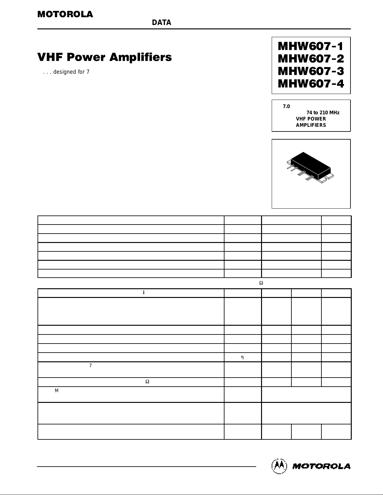
. . . designed for 7.5 volt VHF power amplifier applications in industrial and
commercial equipment primarily hand portable radios.
• MHW607–1: 136–150 MHz
• MHW607–2: 146–174 MHz
• MHW607–3: 174–195 MHz
• MHW607–4: 184–210 MHz
• Specified 7.5 Volt Characteristics:
— RF Input Power = 1.0 mW (0 dBm)
— RF Output Power = 7.0 Watts (MHW607–1,–2); 6.5 W (MHW607–3,–4)
— Minimum Gain (V
Control
= 7.0 V) = 38.5 dB
— Harmonics = –40 dBc Max @ 2.0 f
o
• 50 Ω Input/Output Impedance
• Guaranteed Stability and Ruggedness
• Epoxy Glass PCB Construction Gives Consistent Performance and Reliability
• Circuit board photomaster available upon request by contacting RF Tactical
Marketing in Phoenix, AZ.
MAXIMUM RATINGS (Flange Temperature = 25°C)
Rating Symbol Value Unit
DC Supply Voltage (Pins 2, 4, 5) V
s1,2,3
9.0 Vdc
DC Control Voltage (Pin 3) V
Cont
9.0 Vdc
RF Input Power P
in
5.0 mW
RF Output Power (Vs1 = Vs2 = Vs3 = 9.0 V) P
out
10 W
Operating Case Temperature Range T
C
–30 to +100 °C
Storage Temperature Range T
stg
–30 to +100 °C
ELECTRICAL CHARACTERISTICS (V
s1
= Vs2 = Vs3 = 7.5 Vdc, (Pins 2, 4, 5), TC = 25°C, 50 W System)
Characteristic
Symbol Min Max Unit
Frequency Range MHW607–1
MHW607–2
MHW607–3
MHW607–4
— 136
146
174
184
150
174
195
210
MHz
Control Voltage (P
out
= 7.0 W, Pin = 1.0 MW)
(1)
V
Cont
0 7.0 Vdc
Quiescent Current (Vs1 = Vs2 = Vs3 = 7.5 Vdc, V
Cont
= 7.0 Vdc) I
s1(q)
+ I
s2(q)
— 160 mA
Power Gain (P
out
= 7.0 W, V
Cont
= 7.0 Vdc) G
p
38.5 — dB
Efficiency (P
out
= 7.0 W, Pin = 1.0 mW)
(1)
h
40 — %
Harmonics (P
out
= 7.0 W)
(1) 2 f
o
(Pin = 1.0 mW) 3 f
o
— — –40
–45
dBc
Input VSWR (P
out
= 7.0 W, Pin = 1.0 mW), 50 W Ref. (1)
— — 2.0:1 —
Load Mismatch (Vs1 = Vs2 = Vs3 = 9.0 Vdc)
VSWR = 20:1, P
out
= 8 W, Pin = 5.0 mW)
(1)
No Degradation
in Power Output
Stability (Pin = 1.0–30 mW, Vs1 = Vs2 = Vs3 = 6.0–9.0 Vdc)
P
out
between 1.0 W and 10 W
(1)
Load VSWR = 8:1
All spurious outputs
more than 60 dB
below desired signal
Control Current (Vs1 = Vs2 = Vs3 = 7.5 V,
Pin = 0 dBm, V
Cont
Set for Po = 7.0 W)
— 325 mA
(1) Adjust V
Cont
for specified P
out
.
Order this document
by MHW607/D
SEMICONDUCTOR TECHNICAL DATA
7.0 W — 136 to 210 MHz
6.5 W — 174 to 210 MHz
VHF POWER
AMPLIFIERS
CASE 301K–02, STYLE 3
Motorola, Inc. 1994
REV 6
Page 2
MHW607–1 MHW607–2 MHW607–3 MHW607–4
2
MOTOROLA RF DEVICE DATA
1
PIN
NO.
C10 C4
L3
C5
R.F.
OUT
Z2
C7
L4L2
543
6
2
C9
C6
C3
L1
C2
C8
Z1
C1
R.F.
IN
SIGNAL
GENERATOR
10 dB
ATTENUATOR
C1 — 0.018
m
F Chip
C2, C3, C4, C5, C6, C7, C8 — 0.018
m
F Chip
C9, C10 — 3.3
m
F Tantalum
L1, L2, L3, L4 — 0.2
m
H
Z1, Z2 — 50
W
Microstrip
V
CONTROL
+7.0 Vdc
@ 250 mA
(TYPICAL)
Vs1, V
s2
+7.5 Vdc
@ 145 mA
(TYPICAL)
V
s3
+7.5 Vdc
@ 1.75 A
(TYPICAL)
50
OHM
LOAD
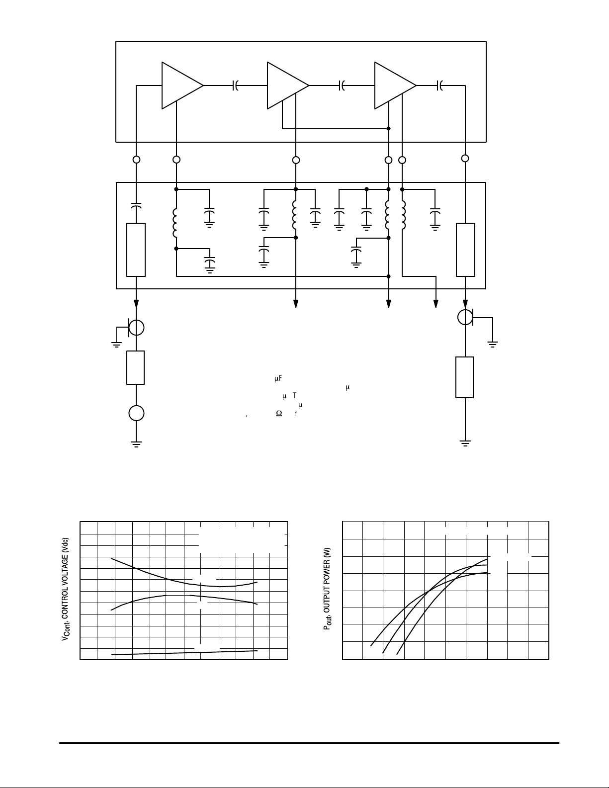
Figure 1. Power Module Test
System Block Diagram
TYPICAL CHARACTERISTICS
f, FREQUENCY (MHz)
η
V
Cont
2
150
6
5
4
180170140
1
3
160
VSWR
50
45
40
1.2:1
1.1:1
1.0:1
Pin = 1 mW
P
out
= 7 W
Vs1 = Vs2 = Vs3 = 7.5 Vdc
VSWR EFFICIENCY (%)
V
Cont
, CONTROL VOLTAGE (Vdc)
Vs1 = Vs2 = Vs3 = 7.5 V
2
31 4 5 6 7 8 9 10
4
6
8
10
12
14
155
2
174
f = 146 MHz
Figure 2. Control Voltage, Efficiency and VSWR
versus Frequency
Figure 3. Output Power versus Control Voltage
Page 3
3
MHW607–1 MHW607–2 MHW607–3 MHW607–4MOTOROLA RF DEVICE DATA
TYPICAL CHARACTERISTICS
6
4
8
10
12
14
170 180
16
160
Vs1 = Vs2 = Vs3 = 7.5 Vdc
Pin = 1 mW
VC = 7 V
140
2
f, FREQUENCY (MHz)
Vs1 = Vs2 = Vs3 = 6 Vdc
190150
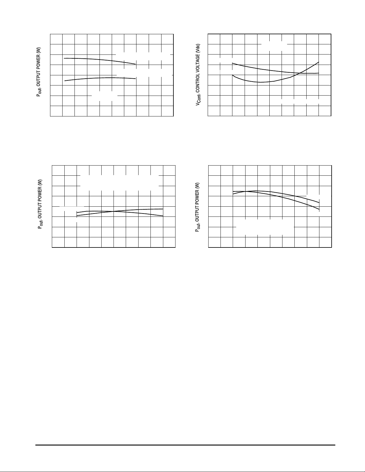
Figure 4. Output Power versus Frequency
Vs1 = Vs2 = Vs3 = 7.5 Vdc
174 MHz
Pin = 1 mW
P
out
= 7 W
f = 146 MHz
1
3
5
7
2
4
6
8
–60 20 60–40 0 40–20 10080–80
TC, CASE TEMPERATURE (
°
C)
Figure 5. Control Voltage versus Case Temperature
6
4
8
10
12
14
2
Pin = 1 mW
Vs1 = Vs2 = Vs3 = 7.5 Vdc
V
Cont
SET FOR P
out
= 7 W @ TC = 20
°
C
146 MHz
f = 174 MHz
–60 20 60–40 0 40–20 10080–80
TC, CASE TEMPERATURE (
°
C)
Figure 6. Output Power versus Case Temperature
6
4
8
10
12
14
2
174 MHz
f = 146 MHz
Pin = 1 mW
Vs1 = Vs2 = Vs3 = 7.5 Vdc
V
Cont
= 7 Vdc
–60 20 60–40 0 40–20 10080–80
TC, CASE TEMPERATURE (
°
C)
Figure 7. Output Power versus Case Temperature
at Maximum Control Voltage
Page 4

MHW607–1 MHW607–2 MHW607–3 MHW607–4
4
MOTOROLA RF DEVICE DATA
APPLICATIONS INFORMATION
NOMINAL OPERATION
All electrical specifications are based on t he nominal
conditions of Vs1 = Vs2 = Vs3 = 7.5 Vdc (Pins 2, 4, 5) and P
out
equal to 7.0 watts. With these conditions, maximum current
density on any device is 1.5 x 10⁵ A/cm2 and maximum die
temperature with 100°C case operating temperature is
165°C. While the modules are designed to have excess gain
margin with ruggedness, operation of these units outside the
limits of published specifications is not recommended unless
prior c ommunications regarding intended use have been
made with the factory representative.
GAIN CONTROL
The module output should be limited to 7.0 watts. The pre-
ferred method of power output control is to fix Vs1 = Vs2 = V
s3
= 7.5 Vdc (Pins 2, 4, 5), Pin (Pin 1) at 1.0 mW, and vary V
Cont
(Pin 3) voltage.
DECOUPLING
Due to the high gain of the three stages and the module
size limitation, external decoupling networks require careful
consideration. Pins 2, 3, 4 and 5 are internally bypassed with
a 0.018 µF chip capacitor which is effective for frequencies
from 5.0 MHz through 174 MHz. For bypassing frequencies
below 5.0 MHz, networks equivalent to that shown in Figure
1 are recommended. Inadequate decoupling will result in
spurious outputs at certain operating frequencies and certain
phase angles of input and output VSWR.
LOAD MISMATCH
During final test, each module is load mismatch tested in a
fixture having the identical decoupling networks described in
Figure 1. Electrical conditions are Vs1 = Vs2 = Vs3 equal to
9.0 Vdc, VSWR equal to 20:1, and output power equal to 8.0
watts.
Page 5
5
MHW607–1 MHW607–2 MHW607–3 MHW607–4MOTOROLA RF DEVICE DATA
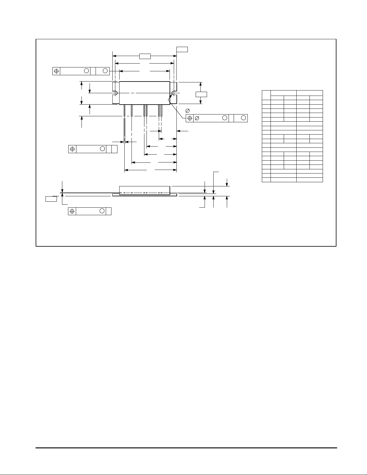
PACKAGE DIMENSIONS
CASE 301K–02
ISSUE G
NOTES:
1. DIMENSIONING AND TOLERANCING PER ANSI
Y14.5M, 1982.
2. CONTROLLING DIMENSION: INCH.
3. DIMENSION F TO CENTER OF LEADS.
STYLE 3:
PIN 1. RF INPUT
2. VS1
3. VCONT
4. VS2
5. VS3
6. RF OUTPUT
CASE: GROUND
6 PLP
M
0.25 (0.010) T
E
F
C
SEATING
PLANE
–T–
DIM MIN MAX MIN MAX
MILLIMETERSINCHES
A 1.770 1.785 44.96 45.35
B 1.370 1.390 34.80 35.31
C 0.250 0.265 6.35 6.73
D 0.018 0.022 0.46 0.55
E 0.085 0.100 2.16 2.54
F 0.132 BSC 3.35 BSC
G 1.655 BSC 42.04 BSC
H 1.490 BSC 37.85 BSC
J 0.267 0.278 6.78 7.06
K 0.230 0.300 5.85 7.62
L 0.990 BSC 25.15 BSC
N 1.290 BSC 32.77 BSC
P 0.008 0.012 0.21 0.30
Q 0.120 0.130 3.05 3.30
R 0.535 0.555 13.59 14.09
S 0.445 0.465 11.31 11.81
V 0.890 BSC 22.61 BSC
W 0.285 BSC 7.24 BSC
X 0.390 BSC 9.91 BSC
B
G
6 PL
J
K
R
–A–
–Z–
D
2 PLQ
Z
M
0.25 (0.010) T
M
A
M
0.13 (0.005) T
1 2 3 4 5
H
N
L
–S–
V
X
W
6
M
S
M
0.13 (0.005) T
Page 6

MHW607–1 MHW607–2 MHW607–3 MHW607–4
6
MOTOROLA RF DEVICE DATA
Motorola reserves the right to make changes without further notice to any products herein. Motorola makes no warranty , representation or guarantee regarding
the suitability of its products for any particular purpose, nor does Motorola assume any liability arising out of the application or use of any product or circuit,
and specifically disclaims any and all liability, including without limitation consequential or incidental damages. “T ypical” parameters can and do vary in different
applications. All operating parameters, including “T ypicals” must be validated for each customer application by customer’s technical experts. Motorola does
not convey any license under its patent rights nor the rights of others. Motorola products are not designed, intended, or authorized for use as components in
systems intended for surgical implant into the body, or other applications intended to support or sustain life, or for any other application in which the failure of
the Motorola product could create a situation where personal injury or death may occur. Should Buyer purchase or use Motorola products for any such
unintended or unauthorized application, Buyer shall indemnify and hold Motorola and its officers, employees, subsidiaries, affiliates, and distributors harmless
against all claims, costs, damages, and expenses, and reasonable attorney fees arising out of, directly or indirectly, any claim of personal injury or death
associated with such unintended or unauthorized use, even if such claim alleges that Motorola was negligent regarding the design or manufacture of the part.
Motorola and are registered trademarks of Motorola, Inc. Motorola, Inc. is an Equal Opportunity/Affirmative Action Employer.
How to reach us:
USA /EUROPE: Motorola Literature Distribution; JAPAN: Nippon Motorola Ltd.; Tatsumi–SPD–JLDC, Toshikatsu Otsuki,
P.O. Box 20912; Phoenix, Arizona 85036. 1–800–441–2447 6F Seibu–Butsuryu–Center, 3–14–2 Tatsumi Koto–Ku, Tokyo 135, Japan. 03–3521–8315
MFAX: [email protected] – TOUCHTONE (602) 244–6609 HONG KONG: Motorola Semiconductors H.K. Ltd.; 8B Tai Ping Industrial Park,
INTERNET: http://Design–NET.com 51 Ting Kok Road, Tai Po, N.T., Hong Kong. 852–26629298
MHW607/D
*MHW607/D*
◊
 Loading...