

Page 1
1
MHW5182AMOTOROLA RF DEVICE DATA
The RF Line
. . . designed specifically for 450 MHz CATV applications. Features ion–implanted arsenic emitter transistors with 7.0 GHz fT and an all gold metallization
system.
• Specified for 53– and 60–Channel Performance
• Broadband Power Gain @ f = 40–450 MHz
Gp = 18.2 dB (Typ) @ 50 MHz
19.0 dB (Typ) @ 450 MHz
• Broadband Noise Figure
NF = 6.5 dB (Max)
• Superior Gain, Return Loss and DC Current Stability with Temperature
• All Gold Metallization
• 7.0 GHz Ion–Implanted Transistors
ABSOLUTE MAXIMUM RATINGS
Rating Symbol Value Unit
RF Voltage Input (Single Tone) V
in
+70 dBmV
DC Supply Voltage V
CC
+28 Vdc
Operating Case Temperature Range T
C
–20 to +100 °C
Storage Temperature Range T
stg
–40 to +100 °C
ELECTRICAL CHARACTERISTICS (V
CC
= 24 Vdc, TC = +30°C, 75 Ω system unless otherwise noted)
Characteristic
Symbol Min Typ Max Unit
Frequency Range BW 40 — 450 MHz
Power Gain — 50 MHz G
p
17.8 18.2 18.8 dB
Power Gain — 450 MHz G
p
18.5 19 20 dB
Slope S 0.3 — 1.5 dB
Gain Flatness (Peak To Valley) — — 0.2 0.4 dB
Return Loss — Input/Output 40–450 MHz
(Zo = 75 Ohms)
IRL/ORL 18 — — dB
Second Order Intermodulation Distortion
(V
out
= +46 dBmV per ch., Ch 2, M6, M15)
(V
out
= +46 dBmV per ch., Ch 2, M13, M22)
IMD
—
—
–85
–80
—
–72
dB
Cross Modulation Distortion 53–Channel FLAT
(V
out
= +46 dBmV per ch.) 60–Channel FLAT
XMD
53
XMD
60
—
—
–62
–61
—
–59
dB
Composite Triple Beat 53–Channel FLAT
(V
out
= +46 dBmV per ch.) 60–Channel FLAT
CTB
53
CTB
60
—
—
–64
–62
—
–61
dB
DIN (European Applications Only)*
300 MHz — (CH V + Q – P @ W)
400 MHz— (CH M8 + M15 – M9 @ M14)
450 MHz — (CH M20 + M23 – M22 @ M21)
DIN1
DIN2
DIN3
—
—
—
126
126
125
—
—
—
dBµV**
Noise Figure (f = 450 MHz) NF — 5.5 6.5 dB
DC Current I
DC
— 210 240 mA
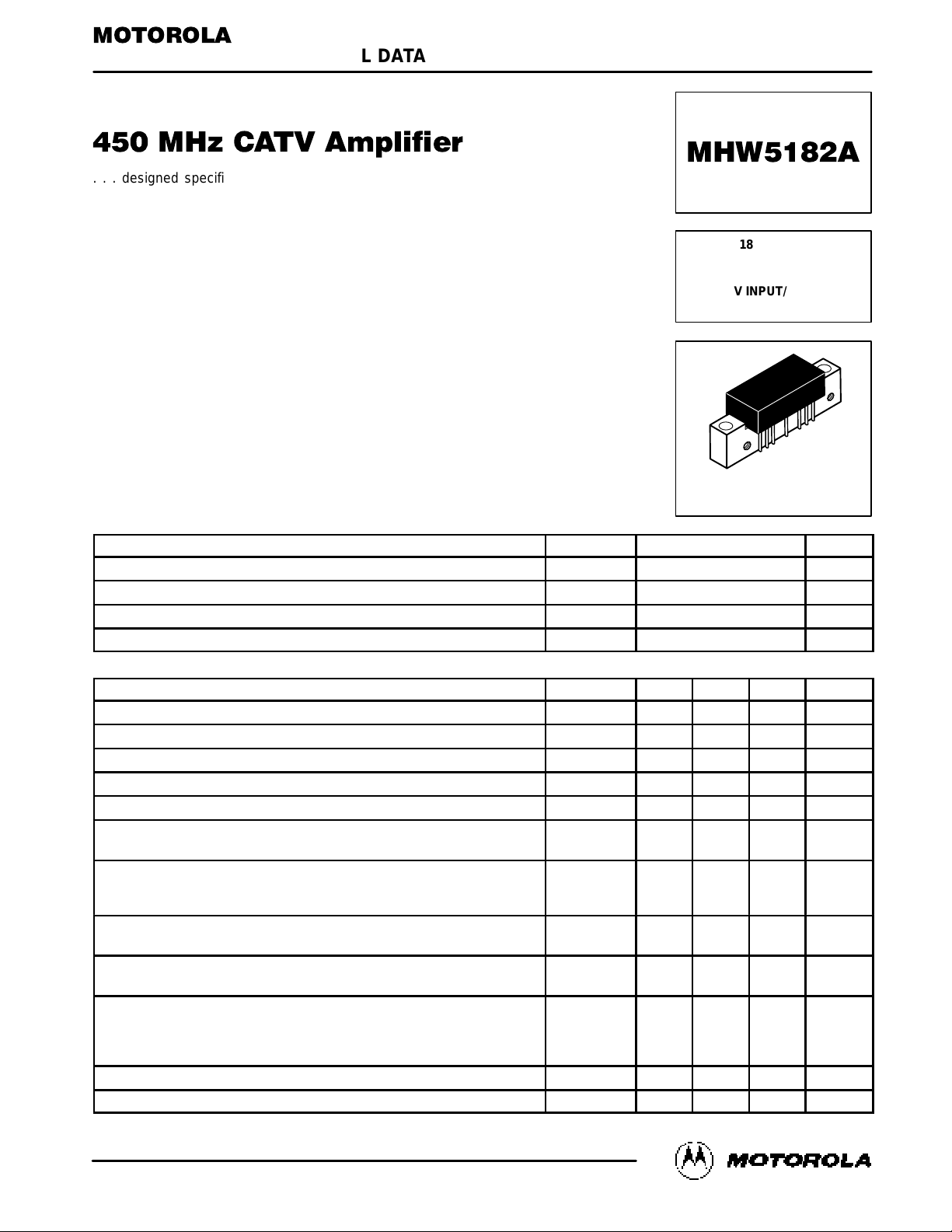
Order this document
by MHW5182A/D
SEMICONDUCTOR TECHNICAL DATA
18 dB GAIN
450 MHz
60–CHANNEL
CATV INPUT/OUTPUT
TRUNK AMPLIFIER
CASE 714–06, STYLE 1
Motorola, Inc. 1994
Page 2
MHW5182A
2
MOTOROLA RF DEVICE DATA
*DIN (European Applications Only)
NCTA Channel
Designation
Frequency
(MHz)
DIN Output Level
(dBmV)**(Typ)
DIN Beat Level
dB Relative to Ref. Ch.
P
Q
V
W (Ref.)
253.25
259.25
289.25
295.25
+60
+60
+66
+66
¬
–60
M8
M9
M14 (Ref.)
M15
361.25
367.25
397.25
403.25
+60
+60
+66
+66
¬
–60
M20
M21 (Ref.)
M22
M23
433.25
439.25
445.25
451.25
+65
+65
+59
+59
¬
–60
**DIN (dBmV) = Reference Channel Level (dBmV) +60 dB
Page 3

3
MHW5182AMOTOROLA RF DEVICE DATA
PACKAGE DIMENSIONS
CASE 714–06
ISSUE K
NOTES:
1. DIMENSIONING AND TOLERANCING PER ANSI
Y14.5M, 1982.
2. CONTROLLING DIMENSION: INCH.
STYLE 1:
PIN 1. RF INPUT
2. GROUND
3. GROUND
4. DELETED
5. VDC
6. DELETED
7. GROUND
8. GROUND
9. RF OUTPUT
DIM MIN MAX MIN MAX
MILLIMETERSINCHES
A ––– 1.775 ––– 45.08
B ––– 1.085 ––– 27.56
C ––– 0.840 ––– 21.34
D 0.018 0.022 0.46 0.56
E 0.465 0.510 11.81 12.95
F 0.300 0.325 7.62 8.25
G 0.100 BSC 2.54 BSC
J 0.156 BSC 3.96 BSC
K 0.315 0.355 8.00 8.50
L 1.00 BSC 25.40 BSC
N 0.165 BSC 4.10 BSC
P 0.100 BSC 2.54 BSC
Q 0.148 0.168 3.76 4.27
R ––– 0.595 ––– 15.11
S 1.500 BSC 38.10 BSC
U 0.200 BSC 5.08 BSC
V 0.280 BSC 7.11 BSC
W 0.435 0.450 11.05 11.43
–A–
–Z–
–F–
B
S
V
R
Q
M
F
M
0.25 (0.010) A
M
T
T
M
0.25 (0.010) A
M
Z
2 PL
T
M
0.25 (0.010) A
M
D
7 PL
C
P
K
W
U
N
G
L
–E–
–T–
6–32UNC–2B
2 PL
1 2 3 5 7 8 9
J
Motorola reserves the right to make changes without further notice to any products herein. Motorola makes no warranty, representation or guarantee regarding
the suitability of its products for any particular purpose, nor does Motorola assume any liability arising out of the application or use of any product or circuit,
and specifically disclaims any and all liability, including without limitation consequential or incidental damages. “T ypical” parameters can and do vary in different
applications. All operating parameters, including “T ypicals” must be validated for each customer application by customer’s technical experts. Motorola does
not convey any license under its patent rights nor the rights of others. Motorola products are not designed, intended, or authorized for use as components in
systems intended for surgical implant into the body, or other applications intended to support or sustain life, or for any other application in which the failure of
the Motorola product could create a situation where personal injury or death may occur. Should Buyer purchase or use Motorola products for any such
unintended or unauthorized application, Buyer shall indemnify and hold Motorola and its officers, employees, subsidiaries, affiliates, and distributors harmless
against all claims, costs, damages, and expenses, and reasonable attorney fees arising out of, directly or indirectly, any claim of personal injury or death
associated with such unintended or unauthorized use, even if such claim alleges that Motorola was negligent regarding the design or manufacture of the part.
Motorola and are registered trademarks of Motorola, Inc. Motorola, Inc. is an Equal Opportunity/Affirmative Action Employer.
Page 4

MHW5182A
4
MOTOROLA RF DEVICE DATA
Literature Distribution Centers:
USA: Motorola Literature Distribution; P.O. Box 20912; Phoenix, Arizona 85036.
EUROPE: Motorola Ltd.; European Literature Centre; 88 T anners Drive, Blakelands, Milton Keynes, MK14 5BP, England.
JAPAN: Nippon Motorola Ltd.; 4-32-1, Nishi-Gotanda, Shinagawa-ku, Tokyo 141, Japan.
ASIA PACIFIC: Motorola Semiconductors H.K. Ltd.; Silicon Harbour Center, No. 2 Dai King Street, Tai Po Industrial Estate, Tai Po, N.T., Hong Kong.
MHW5182A/D
*MHW5182A/D*
◊
 Loading...