

Page 1
Advance Information
UHF Silicon FET
Power Amplifier
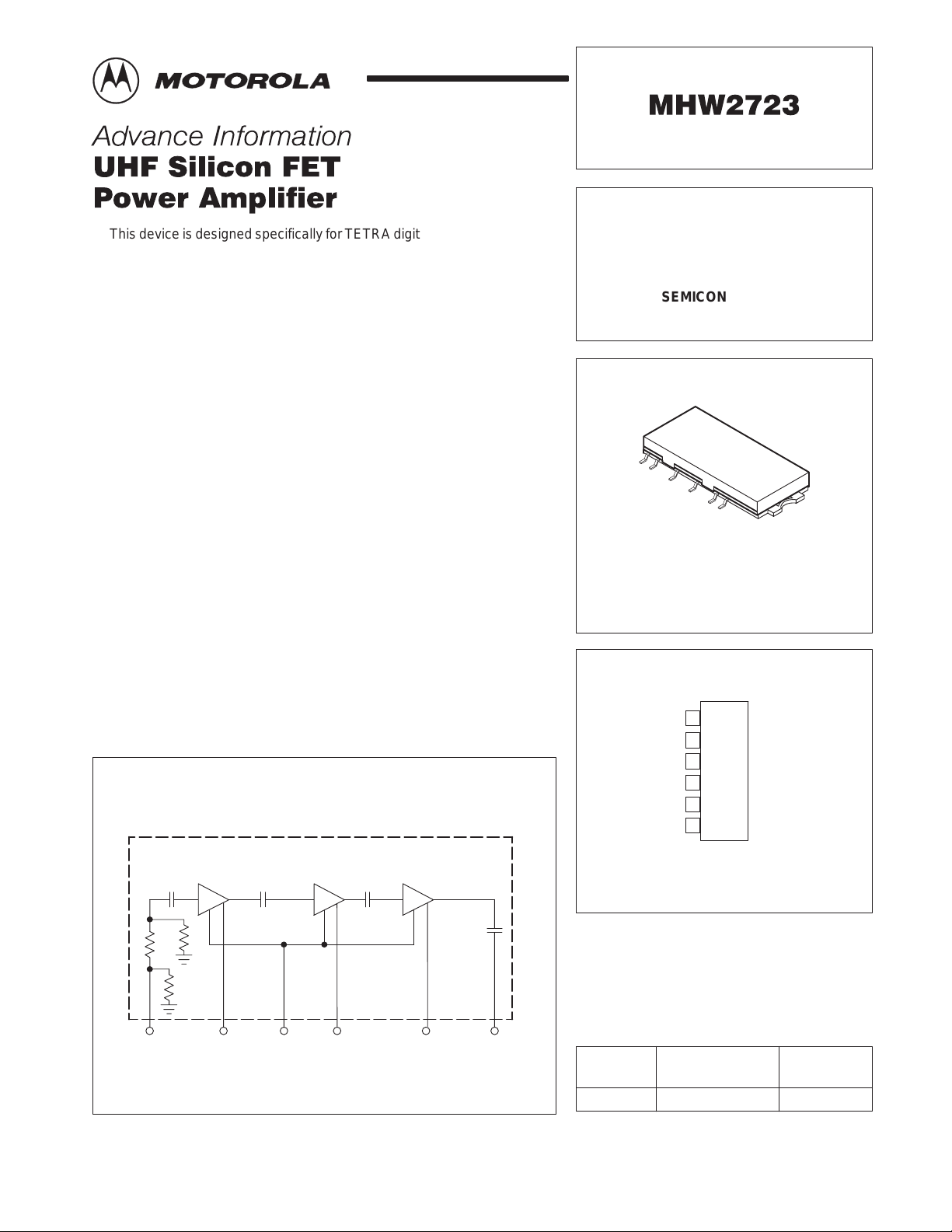
This device is designed specifically for TETRA digital 3.0 W mobile radios,
operates from a 12.5 V supply and features 28 dB minimum gain.
• Specified 12.5 V Characteristics:
RF Input Power: 9.0 dBm
RF Output Power: 5.0 W
Power Gain: 28 dB Min
Harmonics: –30 dBc Max @ 2
• Metal Case Low Profile Gives Consistent Performance and Reliability
• 50 Ω Input/Output Impedances
• Guaranteed Stability and Ruggedness
f
o
Order this document by MHW2723/D
MHW2723
UHF POWER AMPLIFIER
5.0 W, 380 to 470 MHz
SEMICONDUCTOR
TECHNICAL DATA
1
Simplified Block Diagram
6
CASE 420Z
PIN CONNECTIONS
P
1
in
V
2
S2
V
3
bias
V
4
S4
V
5
S5
6P
out
(Top View)
1
This document contains information on a new product. Specifications and information herein
are subject to change without notice.
MOTOROLA RF/IF DEVICE DATA
2456
This device contains 3 active transistors.
3
ORDERING INFORMATION
Operating
Device
MHW2723 TC = –30 to 90°C Power Module
Motorola, Inc. 1998 Rev 0
Temperature Range
Package
1
Page 2
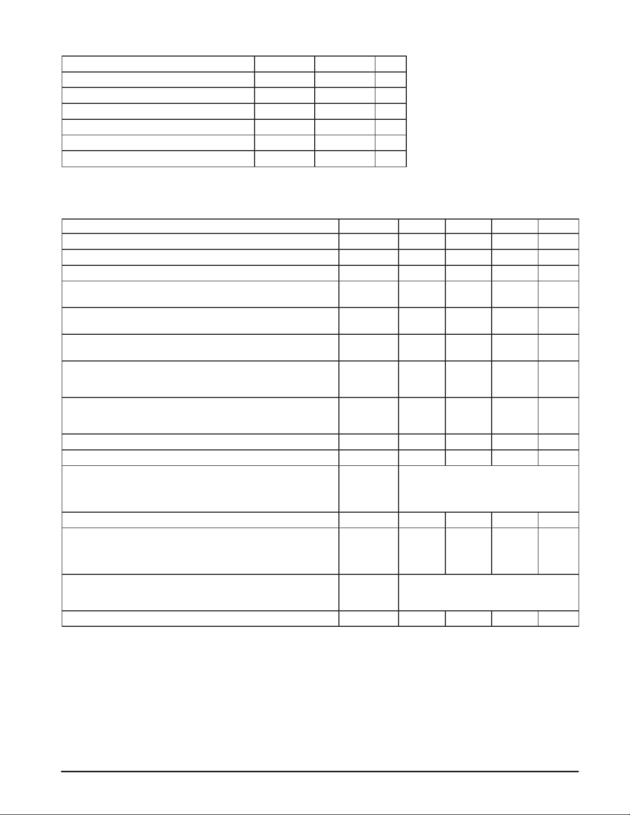
MAXIMUM RATINGS
DC Supply Voltage (Pins 2, 4, 5) V
DC Bias Voltage (Pin 3) V
RF Input Power P
RF Output Power (V
Operating Case Temperature Range T
Storage Temperature Range T
NOTES: 1. Meets Human Body Model (HBM) ≤3000 V .
2.ESD data available upon request.
(TC = 25°C, unless otherwise noted.)
Rating Symbol Value Unit
= 16 V) P
S2, 4, 5
MHW2723
S2, 4, 5
bias
in
out
C
stg
16 Vdc
5.0 Vdc
14 dBm
12 W
–30 to 90 °C
–30 to 100 °C
ELECTRICAL CHARACTERISTICS (V
Characteristic
Frequency Range BW 380 – 470 MHz
RF Input Power Range P
Saturated Output Power (Pin = 14 dBm) (Note 1) P
Power Gain
(Adjust Pin for P
Input Return Loss
(Pin = –8 to 14 dBm: 50 Ω Ref.)
Efficiency
(P
= 5.0 W)
out
Adjacent Channel Power
(P
= 5.0 W; f = fo ± 25 KHz, 18 KHz Bandwidth, π/4 DQPSK
out
Modulation 36 KBITS/S, On/Off Factor 0.35) (Note 2)
Alternate Channel Power
(P
= 5.0 W; f = fo ± 50 KHz, 18 KHz Bandwidth, π/4 DQPSK
out
Modulation 36 KBITS/S, On/Off Factor 0.35) (Note 2)
Bias Current (V
Rise Time (P
Stability
(P
V
S2, 4, 5
All Phase Angles at Frequency of Test)
Harmonics (P
Isolation
(V
V
S2, 4, 5
Source Impedance = 50 Ω)
Load Mismatch Stress (V
(25% Duty Cycle Period = 56.7 ms); Load VSWR = 2:1,
All Phase Angles at Frequency of Test) (Note 1)
Noise Power (P
NOTES: 1. Pulsed V
out
= –20 dBm Avg to 38 dBm Avg; V
out
= 10.8–16 Vdc; Load VSWR = 2:1, Source VSWR = 2:1,
= 0 V; Pin = Nominal Drive Level for P
bias
= 12.5 Vdc; Case Temperature = 25°C; Load Impedance and
2.TETRA Signal Format – Continuous Wave.
= 5.0 W)
out
= 4.5 V) I
bias
= 0.1 mW to 12 W) (Note 1) t
= 5.0 W) 2 f
out
= 5.0 W; f = fo + 5.0 MHz; Bandwidth = 18 KHz) P
out
or Pin; Duty Cycle = 25%, Period = 56.7 ms: On Time = 14.17 ms.
bias
o
S2, 4, 5
= 16 Vdc; V
= 4.5 V; V
bias
= 4.5 V Pulse Pin;
bias
= 12 W;
out
= 4.5 V; Pin = 12 dBm;
bias
= 12.5 Vdc; TC = 25°C, 50 Ω system, unless otherwise noted)
S2, 4, 5
Symbol Min Typ Max Unit
in
sat
G
p
VSWR
in
η 18 – – %
ACP –30 – – dBc
ACP –40 – – dBc
bias
r
–
– – – –30 dBc
– – – 60 dB
ψ
N
–8.0 – 14 dBm
12 – – W
28 – – dB
– – 2:1 –
– – 10 mA
– – 20 µsec
All Spurious Outputs
More Than 60 dB
Below Desired Signal
No Degradation in Output
Power Before & After Test
– – –85 dBm
2
MOTOROLA RF/IF DEVICE DATA
Page 3
MHW2723
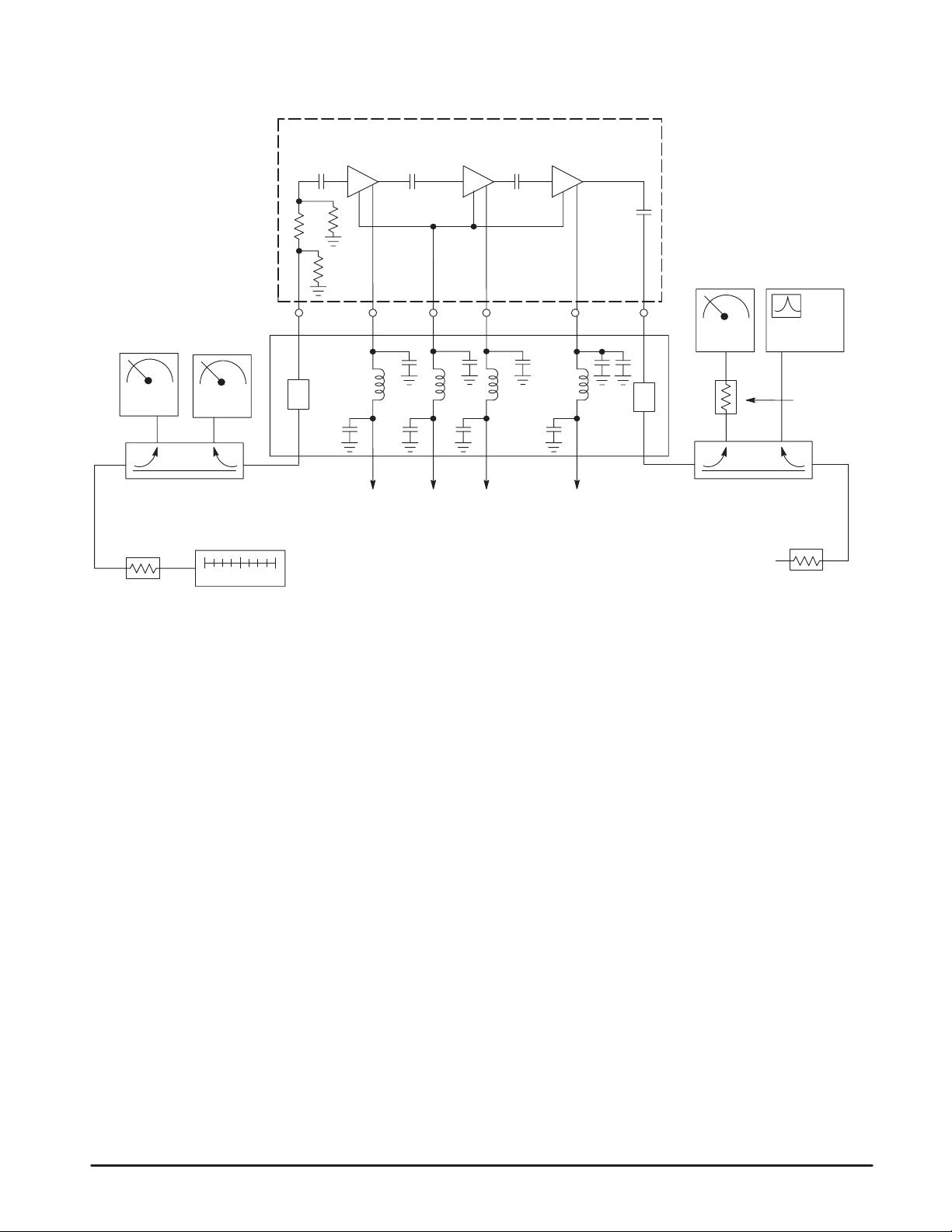
Figure 1. T est Circuit Diagram
Block Diagram
Input
Power
Meter
20 dB Dual
Directional Coupler
10 dB
Minimum
Attenuation
Reflected
Power
Meter
RF Signal
Generator
1
RF In
Output
Power
Meter
2456
Z
1
C1
V
S2
12.5 V
3
L1 L2 L3 L4
C3 C5 C7
V
bias
4.5 V
L1 – L4 = 0.22 µH Choke Coil
C1, C3, C4,
C5, C7, C9 = 0.018 µF Chip Cap
C2, C6 = 0.1 µF Chip Cap
C8 = 3.3 µF Chip Cap
Z1, Z2 = 50 Ω Microstrip
V
S4
12.5 V
Test Fixture
V
S5
12.5 V
C9
C8C6C4C2
Z
2
RF Out
Directional Coupler
Spectrum
Analyzer
20 dB
Attenuator
20 dB Dual
Power
T ermination
MOTOROLA RF/IF DEVICE DATA
3
Page 4
MHW2723
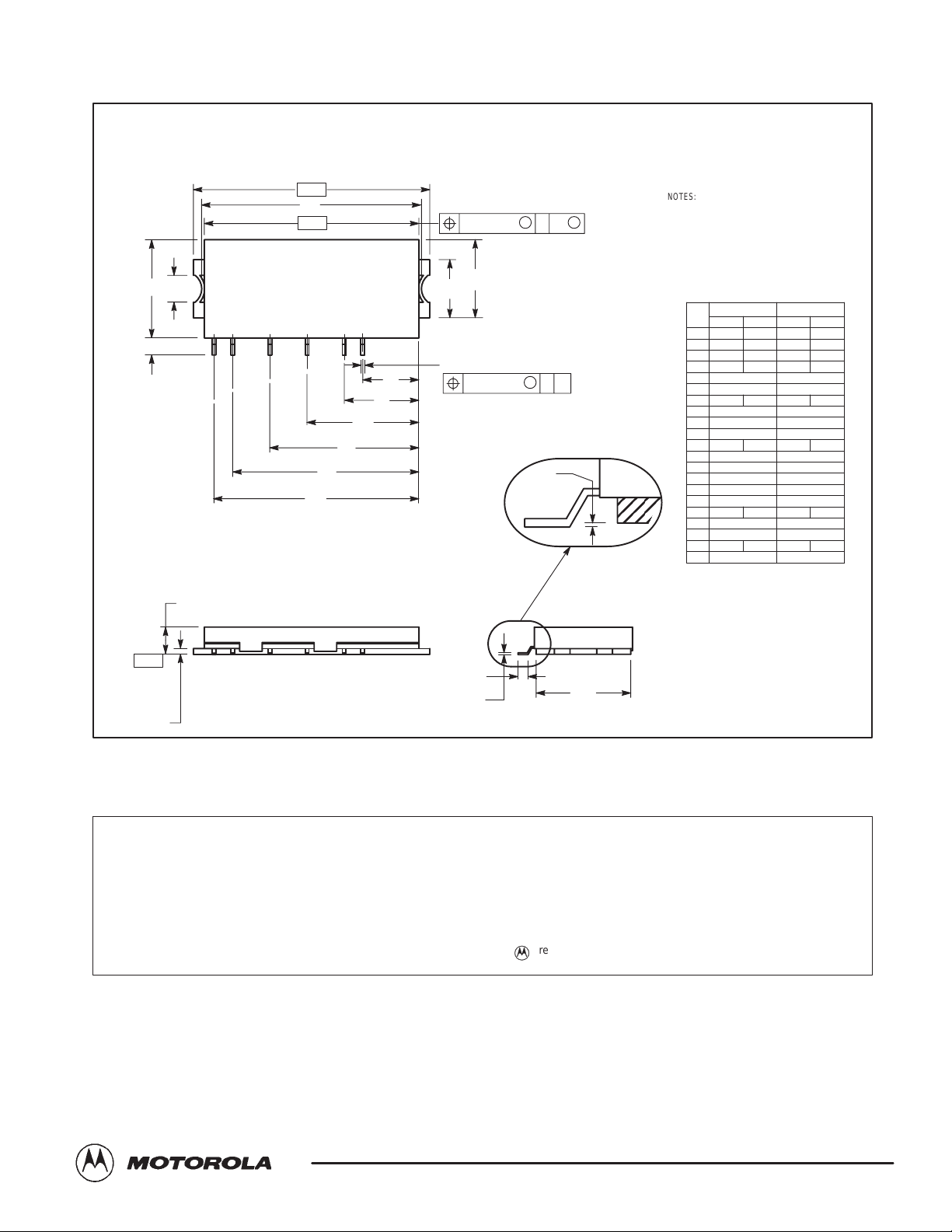
OUTLINE DIMENSIONS
POWER MODULE
CASE 420Z–02
ISSUE A
–A–
G
–B–
R
Q
12 3 4 56
0.25 (0.010)MTA
AC
S
L
K
D 6 PL
X
0.64 (0.025)MTB
Y
V
N
H
W
AE
NOTE 3
NOTES:
1. DIMENSIONING AND TOLERANCING PER ANSI
Y14.5M, 1982.
2. CONTROLLING DIMENSION: MILLIMETER.
3. DIMENSION AE (PACKAGE COPLANARITY):
THE BOTTOM OF THE DEVICE LEADS AND THE
REFERENCE PLANE –T– MUST BE COPLANAR
WITHIN DIMENSION AE.
4. REF INDICATES NON–CONTROLLED DIMENSION
FOR REFERENCE USE ONLY.
DIM MIN MAX MIN MAX
A 31.75 32.05 1.250 1.262
B 28.80 29.10 1.134 1.146
C 3.70 4.00 0.146 0.157
D 0.43 0.58 0.017 0.023
G 29.60 REF 1.165 REF
H 25.03 BSC 0.985 BSC
K 2.10 2.62 0.083 0.103
N 20.03 BSC 0.789 BSC
P 0.25 REF 0.010 REF
Q 3.78 REF 0.149 REF
R 13.06 13.45 0.514 0.530
S 8.00 REF 0.315 REF
V 15.03 BSC 0.592 BSC
W 27.53 BSC 1.084 BSC
X 7.53 BSC 0.297 BSC
Y 10.03 BSC 0.395 BSC
AA
1.35 1.70
AC 10.50 REF 0.413 REF
AD 0.81 REF 0.032 REF
AE +0.050 –0.076 +0.002 –0.003
AF 12.80 REF 0.504 REF
INCHESMILLIMETERS
0.053 0.067
C
–T–
P 6 PL
AA
AF
SEATING
PLANE
AD
Motorola reserves the right to make changes without further notice to any products herein. Motorola makes no warranty , representation or guarantee regarding
the suitability of its products for any particular purpose, nor does Motorola assume any liability arising out of the application or use of any product or circuit, and
specifically disclaims any and all liability, including without limitation consequential or incidental damages. “T ypical” parameters which may be provided in Motorola
data sheets and/or specifications can and do vary in different applications and actual performance may vary over time. All operating parameters, including “Typicals”
must be validated for each customer application by customer’s technical experts. Motorola does not convey any license under its patent rights nor the rights of
others. Motorola products are not designed, intended, or authorized for use as components in systems intended for surgical implant into the body, or other
applications intended to support or sustain life, or for any other application in which the failure of the Motorola product could create a situation where personal injury
or death may occur. Should Buyer purchase or use Motorola products for any such unintended or unauthorized application, Buyer shall indemnify and hold Motorola
and its officers, employees, subsidiaries, affiliates, and distributors harmless against all claims, costs, damages, and expenses, and reasonable attorney fees
arising out of, directly or indirectly, any claim of personal injury or death associated with such unintended or unauthorized use, even if such claim alleges that
Motorola was negligent regarding the design or manufacture of the part. Motorola and are registered trademarks of Motorola, Inc. Motorola, Inc. is an Equal
Opportunity/Affirmative Action Employer.
How to reach us:
USA/EUROPE/Locations Not Listed: Motorola Literature Distribution; JAPAN: Nippon Motorola Ltd.; SPD, Strategic Planning Office, 141,
P.O. Box 5405, Denver, Colorado 80217. 1–303–675–2140 or 1–800–441–2447 4–32–1 Nishi–Gotanda, Shinagawa–ku, Tokyo, Japan. 81–3–5487–8488
Customer Focus Center: 1–800–521–6274
Mfax: [email protected] – TOUCHTONE 1–602–244–6609 ASIA/PACIFIC: Motorola Semiconductors H.K. Ltd.; 8B Tai Ping Industrial Park,
Moto rola Fax Back System – US & Canada ONLY 1–800–774–1848 51 Ting Kok Road, Tai Po, N.T., Hong Kong. 852–26629298
– http://sps.motorola.com/mfax/
HOME PAGE: http://motorola.com/sps/
Mfax is a trademark of Motorola, Inc.
4
◊
MOTOROLA RF/IF DEVICE DATA
MHW2723/D
 Loading...