

Page 1
MH89770
T1/ESF Framer & Interface
Preliminary Information
Features
• Complet e interfac e to a bi direct iona l T1 link
• D3/D4 or ESF frami ng and S LC-96 com patib le
• Two frame elastic buffer with jitter tolerance
improved t o 156UI
• Insertion and dete ction of A, B, C, D bits
Signalling freeze , opt iona l debo unc e
• Selectable B8ZS, jammed bit (ZCS) or no zero
code suppression
• Yellow and blue al arm si gnal ca pabil ities
• Bipolar violation count, F
error count
• Frame and superframe sync. signals, Tx and Rx
• Per channel, overall, and remote loop around
• 8 kHz synchronization output
• Digital ph ase det ecto r betw een T1 line and
ST-BUS
• ST-BUS compatible
• Pin compatible with the MH89760BN/BS
• Inductorless clock recovery
• Loss of Sign al (LO S) indi cation
• Available in standard, narrow and surface
mount form ats
error count, CRC
T
ISSUE 2 March 1995
Ordering Information
MH89770N 40 Pin DIL Hybrid 0.8" row pitch
MH89770S 40 Pin Surface Mount Hybrid
0°C to 70°C
Applications
• DS1/ESF di gital trun k in terface s
• Computer to PBX interfaces (DMI and CPI)
• High speed computer to computer data links
Description
The MH89770 is a complete T1 interface solution,
meeting the Extended Super Frame (ESF), D3/D4
and SLC-96 formats. The MH89770 interfaces to the
DS1 1.544 Mbit/sec digital trunk and has the
capability of meeting ACCUNET
tole ran c e (13 8 UI ).
The MH89770 is a pin-compatible enhancement of
the MH89760B.
®1
T1.5 wander
TxSF
C2i
F0i
RxSF
DSTo
DSTi
CSTi0
CSTi1
CSTo
VDD
XCtl
XSt
ST-BUS
Timing
Circuitry
Data
Interface
Serial
Control
Interface
Control
Logic
1. ACCUNET® T1.5 is a registered trademark of AT & T.
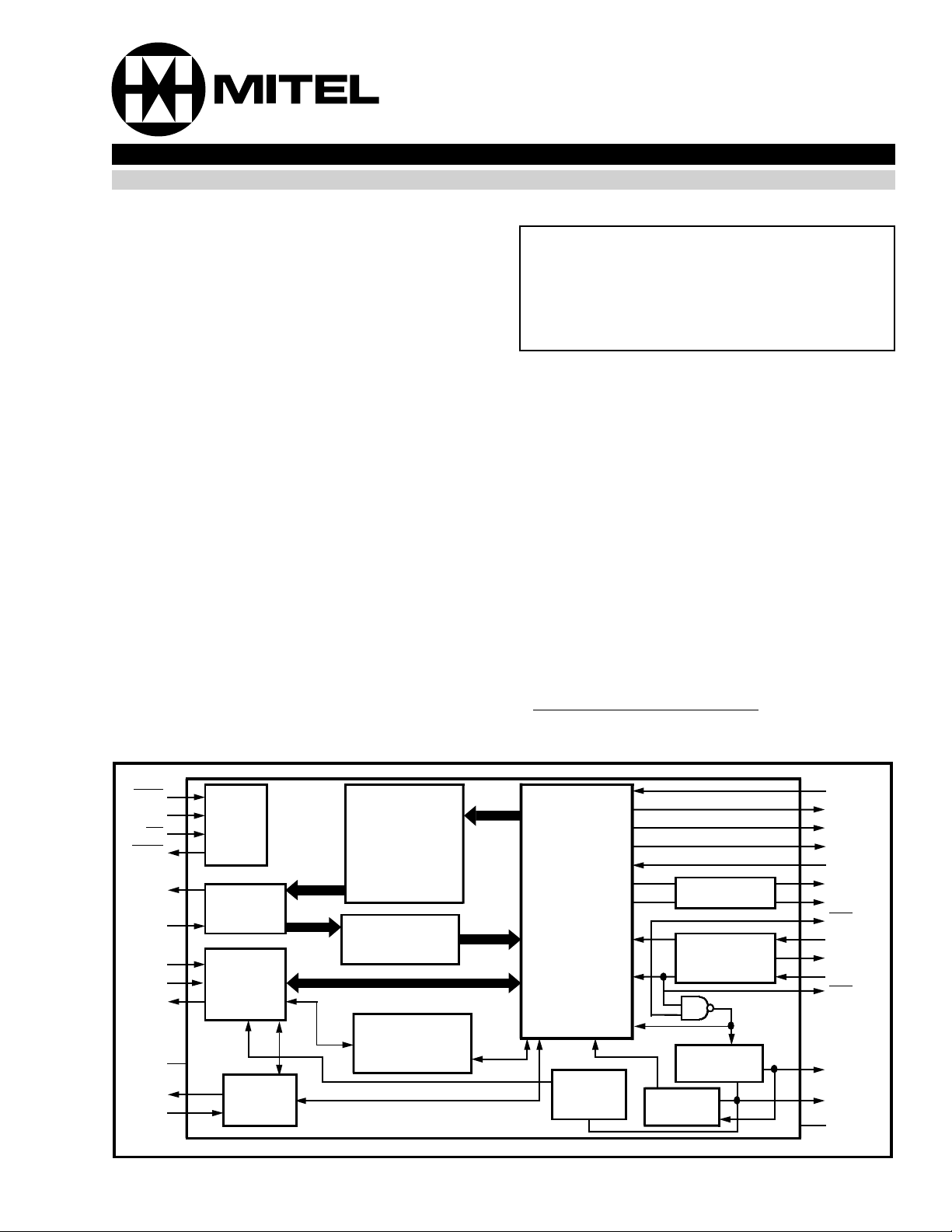
Two Frame
Elastic
Buffer with
Slip Contro l
DS1
LINK
INTERFACE
2048 - 1544
Converte r
ABCD
Signalling RAM
Phase
Detector
Figure 1 - Functional Block Diagram
DS1
Counter
Transmit ter
Receiver
Clock
Extractor
C1.5i
RxFDLClk
RxFDL
TxFDLClk
TxFDL
OUTA
OUTB
RxA
RxT
LOS
RxR
RxB
E1.5o
E8Ko
VSS
4-125
Page 2
MH89770 Preliminary Information
40
NC
39
38
37
36
35
34
33
32
31
30
29
28
27
26
25
24
23
22
21
NC
LOS
NC
TxFDL
NC
TxFDLClk
VSS
RxFDLClk
DSTo
RxFDL
OUTB
C1.5i
RxSF
TxSF
OUTA
NC
NC
NC
VSS
Pin Description
2
NC
NC
XSt
NC
C2i
F0i
3
4
5
6
7
8
9
10
11
12
13
14
15
16
17
18
19
20
E1.5o
VDD
RxA
RxT
RxR
RxB
CSTi1
CSTi0
E8Ko
XCtl
CSTo
DSTi
E1.5o
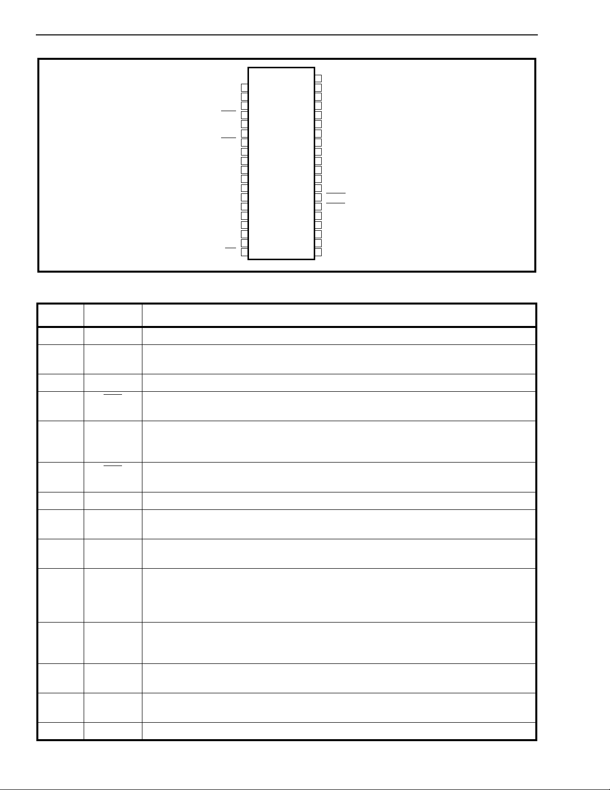
Figure 2 - Pin Connections
Pin # Name Description
2NCNo Connection.
3E1.5o1.544 MHz Extracted Cl ock (Output): Thi s clock is extra cted by the device from the
received DS1 signal. It is used internally to clock in data received at RxT and RxR.
4V
DD
5RxA
System Power Supply. +5V.
Received A (Output): The bipolar DS1 signal received by the device at RxR and RxT is
converted to a unipolar format and output at this pin.
6
7
RxT
RxR
Receive Tip and Ring Inputs: Bipolar split phase inputs designed to be connected
directly to the input transformer. I mpe dance to ground is approximately 1kΩ.
Impedance between pins=430Ω.
8RxB
Received B (Output): The bipolar DS1 signal received by the device at RxR and RxT is
converted to a unipolar format and output at this pin.
9NCNo Connection.
10 CSTi1 Control ST-BUS Input #1: A 2048 kbit/s serial control stream which carries 24
per-channel control words.
11 CSTi0 Control ST-BUS Input #0: A 2048 kbit/s serial control stream that contain s 24 per
channel control words and two master control words.
12 E8Ko 8 kHz Extracted Clock (Output): This is an 8 kHz output generated by dividing the
extracted 1.544 MHz clock by 193 and aligning it with the received DS1 frame. The 8
kHz signal can be used for synchronizing system clocks to the extracted 1.544 MHz
clock. When digital loopback is enabled, the 8kHz is derived from C1.5.
13 XCtl External Control (O utpu t ): This is an uncommitt ed external outpu t pin which is set or
reset via bit 3 in Master Control Word 1 on CSTi0. The state of XCtl is updated once per
frame.
14 XSt External Status (Sch mitt Trigger Input ): The state of this pin is sampled once per
frame and the status is reporte d in bit 5 of Master Status Word 2 on CSTo.
15 CSTo Control ST-BUS Output: This is a 2048 kbit/s serial control stream which provides the
24 per-channel status words, and two master statu s words.
16 NC No Con nec tion .
4-126
Page 3

Preliminary Information MH89770
Pin Description (Continued)
Pin # Name Description
17 DSTi Data ST-BUS Input: This pin accepts a 2048 kbit/s serial stream which contains the 24
PCM or data channels to be transmit ted on the T1 trunk.
18 C2i 2.0 48 MHz Sy stem Clock (Inp ut ): This is the master clo c k for the ST-BUS section of
the chip. All data on the ST-BUS is clocked in on the falling edge of C2i and out on the
rising edge.
19 E1.5o 1.544 MHz Ex tracted Cl ock (Ou tput): Internal ly connected to Pin 3.
20 F0i
Frame Pulse Input: This is the frame synchronizati on signal which def ines the
beginning of the 32 channel ST-BUS frame.
21 V
SS
System ground.
22-24 NC No Con nec tion .
25 OUTA Output A (Open Collector Output): This is the output of the DS1 transmitter circuit. It is
suitable for use with an external pulse transformer to generate the transm it bipolar line
signal.
26 TxSF
Transmit Superfram e Pulse Inp ut: A low pulse applied at this pin will determ ine the
start of the next transmit superframe as illustrated in Figure 20. The device will free run if
this pin is held high.
27 RxSF
Received Superframe Pulse Output: A pulse output on this pin indicates that the next
frame of data on the ST-BUS is from frame 1 of the received superframe. The period is
12 frames long in D3/D4 modes and 24 frames in ESF mode. Active only when device is
synchronized to received DS1 signal.
28 C1.5i 1.544 MHz Clock Inpu t: The rising edge of this clock is used to output data on OUTA,
OUTB. C1.5i must be pha se -lo c ked to the C2i system cl o c k.
29 OUTB Output B (Open Collector Output): This is the output of the DS1 transmitter circuit. It is
suitable for use with an external pulse transformer to generate the transm it bipolar line
signal.
30 RxFDL Received Facility Data Link (Output): A 4 kbit/s serial output stream that is
demultiple xed from the FDL bits in ESF mode, or the received F
bit pattern when in
S
SLC96 mode. It is clocked out on the rising edge of RxFDLClk.
31 DSTo Data ST-BUS Output: A 2048 kbit/s serial output stream which contains the 24 PCM or
data channels received from the DS1 line.
32 RxFDLClk Receive Facility Data Link Cl ock Ou tput: A 4 kHz clock used to output FDL
information on RxF DL. Data is clocked out on the rising edge of the clock.
33 V
SS
No Connection.
34 TxFDLCl k Transmit Facility Data Link Clock Outp ut: A 4 kHz clock used to input FDL
information on TxFDL. Data is cloc ked in on the rising edge of the clock.
35 NC No Con nec tion .
36 TxFDL Transmit Facility Data Link (Input)
FDL bits in the ESF mode, or the F
: A 4 kbit/s serial input stream that is muxed into the
pattern when in SLC96 mode. It is clocked in on the
S
rising edge of TxFDLClk.
37 NC No Con nec tion .
38 LOS Loss of Signal (Output): This pin goes high when 128 contiguous ZEROs are received
on the RxT and RxR inputs. When LOS is high, RxA
and RxB are forced high. LOS is
reset when 48 ones are received in a two T1-frame period.
39 NC No Con nec tion .
40 NC No Connection.
4-127
Page 4
MH89770 Preliminary Information
X
31
MC
W2
31
31
MS
W2
29 30 31
25 26 27 28
21 22 23 24
17 18 19 20
13 14 15 16
9 101112
X
X
X
X
X
X
1
30
PC
CW
1
29
28
26
25
24
22
21
20
18
17
16
14
13
12
10
9
8
15
PC
PC
27
PC
PC
PC
23
PC
PC
PC
19
PC
PC
PC
PC
PC
PC
11
PC
PC
PC
7
CW
CW
X
CW
CW
CW
X
CW
CW
CW
X
CW
CW
CW
MC
CW
CW
CW
X
CW
CW
CW
X
1
1
1
1
1
1
1
1
1
1
W1
1
1
1
1
1
1
29 30 31
X
25 26 27 28
X
21 22 23 24
X
17 18 19 20
X
13 14 15 16
X
9101112
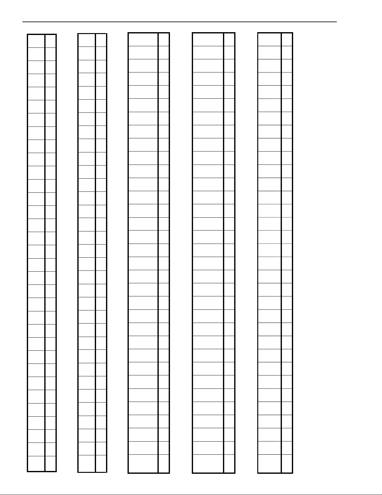
ST-BUS CHANNE L VERSUS DS1 CHANNEL TRANSMITTED
X
ST-BUS CHANNEL V ERSUS DS1 CHANNEL RECEIVED
30
29
28
26
25
24
22
21
20
18
17
16
14
13
12
10
9
ST-BUS CHANNEL VERSUS DS1 CHANNEL CONTROLLED
8
PC
PC
PC
27
PC
PC
PC
23
PC
PC
PC
19
PC
PC
PC
15
PC
PC
PC
11
PC
PC
PC
7
CW
CW
CW
X
CW
CW
CW
X
CW
CW
CW
X
CW
CW
CW
X
CW
CW
CW
X
CW
CW
CW
X
2
2
2
2
2
2
2
2
2
2
2
2
2
2
2
2
2
2
ST-BUS CHANNEL VERSUS DS1 CHANNEL CONTROLLED
15
30
29
28
26
25
24
22
21
20
18
17
16
14
13
12
10
9
8
27
23
19
MS
11
7
PCS
PCS
PCS
X
PCS
PCS
PCS
X
PCS
PCS
PCS
X
PCS
PCS
PCS
W1
PCS
PCS
PCS
X
PCS
PCS
PCS
X
W
W
W
W
W
W
W
W
W
W
W
W
W
W
W
Figure 3 - ST-BUS Channel Allocations
W
W
W
ST-BUS VERSUS DS1 CHANNEL STATUS
5678
X
1234
X
DSTi 0
DS1 1 2 3 4 5 6 7 8 9 10 11 12 13 14 15 16 17 18 19 20 21 22 23 24
4-128
5678
X
1234
X
DSTo 0
DS1 1 2 3 4 5 6 7 8 9 10 11 12 13 14 15 16 17 18 19 20 21 22 23 24
6
1
PC
CW
5
1
PC
CW
4
1
PC
CW
3
X
2
1
PC
CW
1
1
PC
CW
1
PC
CW
CSTi0 0
DS1 1 2 3 4 5 6 7 8 9 10 11 12 13 14 15 16 17 18 19 20 21 22 23 24
PCCW=Per Channe l C on tr o l Wo r d, MCW1/2=Mas ter Control W o rd 1/2
6
5
4
2
1
0
CSTi1
PC
PC
PC
3
PC
PC
PC
CW
CW
CW
X
CW
CW
CW
2
2
2
2
2
2
DS1 1 2 3 4 5 6 7 8 9 10 11 12 13 14 15 16 17 18 19 20 21 22 23 24
PCCW=Per Channe l C on tr o l Wo r d
6
PCS
5
PCS
4
PCS
3PSW
2
PCS
1
PCS
PCS
CSTo 0
W
W
W
W
W
W
DS1 1 2 3 4 5 6 7 8 9 10 11 12 13 14 15 16 17 18 19 20 21 22 23 24
PCSW=Per Channel Status Word, PSW=Phase Status Word, MSW=Master Status Word
X = UNUSED
Page 5

Preliminary Information MH89770
Functional Description
The MH89770 is a thick film hybrid solution for a T1
interface. All of the formatting and signalling
insertion and detection is done by the device.
Various programmable options in the device include:
ESF, D3/D4 or SLC-96 mode, common channel or
robbed bit signalling, zero code suppression, alarms,
and local and remote loopback. The MH89770 also
has built in bipolar line drivers and receivers and a
clock extraction circuit.
All data and control information is communicated to
the MH89770 via 2048 kbit/s serial streams
conforming to Mitel’s ST-BUS format.
The ST-BUS is a TDM serial bus that operates at
2048 kbits/s. The serial streams are divided into 125
µsec frames that are made up of 32 8-bit channels. A
serial stream that is made up of these 32 8 bit
channels is known as an ST-BUS stream, and one of
these 64 kbit/s channels is known as an ST-BUS
channel.
The system side of the MH89770 is made up of
ST-BUS inputs and outputs, i.e., control inputs and
outputs (CSTi/o) and data inputs and outputs
(DSTi/ o). These signals are functionally represented
in Figure 32. The DS1 line side of the device is made
up of split phase inputs (RxT, RxR) and outputs
(OUTA, OUTB) which can be connected to line
coupling transformers. Functional transmit and
receive timing is shown in Figures 33 and 34.
Data for transmission on the DS1 line is clocked
serially into the device at the DSTi pin. The DSTi pin
accepts a 32 channel time division multiplexed
ST-BUS stream. Data is clocked in with the falling
edge of the C2i clock. ST-BUS frame boundaries are
defined by the frame pulse applied at the F0i
Only 24 of the available 32 c hannels on the ST-BUS
serial stream are actually transmitted on the DS1
side. The unused 8 channels are ignored by the
device.
Data recei ved from the DS1 l ine is clocked out of th e
device in a similar manner at the DSTo pin. Data is
clocked out on the rising edge of the C2i clock. Only
24 of the 32 channels output by the device contain
the information from the DS1 line. The DSTo pin is,
however, actively driven during the unused channel
timeslots. Figure 3 shows the correspondence
between the DS1 channels and the ST-BUS
channels.
All control and monitoring of the device is
accomplished through two ST-BUS serial control
pin.
inputs and one ser ial control outpu t. Control ST-BUS
input number 0 (CSTi0) accepts an ST-BUS serial
stream which contains the 24 per channel control
words and two master control words. The per channel
control words relate directly to the 24 information
channels output on the DS1 side. The master control
words affect operation of the whole device. Control
ST-B US input n umber 1 (CSTi1) accepts an ST-BUS
stream containing the A, B, C and D signalling bits.
The relationship between the CSTi channels and the
controlled DS0 channels is shown in Figure 3. Status
and signalling information is received from the device
via the control ST-BUS output (CSTo). This serial
outpu t stream contain s two m aster st atus wo rds, 24
per channel status words and one Phase Status
Word. Figure 3 shows the correspondence between
the received DS1 channels and the status words.
Detailed information on the operation of the control
interface is presented be low.
Programmable Features
The main features in the device are programmed
through two master control words which occupy
channels 15 and 31 in Control ST-BUS input stream
number 0 (CSTi0). These two eight bit words are
used to:
• Select the di fferent operati ng mo de s of the
device ESF, D3/D4 or SLC-96.
• Activate th e fea tures th at are n ee ded in a
certain application; common channel signalling,
zero code s uppressi on , signal ling d eboun ce,
etc.
• Turn on in service alarm s, d iagno stic lo op
arounds, and the ext erna l cont rol funct ion
Tables 1 and 2 contain a complete explanation of the
function of the different bits in Master Control Words
1 and 2.
Major Operating Modes
The major operating modes of the device are
enabled by bits 2 and 4 of Master Control Word 2.
The Extended Superframe (ESF) mode is enabled
when bit 4 is set high. Bit 2 has no effect in this
mode. The ESF mode enables the t ransmission of
the S bit pattern shown in Table 3. This includes the
frame/superframe pattern, the CRC-6, and the
Facility Data Link (FDL). The device generates the
frame/multiframe pattern and calculates the CRC for
each superframe. The data clocked into the device
on the TxFDL pin is incorporated into the FDL. ESF
mode will also ins e rt A, B, C and D si gnalling bits into
the 24 f rame multiframe. The DS1 frame begins after
4-129
Page 6

MH89770 Preliminary Information
Bit Name Description
7 Debounce When set the received A, B, C and D signalling bits are reported directly in the per
channel status words output at CSTo. When clear, the signalling bits are debounced for 6
to 9 ms before they are placed on CSTo.
6 TSPZCS Transparent Zero Code Suppression. When this bit is set, no zero code suppression is
implemented.
5 B8ZS Binary E ight Zero Suppr essi on . When this bit is set, B8ZS zero code suppression is
enabled. When clea r, bit 7 in data channels containing all zeros is for ced high before
being transmitted on the DS1 side. This bit is inactive if the TSPZ CS bit is set.
4 8kHSel 8 kHz Output Select. Whe n set, the E8Ko pin is held hig h. When clear, the E8Ko
generates an 8 kHz output derived from the extracted 1.544 MH z clock or C1.5i clock
(see Pin Description for E8Ko).
3 XCtl External Control Pin. When set, the XCtl pin is held high. Whe n clear, XCtl is held low.
2 ESFYLW ESF Yellow Alarm. Valid only in ESF mode. When set, a sequence of eight 1’s followed
by eight 0’s is sent in the FDL bit positions. When clear , the FDL bit contains data input at
the TxFDL pin.
1 Robbed bit When this bit is set, robbed bit signalling is disabled on all DS0 transmit channels. When
clear, A, B, C and D signalling bits are inserted into bit position 8 of all DS0 channels in
every 6th frame.
0 YLALR Yellow Alarm. When set, bit 2 of all DS0 channels is set low. When clear, bit 2 operates
normally.
Table 1. Master Control Word 1 (Channel 15, CSTi0)
.
Bit Na me Description
7 RMLOOP Remote Loopback. When set, the data received at RxR and RxT is looped back to OUTB
and OUTA respectively. The data is clocked into the device with the extracted 1.544 MHz
clock. The device still monit ors the received dat a and outpu ts it at DSTo. The device
operates normally when the bit is clear.
6 DGLOOP Digital Loop back . When set, the data input on DSTi is looped around to DSTo. The
normal received data on RxR and RxT is ignored. However, t he dat a input at DSTi is still
transmitted on OUTA and OUTB. The device frames up on the looped data using the C1.5i
clock.
5 ALL1'S All One’s Alarm. When set, the chip tra nsmit s an unfram ed all 1's signal on OUTA and
OUTB.
4 ESF/D4 ESF/D4 Select. When set, the device is in ESF mode. When clear, the device is in D3/D4
mode.
3 ReFR Reframe. If set for at least one frame and then cleared, the chip will begi n to sea rch for a
new frame position. Only th e change from high to low will cause a reframe, not a
continuous low level.
2 S LC -96 SLC-96 Mode Select. The chip is in SLC-96 mode when this bit is set. This enables input
and output of the F
bit pattern using the same pins as the facilit y data link in ESF mode .
S
The chip will use the same framing algorithm as D3/D4 mod e. The user must insert the
valid F
bits in 2 out of 6 superframes to allow the receiver to find superframe sync, and
S
the transmitter to insert A and B bits in every 6th frame. The SLC-96 FDL completely
replaces the F
pattern in the outgoing S bit positi on. Inacti ve in ES F mode.
S
1 CRC/MIM IC In ESF mode, when set, the chip disregards the CRC calculat ion durin g synchronization .
When clear, the device will check for a correct CRC before going into synchronization. In
D3/D4 mode, when set, the device will synchronize on the first correct S-bit pattern
detected. When this bit is clear , the device will not synchronize if it has detected more than
one candidate for the frame alignm ent pat te rn (i.e., a mimic ).
0 Maint. M ain tenan ce Mode . When set, the device will declare itself out-of-sync if 4 out of 12
consecutive F
bits. In this mode, four consecutive bits following an errored F
bits are in error. When clear, the out-of-sync threshold is 2 errors in 4 FT
T
bit are examined.
T
Table 2. Master Control Word 2 (Channel 31, CSTi0)
4-130
Page 7

Preliminary Information MH89770
approximately 25 periods of the C1.5i clock from the
F0i
frame pulse.
Frame # F PS FDL CRC Signalling
†
1X
2CB1
3X
40
5X
6CB2A
7X
80
9X
10 CB3
11 X
12 1 B
13 X
14 CB4
15 X
16 0
17 X
18 CB5 C
19 X
20 1
21 X
22 CB6
23 X
24 1 D
Table 3. ESF Fra me Pat ter n
† These signalling bits are only valid if the robbed bit signal ling is
active.
‡
During synchronization the receiver locks on to the
incoming frame, calculates the CRC and compares it
to the CRC received in the next multiframe. The
device will not declare itself to be in synchronization unless a valid framing pattern in the S-bit is
detected and a correct CRC is received. The CRC
check in this case provides protection against false
framing. The CRC check can be turned off by setting
bit 1 in Master Control Word 2.
The device can be forced to resynchronize itself. If
Bit 3 in Master Cont rol Word 2 is set for one frame
and then subsequently reset, the de vice will start to
search for a new frame position. The decision to
reframe is made by the user’s system processor on
the basis of the status conditions detected in the
received master status words. This may include
consideration of the number of errors in the received
CRC in conjunction with an indication of the
presence of a mimic. When the device attains
synchronization the mimic bit in M aster Status Word
1 is set if the device found another possible
candidate when it was searching for the framing
pattern.
FPS) exceed the threshold set with bit 0 in Master
Control Wor d 2.
Frame # F
T
F
S
Signalling
†
11
20
30
40
51
61A
70
81
91
10 1
11 0
12 0 B
Table 4. D3/D4 Framer
† These signalling bits are only valid if the robbed bit signalling is
active.
Standard D3/D4 framing is enabled when bit 4 of
Master Control Word 2 is reset (logic 0). In this mode
the device searches for and inserts the framing
pattern shown in Table 4. This mode only supports
AB bit signalling, and does not contain a CRC check.
The CRC/MIMIC bit in Master Control Word 2, when
set high, allows the device to synchronize in the
presence of a mimic. If this bit is reset, the device will
not synchronize in the presence of a mimic. (Also
refer t o section on Framing Algorithm.)
In the D3/D4 mode the device can also be made
compatible with SLC-96 by setting bit two of Master
Control Word 2. This allows the user to insert and
extract the signalling framing pattern on the DS1 bit
stream using the FDL input and output pins. The
user must format this 4 kbits of information externally
to meet all of the requirements of the SLC-96
specification (see Table 5). The device multiplexes
and demultiplexes this information into the proper
position. This mode of operat ion can also be used for
any other application that uses all or part of the
signalling framing pattern. As long as the serial
stream clocked into the TxFDL contains two proper
sets of consecutive synchronization bits (as shown in
Table 5 for fr am es 1 to 2 4) , the device will be
able to insert and extract the A, B signalling bits.
The TxSF
pin should be held high in this mode.
Superframe boundaries cannot be defined by a pulse
on this inp ut. The RxSF
output functions normally
and indicates the superframe boundaries based on
the synchronization pattern in the F
received bit
S
position.
Note that the devi ce wi ll resync hroniz e auto mati cally
if the errors in the terminal framing pattern (F
T
or
4-131
Page 8
MH89770 Preliminary Information
Frame
#
F
T
11
†
F
S
Notes
Frame
#
37 1
F
T
†
F
S
20 38X
30 390
40 40X
51 411
60 42X
70 430
81 44X
91 451
10 1 46 X
11 0 47 0
12 1 48 S
13 1 49 1
14 0 50 S
Resynchronization
Data
Bits
15 0 51 0
16 0 52 S
17 1 53 1
18 0 54 C
19 0 55 0
20 1 56 C
21 1 57 1
22 1 58 C
23 0 59 0
24 1 60 A
25 1
61 1
26 X 62 A
27 0 63 0
28 X 64 L
29 1 65 1
30 X 66 L
31 0 67 0
X =Concentrator
Fiel d Bi ts
32 X 68 L
33 1 69 1
34 X 70 L
35 0 71 0
36 X 72 S
Tab le 5. S LC-96 Fram ing P attern
† Note: The FS pattern has to be supplied by the user.
Notes
X = Concentrator
Field B i ts
S = Spoiler Bits
C = Maintenance
Field
Bits
A = Alarm Field
Bits
L = Line S wi tc h
Field B i ts
S = Spoiler Bits
4-132
DATA
B8ZS
B8ZS
B0 00V
B
000
B
V
B
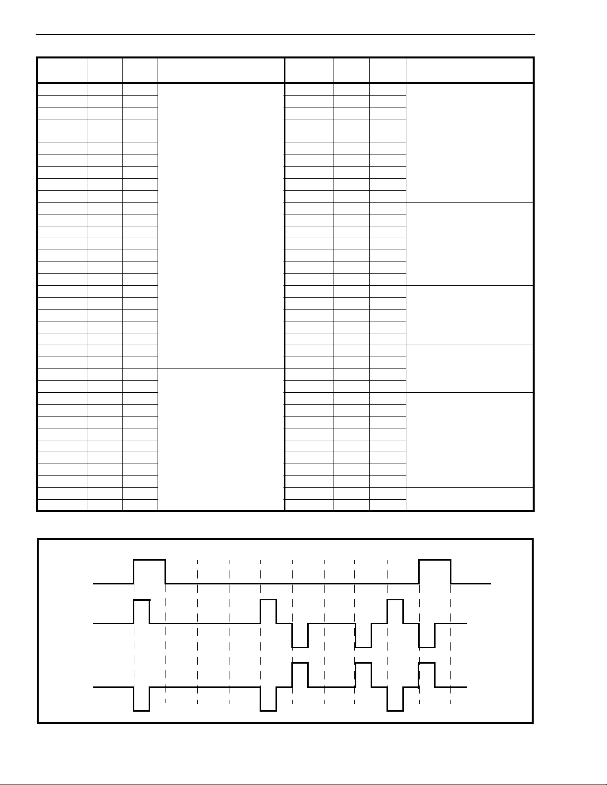
Figure 4 - B8ZS Output Coding
0
V
V
0
B
B
B
B
V = Violation
B = Bipolar
0 = No Pulse
Page 9

Preliminary Information MH89770
Zero Code Suppression
The combination of bits 5 and 6 in Master Control
Word 1 allow one of three zero code suppression
schemes to be selected. The three choices are:
none, binary 8 zero suppression (B8ZS), or jammed
bit (bit 7 forced high). No zero code suppression
allows the device to interface with systems that have
already applied some form of zero code suppression
to the data input on DSTi. B8ZS zero code
suppression replaces all strings of 8 zeros with a
known bit pattern and a specific pattern of bipolar
violations. This bit pattern and violation pattern is
shown in Figure 4. The receiver monitors the
received bit pattern and the bipolar violation pattern
and replaces all matching strings wit h 8 zeros.
Loopback Modes
Remote and digital loopback modes are enabled by
bits 6 and 7 in Master Cont rol Word 2. These modes
can be used for diagnostics in locating the source of
a fault condition. Remote loop around loops back
data received at RxR and RxT back out on OUTA
and OUTB, thus effectively sending the received
DS1 data back to the far end unaltered so that the
transmission line can be tested. The received signal
with the appropriate received channels on the DS1
side made available in the proper format at DSTo.
The digital loop around mode diverts the data
received at DSTi back out the DSTo pin. Data
received on DSTi is, however, still t ransmitted out via
OUTA and OUTB. This loop back mode can be used
to test the near end interface equipment when there
is no transmission line or when there is a suspected
fail ure of th e line .
The all ones transmit alarm (also known as the blue
alarm or the keep alive signal) can be activated in
conjunction with the digital loop around so that the
transmission line sends an all 1's signal while the
normal data is looped back locally.
The MH89770 also has a per channel loopback
mode. See Table 6 and the following section for more
information.
Per Channel Control Feature s
In addition to the two master control words in CSTi0
there are also 24 Per Channel Control Words. These
control words only affect individual DS0 channels.
The correspondence between the channels on
CSTi0 and the affected DS0 channel is shown in
Fig. 3. Each control word has three bits that enable
robbed bit signalling, DS0 channel loopback and
inversion of the DS0 channel. A full description of
each of the bits is provided in Table 6.
Transmit Signalling Bits
Control ST-BUS input number 1 (CSTi1) contains 24
additional per channel control words. These 24
ST-BUS channels contain the A, B, C and D
signalling bits that the device uses at transmit time.
The position of these 24 per channel control words in
the ST-BUS is
the ABCD signalling bits is shown in Table 7. Even
though the device only inserts the signalling
shown in Figure 3 and the position of
Bit Name Description
7-3 IC Internal Connections. Must be kept at 0 for normal operation.
2 Polarity When set, the applicable channel is not inverted on the transmit or the receive side of
the device. When clear, all the bits within the applicable channel are inverted both on
transmit and receive side.
1 Loop Per C ha nne l Loop back. When set, the received DS0 channel is replaced with the
transmitted DS0 channel. Only one DS0 channel may be looped back in this manner at
a time. The transmitted DS0 channel remains unaffected. When cl ear the transmi t and
receive DS0 sections operate normally.
0 Data Data Channel Enable. When set, robbed bit signalli ng for th e applicabl e channel is
disabled. When clear, every 6th DS1 frame is available for robbed bit signalling. This
feature is enabled only if bit 1 in Master Control Word is low.
Table 6. Per Channel Control Word 1 Input at CSTi0
Bit Name Descri ptio n
7-4 Unuse d Keep at 0 for normal operation
3
2
1-0
A
B
C, D
These are the 4 signalling bits inserted in the appropriate channels of the DS1 stream
being output from the chip, when in ESF mode. In D3/D4 modes where there are only
two signalling bits, the values of C and D are ignored.
Table 7. Per Channel Control Word 2 Input at CSTi1
4-133
Page 10

MH89770 Preliminary Information
Bit Name Description
7 YL ALR Yellow Alarm In dicatio n. This bit is set when the chip is receiving a 0 in bit position 2
of every DS0 channel.
6MIMICThis bit is set if the frame search algorithm found more than one possible frame
candidate when it went into frame synchronization.
5 ERR Term i na l Fram ing Bit Error. The state of this bit changes every time the chip detects
4 errors in the F
96ms.
4 ESF YLW ESF Yellow Alarm. This bit is set when the device has observed a sequence of eight
one’s and eight 0’s in the FDL bit positions.
3MFSYNC
Multiframe Synchronization. This bit is cleared when D3/D4 multifram e
synchronization has been achieved. Applicable only in D3/D4 and SLC-96 modes of
operation.
2 BPV Bipolar Violation Count. The state of this bit changes every time the device counts
256 bipolar violations.
1 SLIP Slip In di cation. This bit changes state every time the elastic buffer in the device
performs a controlled slip.
0 SYN
Synchronizatio n. This bit is set when the device has not achieved synchronizat ion.
The bit is clear when the device has synchronized to the received DS1 data stream.
Tab le 8 . Master Statu s Word 1 (Chan nel 15 , CSTo)
or FPS bit pattern. The bit will not change state more than once every
T
.
Bit Name Description
7 BlAlm Bl ue Al arm . This bit is set if the receiver has detected two frames of 1’s and an out of
frame condition. It is reset by any 250 microsecond interval that contain s a zero.
6 FrCn t Frame Count. This is the ninth and most signifi cant bit of the “Phase Stat us Word”
(see Table 10). If the phase status word is increment ing, this bit will toggle when th e
phase reading ex ceeds channel 31, bit 7. If the phase word is decrementing, then this
bit will toggle when the reading goes below channel 0, bit 0.
5 XSt External Status. This bit reflects the state of the external status pin (XSt). The state of
the XSt pin is sampled once per frame.
4-3 BPVCnt Bipolar Violation Count. These two bits change state every 128 and every 64 bipolar
violations, respectively.
2-0 CRCCNT CRC Error Count. These three bits count received CRC errors. The counter will reset
to zero when it reaches terminal count. Valid only in ESF mode.
Tab le 9 . Master Statu s Word 2 (Chan nel 31 , CSTo)
Bit Name Descri ptio n
7-3 ChannelCnt Channel Count. These five bits indicate the ST-BUS channel count between the
ST-BUS frame pulse and the rising edge of E8Ko.
2-0 BitCnt Bit Cou nt. These three bits provide one bit resolutio n within the channel count
described above.
Table 10. Phase Status Word (Channel 3, CSTo)
information in every 6th DS1 frame this information
Operating Status Information
must be input every S T-BUS frame.
Status Information regarding the operation of the
Robbed bit signalling can be disabled for all
channels on the DS1 link by bit 1 of Master Control
Word 1. It can also be disabled on a per channel
basis by bit 0 in the Per Channel Control Word 1.
device is output serially via the Control ST-BUS
output (CSTo). The CSTo serial stream contains
Master Status Words 1 and 2, 24 Per Channel Status
Words, and a Pha se Status Word . The Ma ster Statu s
Words contain all of the information needed to
determine the state of the interface and how well it is
operating. The information provided includes frame
and super frame synchronization, slip, bipolar
4-134
Page 11

Preliminary Information MH89770
Bit Name Description
7-4 Unused Unused Bits. Will be output as 0’s.
3
2
1
0
A
B
C
These are the 4 signalling bits as extracted from the received DS1 bit stream.
The bits are debounced for 6 to 9 ms if the debounce feature is enabled via bit 7 in
Master Control Word 1.
D
Table 11. Per Channel Status Word Output on CSTo
.
violation counter, alarms, CRC error count, FT error
count, synchronization pattern mimic and a phase
status word. Tables 8 and 9 give a description of each
of the bits in Master Status Words 1 and 2, and Table
10 gives a des crip t ion of the Phase Status Wor d.
In addition, the MH89770 has a Loss of Signal (LOS)
pin that is set High when 128 conse cutive ZER O s are
received. While LOS is set High, RxA
and RxB are
forced High. The LOS signal goes Low when a ONEs
density on 12.5% of the bits (equivalent to 48 bits)
occurs in a two DS1 frame period.
Alarm Detect ion
The device detects the yellow alarm for both D3/D4
frame format and ESF format. The D3/D4 yellow
alarm will be activated if a ‘0’ is received in bit
position 2 of every DS0 channel for 600 msec. It will
be released in 200 msec after t he content s of the bit
change. The alarm is detectable in the presence of
errors on the line. The ESF yellow alarm will become
active when the device has detected a string of eight
0’s followed b y eight 1’s i n the facili ty data link. It is
not detectable in the presence of errors on the line.
This means that the ESF yellow alarm will drop out
for rela tive ly short p er iod s o f time, s o t he s y stem will
have to integrate the ESF yellow alarm. The blue
alarm signal, in Master Status Word 2, will also drop
out if there are errors on the line.
Mimic Detection
The mimic bit in Ma ster Status Word 1 w ill be set if,
during synchronization, a frame alignment pattern
(F
or FPS bit pattern) was observed in more than
T
one position, i.e., if more than one candidate for the
frame synchronization position was observed. It will
be reset when the de v i ce resynchroniz e s. The mimic
bit, the terminal framing error bit and the CRC error
counter can be used separately or together to decide
if the rec eiv e r s ho u ld b e fo r c ed to r e fra me.
Bipolar Violation Counter
The Bipolar Violation bit in Master Status Word 1 will
toggle after 256 violations have been detected in the
received signal. It has a maximum refresh time of 96
ms. This means that the bit can not change state
faster than once every 96 ms. For example, if there
are 256 violations in 80 ms the BPV bit will not
change state until 96 ms. Any more errors in that
extra 16 ms are not counted. If there are 256 errors
in 200 ms then the BPV bit will change state after
200 ms. In practical terms this puts an upper limit
on the error rate that can be calculated from the BPV
information, but this rate (1.7 X 10
-3
) is well above
any normal operating condition.
Bits 4 and 3 also provide bipolar violations
infor-mation. Bit 4 will change state after 128
violations. Bit 3 changes state after 64 bipolar
violations. These bits are refreshed independently
and are not subject to the 96 ms refresh rate
described above.
DS1/ST-BUS Phase Difference
An indication of the phase difference between the
ST-BUS and the DS1 frame can be ascertained from
the information provided by the eight bit Phase
Status Word and the F rame Count bit. Channel t hree
on CSTo contains the Phase Status Word. Bits 7-3 in
this word indicate the number of ST-BUS channels
between the ST-BUS frame pulse and the rising
edge of the E8Ko signal. The remaining three bits
provide one bit resolution within the channel count
indicated by bits 7-3. The fr ame count bit in Master
Status Word 2 is the ninth and most significant bit of
the phase status word. It will toggle when the phase
status word increments above channel 31, bit 7 or
decrements below channel 0, bit 0. The E8Ko signal
has a specific relationship with received DS1 frame.
The rising edge of E8Ko occurs during bit 2, channel
17 of the received DS1 frame. The Phase Status
Word in conjunction with the frame count bit, can be
used to monitor the phase relationship between the
received DS1 frame and the local ST-BUS frame.
The local 2.048 MHz ST-BUS clock must be
phase-locked to the 1.544 MHz clock extracted from
the received data. When the two clocks are not
phase-locked, the input data rate on the DS1 side
will differ from the output data rate on the ST-BUS
side. If the average input data rat e is higher than the
4-135
Page 12
MH89770 Preliminary Information
average output data rate, the channel count and bit
count in the phase status word will be seen to
decrease over time, indicating that the E8Ko rising
edge, and therefore the DS1 frame boundary is
moving with respect to the ST-BUS frame pulse.
Conversely, a lower average input data rate will
result in an increase in the phase reading.
In an application where it is necessary to minimize
jitter transfer from the received clock to the local
system clock, a phase lock loop with a relatively
large time constant can be implemented using
information provided by the phase status word. In
such a system, the local 2.048 MHz clock is derived
from a precision VCO. Frequency corrections are
made on the basis of the average trend observed in
the phase status word. For ex am ple, if the channel
count in the phase status word is seen to increase
over time, the feedback applied to the VCO is used
to decrease the system clock frequency until a
reversal in the trend is observed.
The elastic buffer in the MT8977 permits the device
to handle 26 ST-BUS channels or 156 UI of jitter/
wander (see description of elastic buff er in the next
section). In order to prevent slips from occurring, the
frequency corrections would have to be implemented
such that the deviation in the phase status word is
limited to 26 channels peak-to-peak. It is possible to
use a more sophisticated protocol, which would
center the elastic buffer and permit more
jitter/wander to be handled. However, for most
applications, including ACCUNE T
®
T1.5 (138 UI), the
156 UI of jitt er/wander tolerance is acceptable.
Received Signalling Bits
a random transition stage until the device attains
multiframe synchronization.
Clock and Framing Signals
The MH89770 has a built in clock extraction circuit
which creates a 1.544 MHz clock synchronized to
the received DS1 signal. This c lock is used internally
by the MH89770 to clock in data received on RxT
and RxR, and is also output at the E1.5o pin. The
circuit has been designed to operate within the
constraints imposed by the minimum 1’s density
requirements, typically specified for T1 networks
(maximum of 15 consecutive 0’s).
The extracted clock is internally divided by 193 and
aligned with the received DS1 frame. The resulting 8
kHz signal is outpu t at the E8Ko pin and can be used
to phase lock the local system C2 and the transm it
C1.5 clo cks to the extracted clock.
The MH89770 requires three clock signals which
have to be generated externally. The ST-BUS
interface on the device requires a 2.048 MHz signal
which is applied at the C2i pin and an 8 kHz
framing signal applied at the F0i
signal is used to delimit individual ST-BUS frames.
Figure 19 illustrates the relationship between the C2i
and F0i
signals. The F0i signal can be derived from
the 2.048 MHz C2 clock. The transmit side of the
DS1 interface requires a 1.544 MHz clock applied at
C1.5i. The C1.5 and C2 clocks must be phase
locked. There must be 193 clock cycles of the C1.5
clock for every 256 cycles of the C2 clock in order for
the 2.048 to 1.544 rate converter to function properly.
pin. The framing
The A, B, C and D signalling bits are output from the
device in the 24 Per Channel Status Words. Their
location in the serial steam output at CSTo is shown
in Figure 3 and the bit positions are shown in Table
11. The internal debouncing of the signalling bits can
be turned on or off by Master Control Word 1. In ESF
mode, A, B, C and D bits are valid. Even though the
signalling bits are only received once every six
frames the device stores the information so that it is
available on the ST-BUS every frame. The ST-BUS
will always contain the most recent signalling bits.
The state of the signalling bits is frozen if
synchronization is lost.
In D3/D4 mode, only the A and B bits are valid. The
state of the signalling bits is frozen when terminal
frame synchronization is lost. The freeze is disabled
when the device regains terminal frame
synchronization. The signalling bits may go through
4-136
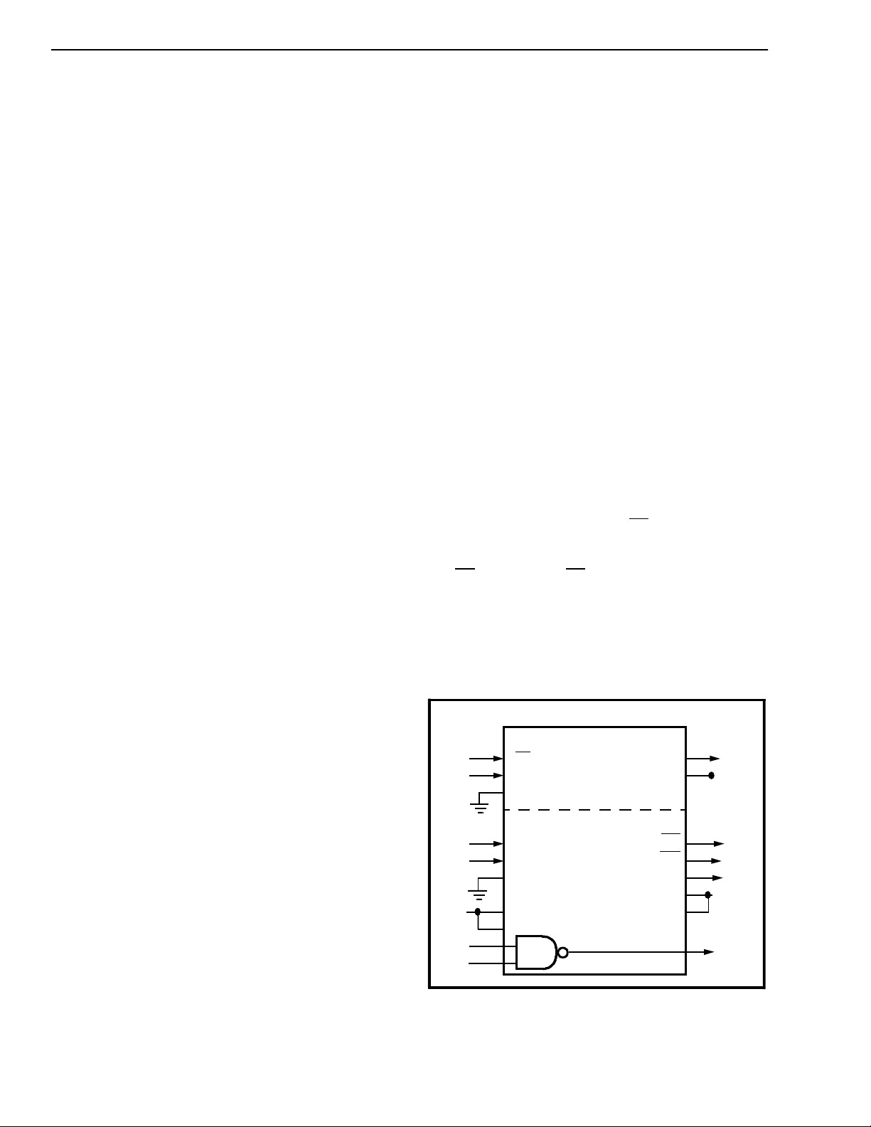
MT8941
DPLL #1
F0i
C12i
MS1
DPLL #2
C8Kb
C16i
MS0
ENC4o
5V
Ai
Bi
MS2
MS3
ENC2o
Figure 5 - MT8941 Clock Generator
CVb
ENCv
F0b
C4b
C2o
C1.5
+5V
F0i
C4i
C2i
+5V
Yo
Page 13
Preliminary Information MH89770
MH89770
Transmit
Data
OUTA
+12V
OUTB
E1.5o
RxA
RxB
RxT
C2
L2
TR1
1:
:0.5
1:
TR2
R1
L1
C1
S1
S2
S3
S4
S5
S6
S7
MH89761
EIT
EIR
EA
EB
EC
SW
RCLT
RCHT
RCLR
RCHR
Ti
Ri
TxT
TxR
TL
RL
Rx
Extracted
Clock
Received
Data
COMPONENT VALUES:
R1 = 150Ω 1% W
C1 = 0.01 µF 5% 250V
C2 = 0.47 µF 5% 100V
L1 = 33 µH 130mA
L2 = 33 µH 165 mA
TR1 = 1:1:0.5 Filtran* Part # TFS2573
TR2 = 1:1:1 Filtran* Part # TFS25 74
*Filtran Ltd .
229 Colonnade Road
Nepean, Ontario
Canada K2E 7K3
613-226-1626
Line
Receiver
1
4
+5V
RxR
V
DD
1:
:1
1:
0-150’
S1
S2
S4
S4
S5
S6
S7
Note: The equalizer has been optimized for 22 gauge ABAM
cable. The exact distances may vary with the type of cable and the
output trans former. Different line length settings may be
require d if a tran sform e r other tha n the Filtra n TFS 2573 is used .
CLOSE
OPEN
OPEN
OPEN
OPEN
OPEN
OPEN
Equalizer setting s
150-450’
OPEN
CLOSE
OPEN
CLOSE
OPEN
CLOSE
OPEN
450-655’
OPEN
OPEN
CLOSE
OPEN
CLOSE
OPEN
CLOSE
Figure 6 - Input/Output Configuration
4-137
Page 14
MH89770 Preliminary Information
In synchronous operation the slave end of the link
must have its C2 and C1.5 clocks phase locked to
the extracted clock. In plesiochronous clocking
applications where the master and slave end are
operating under controlled slip conditions, phase
locking to the extracted clock is generally not
required.
Mitel’s MT8941 Digital Phase Lock Loop (DPLL) can
be used to generat e all timing signals required by the
MH89770. The MT8941 has two DPLLs built into the
device. Figure 5 shows how DPLL #1 can be set up
to generate the C1.5 clock phase locked to the F0i
which in turn is derived from the same source as the
C2 clock. Figure 5 also shows how DPLL #2 is set up
to generate the ST-BUS clocks that are phas e locked
to the received da ta ra te . If E8Ko from th e MH89770
is connected to the C8Kb input on the MT8941,
DPLL #2 in the device will generate the ST-BUS
clocks that are phase locked to the T1 line.
DS1 Line Int erface
Line Transmitter
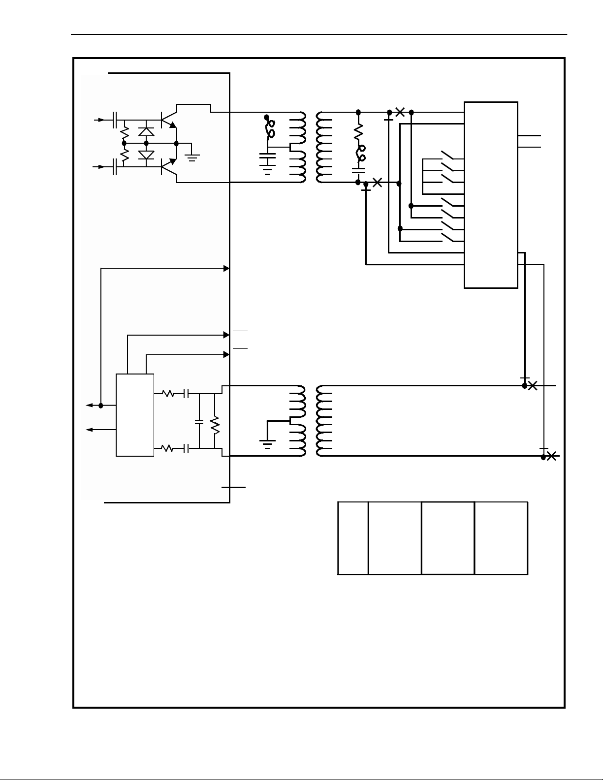
The transmit line interface is made up of two open
collector drivers (OUTA and OUTB) that can be
coupled to the line with a center tapped pulse
transformer (see Figure 6). A step function is applied
to the transformer when either of the transistors is
turned on. By operating in the transient portion of the
inductance response, the secondary of the
transformer produces an almost square pulse. The
capacitor and inductor on the center tap of the
transmit transformer shown in Figure 6 suppress
transients in the 12 volt supply. The series RLC
across the output of the t ransformer shape the pulse
to meet the AT & T or CCITT pulse templates. A
detailed transformer specification is presented in the
applications section of this data sheet.
To complete the interfaces to the transmit line, a
pre-equalizer and line impedance matching network
is required. The pulse output at the transformer
secondary must be pre-equalized to drive different
lengths of cable. Mitel‘s MH89761 T1 Equalizer is
configurable to provide pre-emphasis for 0-150,
150-450 and 450-655 foot lengths of 22 AWG
transmission line. A separate 6dB pad is also
provided on the MH89761 for use in implementing
external looparound. Both circuits have input and
output impedance of 100Ω. Figure 6 shows how the
equalizer is connected in a typical application. (Refer
to the MH89761 data sheet for more details.)
Line Receive r
The bipolar receiver inputs on the device, RxT and
RxR, are intended to be coupled to the line through a
center tapped pulse transformer as shown in Figure
6. The device presents a 400Ω impedance to the
receive transformer to permit matching to 100Ω
twisted pair cable. The signal det ect threshold level
of the receiver circuit is set at approximately 1.5V.
There is no equalization of the received signal. T he
receiver circuit is designed to accurately decode a
signal attenuated by a maximum of 3 dB from the
digital crossconnect point. The MH89770 is not
designed to directly accept a signal from the last
network repeater. Interface to the public network
generally requires a Channel Service Unit (CSU).
The receiver decodes the bipolar signal into a split
phase unipolar return to zero format. The two
resulting unipolar signals are used for bipolar
violation detection within the device and are also
output at RxA
the MH89770 is shown in Figure 7.
and RxB. The input jit ter tolerance of
4-138
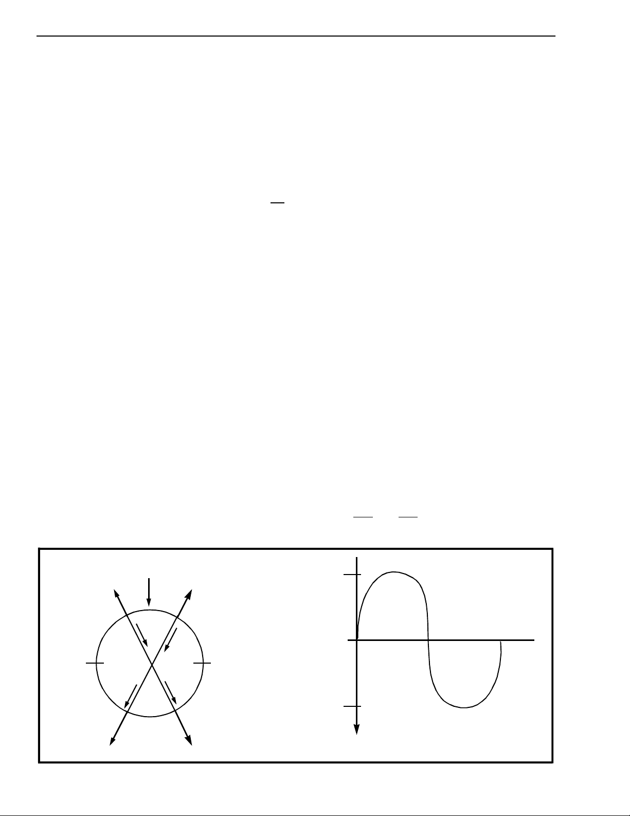
47 CH
Write
60 CH
386 Bit
Elastic
Store
34 CH
Pointer
2 CH
15 CH
28 CH
13 CH
-13 CH
Figure 7 - Elastic Bu ffer F unction al Dia gram (156 U I Wander Tolerance)
Wander Tolerance
Page 15

Preliminary Information MH89770
Elastic Buffer
The MH89770 has a two frame elastic buffer which
absorbs jitter in the received DS1 signal. The buffer
is also used in the rate conversion between the
1.544 Mbit/s DS1 rate and the 2.048 Mbit/s ST-BUS
data rate .
The received data is written into the elastic buffer
with the extracted 1.544 MHz clock. The data is read
out of the buffer on the ST-BUS side with the system
2.048 MHz clock. The maximum delay through the
buffer is 1.875 ST-BUS frames or 60 ST-BUS
channels, see Figure 7. The minimum delay required
to avoid bus content ion in the buffer memory is two
ST-BUS chan n els.
Under normal operating conditions, the system C2i
clock is phase locked to the extracted E1.5o clock
using external circuitry. If the two clocks are not
phase-locked, then the rate at which the data is
being written into the device on the DS1 side may
differ from the rate at which it is being read out on
the ST-BUS side. The buffer circuit will perform a
controlled slip if the throughput delay conditions
described above are violated. For example, if the
data on the DS1 side is being written in at a rate
slower than what it is being read out on the ST-BUS
side, the delay between the received DS1 write
pointer and the ST-BUS read pointer will begin to
decrease over time. When this delay approaches the
minimum two channel threshold, the buffer will
perform a controlled slip which will reset the internal
ST-BUS read pointers so that there is exactly 34
channels delay between the two pointers. This will
result in some ST-BUS channels containing
information output in the previous frame. Repetition
of up to one DS1 frame of information is possible.
Conversely, if the data on the DS1 side is being
written int o the buffer at a rate faster than it is being
read out on the ST-BUS side, the delay between the
DS1 frame and the ST-BUS frame will increase over
time. A controlled slip will be performed when the
throughput delay exceeds 60 ST-BUS channels. T his
slip will reset the internal ST-BUS counters so that
there is a 28 channel delay between the DS1 write
pointer and the ST-BUS read pointer, resulting in
loss of up to one frame of received DS1 data.
Figure 7 illustrates the relationship between the read
and write pointers of the receive elastic buffer.
Measuring clockwise from the write pointer, if the
read point er comes within two channels of the writer
pointer a fra me slip will o ccur, which will pu t the read
pointer 34 channels from the write pointer.
Conversely, if the read pointer moves more than 60
channels from the write pointer, a slip will occur,
which will put the read pointer 28 c hannels from the
write pointer. This provides a worst case hyst eresis
of 13 ST-BUS channels peak (26 ST-BUS channels
peak-to-peak). This can be translated into a low
frequency jitter (wander) tolerance value, accounting
for the DS1 to S T-BUS rate conversion, as f ollows:
(1.544/2.048) X 26 X 8 = 156 UI pp.
There is no loss of frame sync, multiframe sync or
any errors in the signalling bits when the device
performs a slip. The information on the FDL pins in
ESF or SLC-96 mode will, however, undergo slips at
the same time .
Framing Algorithm
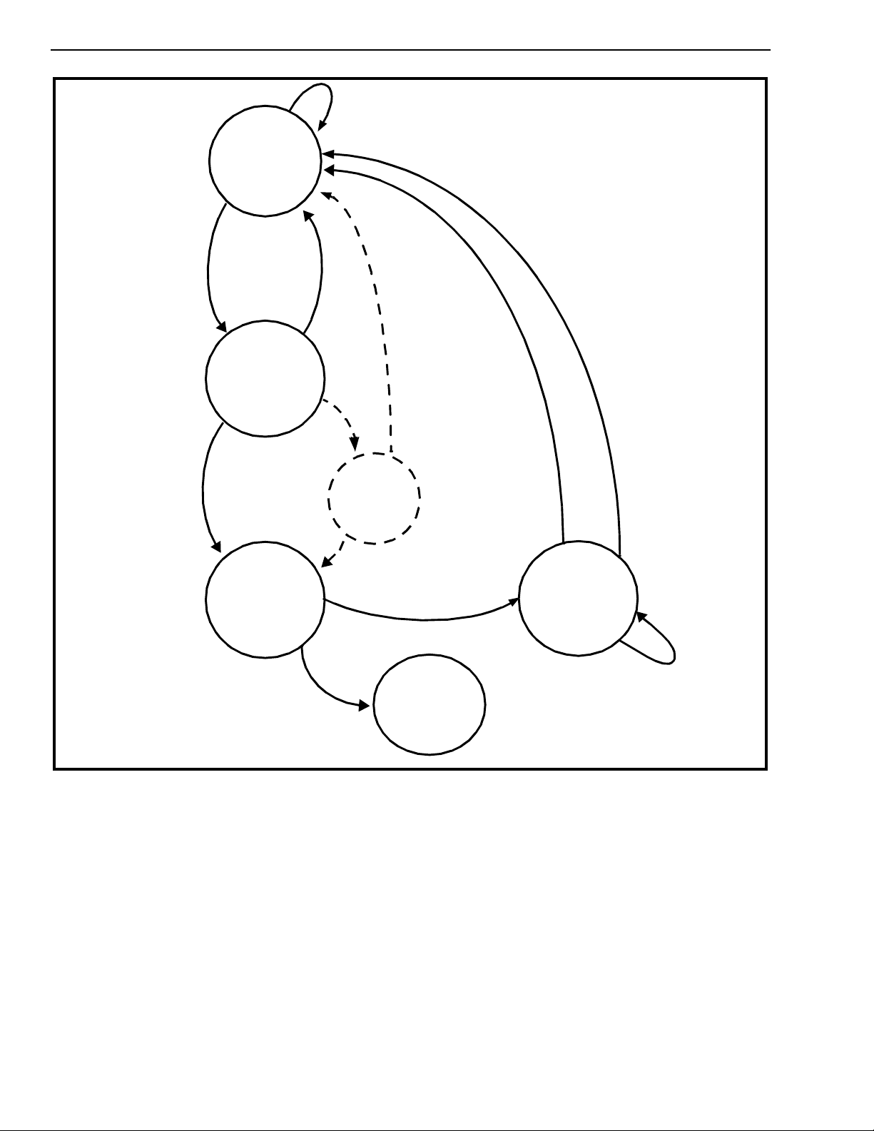
A state diagram of the framing algorithm is shown in
Figure 8. The dotted lines show whic h feature can be
switched in and out depending upon the operating
mode of the device.
In ESF mode, the framer searches for the FPS bits.
Once this pattern is detected and verified, bit 0 in
Master Status Word 1 is cleared.
When the device is operating in the D3/D4 format,
the framer searches for the F
repeating 1010... pattern in a specific bit position
every alternate frame. It will synchronize to this
pattern and declare valid terminal frame
synchronization by clearing bit 0 in Master Status
Word 1. The device will subsequently initiate a
search for the F
pattern to locate the signalling
S
frames (see Figure 21). When a correct F
has been located, bit 3 in Master Status Word 1 is
cleared indicating that the device has achieved
multiframe synchronization.
Note: the device will remain in terminal frame
synchronization even if no F
S
In D3/D4 for mat, when the C RC/MI MIC bit i n M aster
Control Word 1 is cleared, the device will not go into
synchronization if more than one bit position in the
frame has a repeating 1010.... pattern, i.e., if more
than one candidate for the terminal framing position
is located. The framer will continue to search until
only one terminal framing pattern candidate is
discovered. It is, therefore, possible that the device
may not synchronize at all in the presence of PCM
code sequences (e.g., sequences generated by
some types of test signals) w hich contain mimics of
the termin a l fra ming pattern.
pattern, i.e., a
T
pattern
S
pattern can be located.
4-139
Page 16
MH89770 Preliminary Information
False Candida te
Hunt Mode
Candidate
Candidate
Candidate
Verify
Candidate
In sync
False
CRC
Check
Candidate
Valid Candid ate
False
Candidate
*
Force d
Reframe
Out of
Sync.
Maintenance
New Frame Position
* Note: Only when in ESF mode and CRC
option is enabled.
Figure 8 - Off-L ine F ram er State D iag ram
Setting CRC/MIMIC bit high will force the framer to
synchronize to the first terminal framing pattern
detected. In standard D3/D4 applications, the user’s
system software should monitor the multiframe
synchronization state indicated by bit 3 in Master
Status Word 1. Failure of the device to achieve
multiframe synchronization within 4.5ms of terminal
frame synchronization, is an indication that the
device has framed up to a terminal framing pattern
mimic and should be forced to reframe.
One of the main features of the framer is that it
performs its function “off line”. That is, the framer
Valid Candidate
Resync
Receiver
repositions the receive circuit only when it has
detected a valid frame po sition. When the framer
exits maintenance mode the receiv e co unt ers remain
where they are until the framer has found a new
frame position. This means that if the user forces a
reframe when the device was really in the right
place, there will not be any disturbance in the circuit
because the framer has no effect on the receiver
until it has found synchronization.
The out of
synchronization criterion can be controlled by bit 0 in
Master Control Word 2. This bit changes the out of
frame conditions for the maintenance state.
4-140
Page 17
Preliminary Information MH89770
A
A
A
A
A
A
A
A
A
A
A
A
A
A
A
A
A
A
A
A
A
A
A
A
A
A
A
A
A
A
A
A
A
A
A
A
A
A
A
A
A
A
A
A
A
A
A
A
A
A
A
A
A
A
A
A
A
A
A
A
A
A
A
A
A
A
A
A
A
A
A
A
A
A
A
A
A
A
A
A
A
A
A
A
A
A
A
A
A
A
A
A
A
A
A
A
A
A
A
A
A
A
A
A
A
A
A
A
A
A
A
A
A
A
A
A
AAA
AAA
AAA
AAA
AAA
50
Percentage Reframe Time Probability Versus Reframe Time
A
A
40
%
30
A
A
20
10
0
A
A
A
A
A
A
A
A
A
A
A
A
A
A
A
A
A
A
A
A
A
A
A
A
A
A
A
A
A
A
A
A
A
A
A
A
A
A
A
A
A
A
A
A
A
A
A
A
A
A
A
A
A
A
A
A
A
A
A
A
A
A
A
A
A
A
A
A
A
A
A
A
A
A
A
A
A
A
A
A
A
A
A
A
A
A
A
A
A
A
A
A
A
A
A
With Pseudo Random Data
A
A
A
A
A
A
A
A
A
A
A
A
A
A
A
A
A
D4
ESF
078 10 12 1416 1820222426 28 3032 34
Reframe Time (ms)
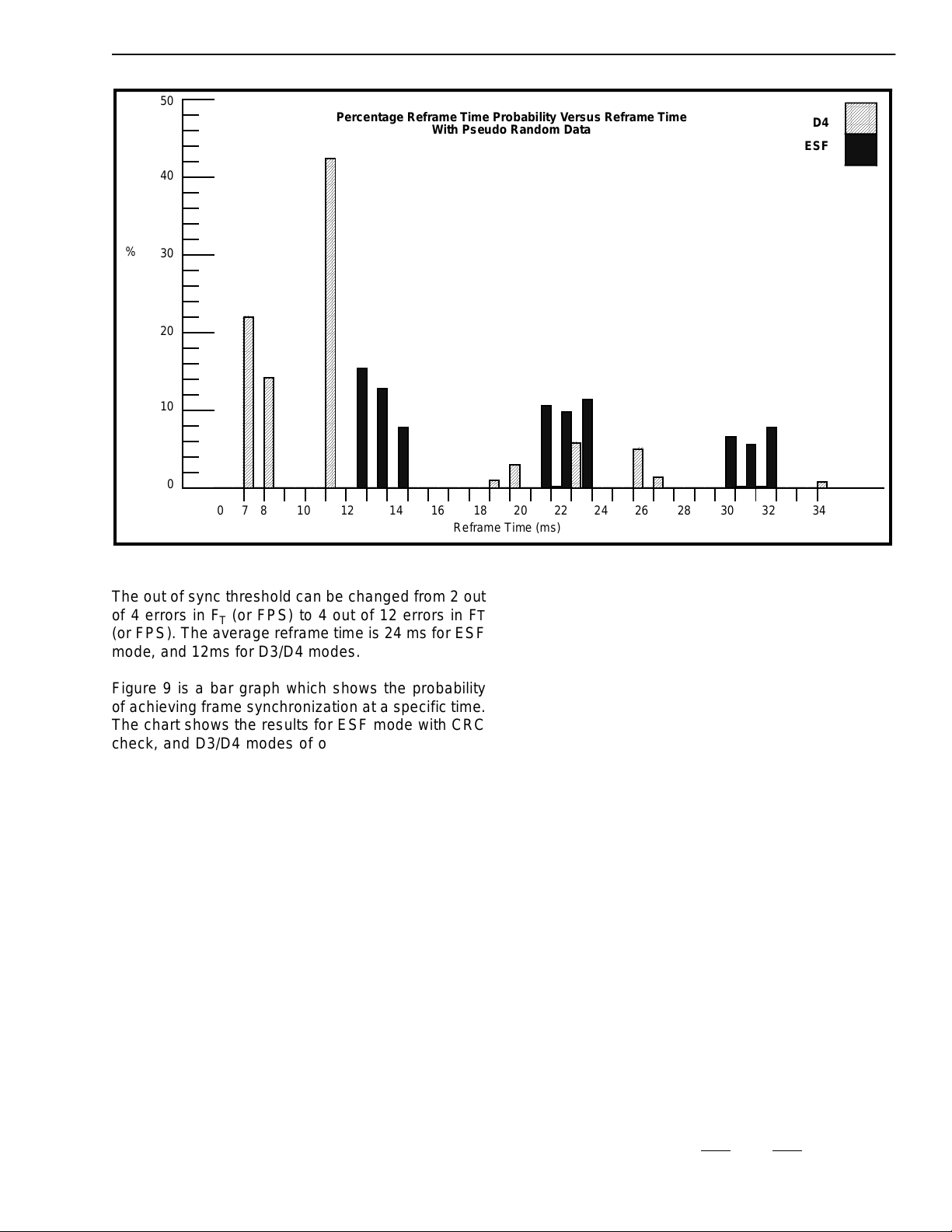
Figure 9 - Reframe Time
The out of sync threshold can be changed from 2 out
of 4 e rro rs i n F
(or FPS) to 4 out of 12 errors in FT
T
(or FPS). The average reframe time is 24 ms for ESF
mode, and 12ms for D3/D4 modes.
application to illustrate how the data on the FDL
could be used. The digital phase-locked loop, the
MT8941, provides all the clocks necessary to make
a functional interface. The 1.544 MHz clock
extracted by the MH89770 is used to clock in data at
Figure 9 is a bar graph which shows the probability
of achieving frame synchronization at a specific time .
The chart s hows th e res ults fo r ESF m ode with CRC
check, and D3/D4 modes of operation. The average
reframe ti me with random d at a is 2 4 ms for ESF, a n d
RxT and RxR. It is also int ernally divided by 193 to
obtain an 8 kHz clock which is output at E8Ko. The
MT8941 uses this 8 kHz signal to provide a phase
locked 2.048 MHz clock for the ST-BUS interface
and a 1.544 MHz clock f or the DS1 transmit side.
13 ms for D3/D4 modes. The probability of a
reframe tim e of 35 ms or less is 88% for ESF
mode, and 97% for D3/D4 modes. In ESF mode it is
recommended that the CRC check be enabled
unless the line has a high error rate. With the CRC
check disabled the average refram e time is greater
because th e fram e r mu st also check fo r mi mi c s.
Applications
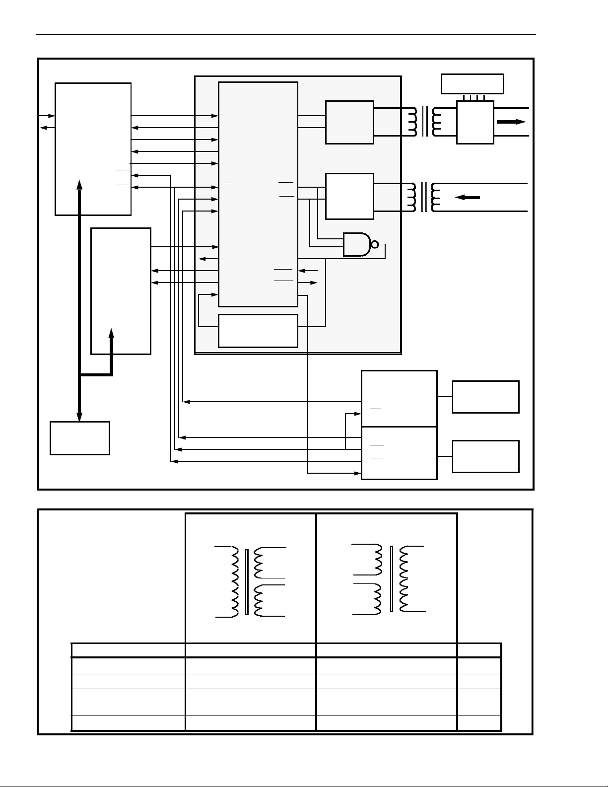
1. Typical T1 Application
Figure 10 shows the external components that are
required in a typical T1 application using the
MH89770. The MT8980 is used to control and
monitor the device as well as
DSTo (refer to Application Note MSAN-123 for more
information on the operation of the MT8980). The
MT8952, HDLC protocol controller, is shown in this
switch data to DSTi and
Note: the configurations shown in Figures 10 and 12
using the MT8941 may not meet specific jitter
performance requirements. A more sophisticated
PLL may be required for applications designed to
meet specific standards. Please refer to the MT8941
data sheet for further details on its jitter performance.
The split phase unipolar signals output by the
MT8977 at TxA and TxB are used by the line driver
circuit to generate a bipolar AMI signal. The line
driver is transformer coupled to an equalization
circuit and the DS1 line. Equalization of the
transmitted signal is required to meet AT & T
specifications for crossconnect compatible
equip-ment (see AT&T Technical Advisory #34).
Specifica-tions for the input and output transformers
are shown in Figure 11. On the receive side the
bipolar line signal is converted into a unipolar format
by the line receiver circuit. The resulting split phase
signals are input at the RxA
and RxB pins on the
4-141
Page 18
MH89770 Preliminary Information
MH89770
DIP SWITCH
STi3
STo3
MT8980
STo0
STi0
STo1
STi1
STo2
C4i
F0i
•
DSTi
DSTo
CSTi0
CSTo
CSTi1
F0i
C2i
C1.5i
MT8977
TxA
TxB
RxA
RxB
Tx
Line
Driver
RX
•
•
Line
Receiver
OUTA
EQU
OUTB
MH89761
RxT
RxR
Micro
Processor
MT8952
CDSTo
CDSTi
Cki
TxFDL
TxFLDClk
RxFDL
RxFDLClk
E1.5i
CLOCK
EXTRACTOR
RxD
TxSF
RxSF
E8Ko
•
1.544 MHz
•
CVb
F0i
C2o
F0b
C4b
C8Kb
Figure 10 - Typical ESF Configuration
MT8941
12.352 MHz
Osc.
16.384 MHz
Osc.
4-142
•
MH89770
•
•
3
O
6
O
4
O
O
5
Line Side
O
1
8
O
Parameter Input Transfo rme r Output Transformer Units
MH89770
1
O
5
O
O
2
6
O
•
•
Line Side
•
4
O
8
O
Line Impedance 100 100 Ω
Inductance (1-8) >2.2 (4-8) 0.46 m H
Turns R at i o (1-8): (3-6) 1 :1
(1-8):(4-5) 1:1
(1-5):(4-8) 1.89:1
(2-6):(4-8) 1.89:1
Isolation 1500 1500 V(rms)
Figure 11 - Typical Parameters of the Input and Output Transformers
Page 19
Preliminary Information MH89770
High Speed
Parallel
Telecom Bus
Signalling and
Link Control
BUS
MT8920B
(Mode 2)
D
0-D7
A0-A
5
CS
R/W
OE
MMS MS1 24/32
MT8920B
(Mode 1)
D0-D
7
A0-A
5
CS
DS
R/W
DTACK
IRQ
IACK
STo0
STo1
+5V
STo0
STi0
STo1
MMS
+5V
STi0
C4i
F0i
C4i
F0i
MH89770
MT8977
DSTi
DSTo
CSTi0
CSTo
CSTi1
•
F0i
C2i
C1.5i
E1.5i
CLOCK
EXTRACTOR
TxA
TxB
RxA
RxB
RxD
E8Ko
•
Tx
Line
Driver
Rx
•
Line
Driver
•
OUTA
OUTB
RxT
RxR
DIP
SWITCH
EQU
MT89761
•
•
1.544 MHz
•
CVb
F0i
C2o
F0b
C4b
C8Kb
MT8941
12.352 MHz
Osc.
16.384 MHz
Osc.
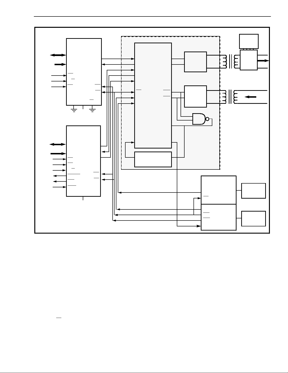
Figure 12 - Usin g the MH8 97 70 in a P arallel Bus En viro nme nt
MT8976. The signals are combined to produce a
composite return t o zero signal which is clocked into
the MT8976 at RxD.
2. I nter facing the MH 89770 to a P aral lel Bus
The MH89770 can be interfaced to a high speed
parallel bus or to a microprocessor using MT8920B
Parallel Access Circuit (STPA). Fig. 12 shows the
MT8977 interf aced to a parallel bus structure using
two STPA’s operating in modes 1 and 2.
The first STPA operating i n m o de 2 (MMS= 0,
MS1=1, 24
/32=0), routes data and/or voice
information between the parallel telecom bus and the
T1 or CEPT link via DSTi and DSTo. The second
STPA, operating in mode 1 (MMS=1) provides
access from the signalling and link control bus to the
MH89770 status and control channels. All signalling
and link functions may be controlled easily through
the STPA transmit RAM’s Tx0, Tx1, while status
information is read at receive RAM Rx0. In addition,
interrupts can be set up to notify the system in case
of slips, los s o f sync, alarms, violations, e tc.
3. P CM/Voice Channel Bank
The D3/D4 channel bank is one of the most widely
used pieces of equipment in the North American
network today. The D3/D4 channel converts 24
analog telephone lines into the 24 channels of a T1
serial stream. The channel bank is the interface point
between a digital switching or transmission system
and the analog telephone loop. The industry is
moving towards end-to-end digital connections
(ISDN), but the analog channel bank will still be in
use for many yea rs to come.
4-143
Page 20
MH89770 Preliminary Information
Analog Line Interface
CTLi
OFHK
PCMi
•
•
PCMo
•
•
•
•
•
MUX
•
•
•
SLIC #1
T
R
•
•
•
•
SLIC #24
T
R
Shift
•
Reg.
Shift
Reg.
CTLo
OFHK
Signalling Interface
MT8870
STD
#1
D3
Do
•
•
•
MT8870
STD
#N
D3
Do
MT8964
#1
•
•
•
MT8964
#N
PCMi
Switch Matrix
STo0
•
STi0
•
STo3
STi3
F0i
C4i
MT8980
µP
C1.5i
STo1
STi1
STo2
STi2
STo4
F0i
C4i
C2i
DSTi
DSTo
CSTi0
CSTo
CSTi1
C2i
F0i
C1.5i
CVb
F0i
F0b
•
C4b
C2o
T1 Interface
MH89770
OUTA
MT8941
DPLL#1
DPLL#2
C8Kb
C16i
OUTB
RxT
RxR
E8Ko
C12i
Equal-
izer
12.352
MHz Osc.
16.384
MHz Osc.
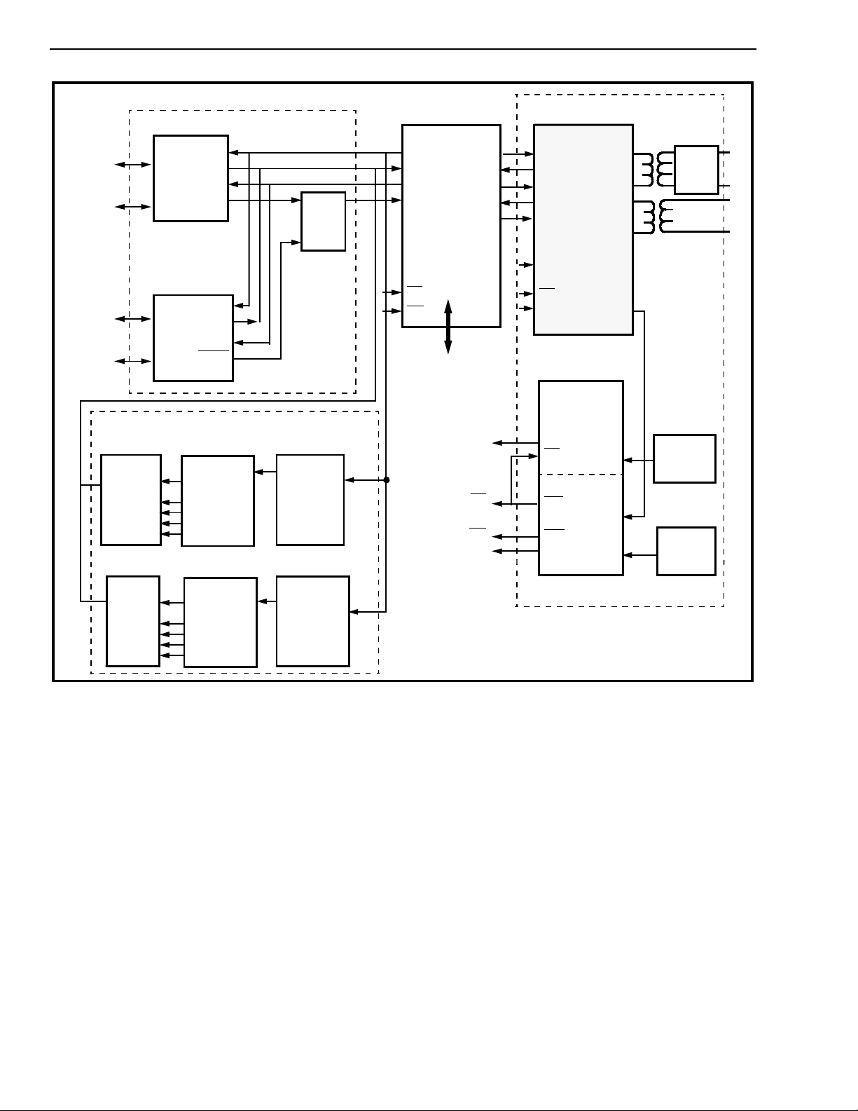
Figure 13 - PCM/Voice Data Channel Bank
Figure 13 shows a block diagram of a channel bank
that has been divided into four sections, the analog
line interface, signalling interface, switch matrix, an d
T1 interface. The subscriber line interface circuit
(SLIC) provides interface to the telephone line, i.e.,
provides loop current and ringing voltage, and
converts the analog voice signal into µ-Law PCM.
The SLIC also detects the off-hook condition for
conventional POTS (Plain Old Telephone Set)
signalling.
Once the voice is encoded into digital format the
switch matrix transfers the 24 consecutive channels
that are received from the SLICs to the 24 valid
channels used by the MH89770. The MH89770
formats and transmits this information on the T1 line.
Signalling information from the telephone sets can
be routed straight through to the output T1 channel,
or it can be r o ut ed to th e DTMF receiver p ool . T h is is
4-144
easily accomplished by the MT8980 switch matrix
once the SLIC has digitized the analog signal.
Channel banks must be able to operate in a loop
timed mode so that they meet the clock
synchronization requirements of a level four entity.
Phase-locked loop #2 of the MT8941 generates the
ST-BUS clocks that are synchronized to the
extracted 8kHz clock, and phase-locked loop #1
generates the transmit T1 clock synchronized to the
ST-BU S.
4. ISDN Voice/ D ata C h anne l Bank/Con centr ator
The ISDN channel bank is a term that is used in this
context to describe a system that performs the same
logical function as the D3/ D4 channel bank. That is,
it concentrates the subscribers digital loop into the
primary dig i ta l transmission s ch e m e , th e T1 tr u n k.
Page 21
Preliminary Information MH89770
Digital Line Interface
MT8910
DSTo
DSTi
Z
T
•
•
•
•
•
•
•
•
•
•
•
•
•
•
MT8910
DSTo
Z
T
DSTi
Switch Matr ix
MT8980
µP
STo1
STi1
STo2
STi3
STo3
•
•
DSTo
DSTi
•
•
DSTo
•
•
DSTi
STi0
STo0
C4i
F0i
D-Channel Processing
MT8952 MT8952
•
T1 Interface
MH89770
DSTi
DSTo
CSTi0
CSTo
CSTi1
C2i
F0i
C1.5i
F0i
OUTA
OUTB
E8Ko
MT8941
Equal-
izer
RxR
RxT
C1.5
•
•
•
•
MT8952
µP
µP
E8Ko
F0o
•
C2o
C4o
DSTo
DSTi
Figure 14 - ISDN Voice Data Channel Bank
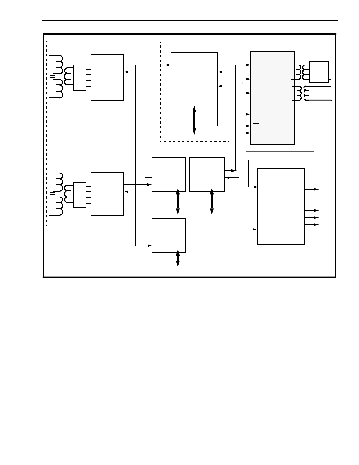
The ISDN channel bank in Figure 14 is divided into
four blocks, the digital line interface, the switch
matrix, the D channel processing, and the T1
interface. Beginning with the digital line interface, the
MT8910 provides 2B+D 160k bit bidirectional
communication over single twisted pair wiring. The
MT8910 converts the 160kbit line signal into ST-Bus
format, where it can be manipulated by the MT8980
switch matrix. The data received from the MT8910 is
then transferred to the D channel processor by the
switch matrix. The D channel processor converts the
2B+D format used on the 160 kBit digital line into the
23B+D format used on the T1 Link.
To control and monitor the MT8910s and the T1
interface the switch matrix operates some of its input
and output streams in m essage mode. This enables
the system to control all of the functions of the
MT8910s and the T1 interface through the Control
ST-BUS points, (CSTi/o).
µP
Clock synchronization is done by the MT8941.
Phase-locked loop # 2 generates ST-BUS clocks that
are synchronized to the extracted 8kHz output from
the T1 interface. Phase-locked loop #1 generates
the transmit T1 clock synchronized to the ST-BUS
clocks, which are synchronized to the extracted T1
clock. This scheme will also allow the system to
operate in a loop timed mode.
With appropriate multiplexing a single D channel
processor can handle all 23 2B+D interfaces. If both
B channels on all 24 lines are going to be used then
it would be necessary to use two T1 trunk interfaces.
4-145
Page 22
MH89770 Preliminary Information
AAAA
AAAA
AAAA
AAAA
5. Di gital Ac ces s Cross Co nn ect Sy stem
(DACS)
The Digital Access Cross Connect System (DACS) is
a T1 switch with 127 T1 lines as input and output
plus one T1 line that is reserved for test and
maintenance purposes. A DACS is capable of
switching any input channel on any T1 trunk to any
output channel on any T1 trunk.
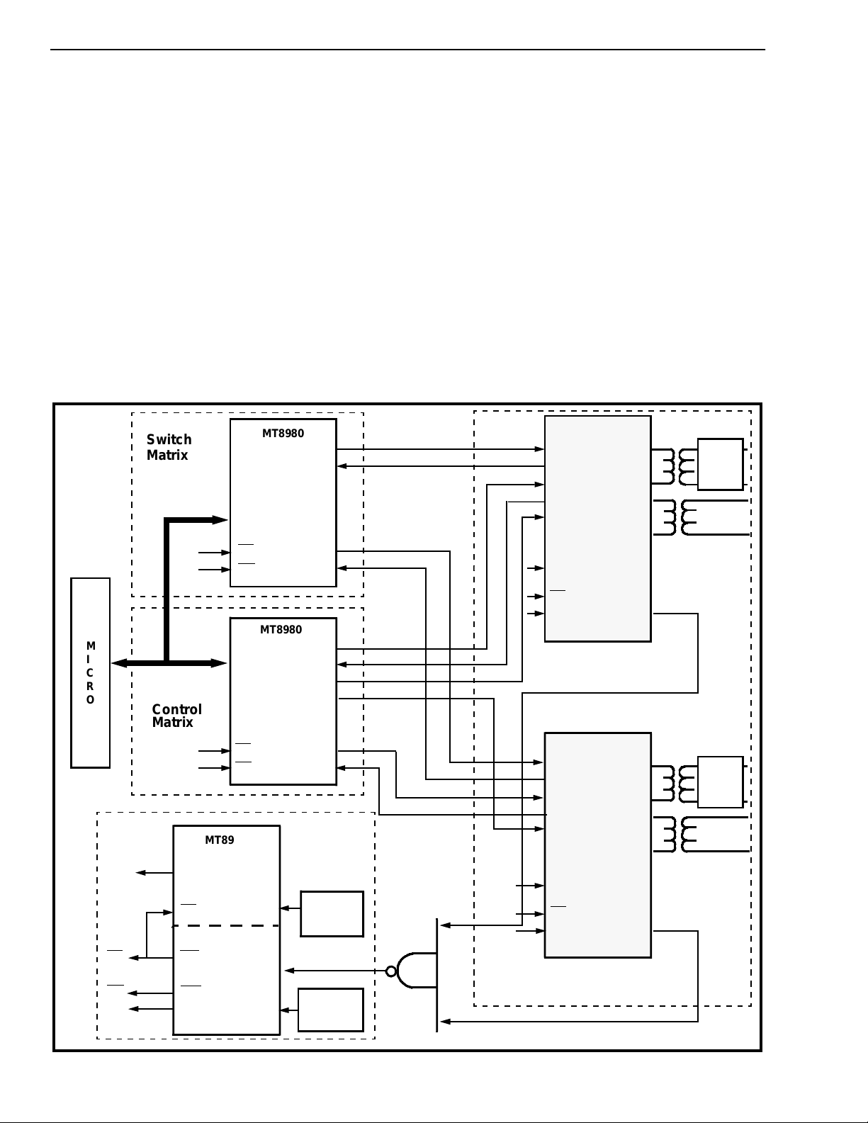
There are four main blocks in Figure 15, the T1
interfaces, the switch matrix, the control matrix, and
the clock generator. The digital trunk interface is
made up of the MH89770 plus the additional
components required to interface to the transmission
line. The MH89770 handles all of the required
transmit and receive data formatting, and converts
the 1.544 MHz serial stream into ST-BUS format so
F0i
C4i
MT8980
STo0
STi0
STo7
STi7
Switch
Matrix
that it can be routed through the MT8980
synchronous switch matrix.
The switch matrix can be built so that the m aximum
throughput delay is 1 frame +2 channels. The switch
matrix will not only route data channels to their
destination, but it will also route the received
signalling bits through to the destination channel.
This is necessary because the receiving MH89770
decodes the T1 stream, and the transmitting
MH89770 has to reconstruct the outgoing T1 stream.
In other words, there is no multiframe integrity
between received data and transmitted data. The
total throughput delay is one frame plus ten ST-BUS
channels for the MH89770 receiver, 2.5 ST-BUS
channels for the MH89770 transmitter, and one
frame plus two ST-BUS channels for the switch
matrix for a total of 2.5 frames worst case.
MH89770
DSTi
DSTo
CSTi0
CSTo
CSTi1
C2i
OUTA
OUTB
RxT
RxR
Equal-
izer
F0i
MT8980
M
I
C
R
O
Control
STo0
STi0
STo1
STo2
C1.5i
Matrix
MH89770
DSTi
DSTo
CSTi0
CSTo
CSTi1
C2i
F0i
C1.5i
T1 Interfaces
C1.5i
F0i
C4i
C2i
CVb
F0i
F0b
C4b
C20
MT8941
DPLL #1
DPLL #2
F0i
C4i
C12i
C8Kb
C16i
STo7
STi7
Clock
Generator
12.352
MHz Osc.
16.384
MHz Osc.
•
•
•
•
•
•
•
E8Ko
•
•
•
•
•
•
OUTA
OUTB
RxT
RxR
E8Ko
Equal-
izer
4-146
Figure 15 - Digita l Access Cro ss Connect S ystem (DACS)
Page 23
Preliminary Information MH89770
Asynchronous
Interface
ACIA
R
S
2
3
2
R
S
2
3
2
R
S
2
3
2
D0-D
A
ACIA
D0-D
A0-A
ACIA
D0-D
A0-A
0-A7
•
•
•
Protocol Converter
•
•
MT8952
D
0-D7
A0-A
MT8952
D0-D
A0-A
MT8952
D0-D
A0-A
7
7
7
7
7
7
Micro
7
•
7
68008
•
•
•
7
7
•
•
•
•
•
•
•
•
Switch Matri x
STi0
•
STo0
•
F0i
C4i
•
•
•
•
•
MT8980
C1.5i
STo1
STi1
STo2
STi2
STo3
F0i
C4i
C2i
DSTi
DSTo
CSTi0
CSTo
CSTi1
C2i
F0i
C1.5i
CVb
F0b
•
C4b
C20
T1 Interface
MH89770
MT8941
DPLL #1
DPLL #2
OUTA
OUTB
RxT
RxR
E8Ko
C12iF0i
C8Kb
Equal-
izer
12.352
MHz
Osc.
16.384
MHz
Osc.
•
Figure 16 - Digital Multiplex Interface (DMI)
The control block only interfaces with the switch
matrix. Besides routing channels and signalling
through to the proper destination, the switch matrix
must also supply the Master Control Words, and
monitor the Master Status Words for each MH89770.
The clock generation block supplies the ST-BUS
clocks and the T1 transmit clocks that are
synchronized to one of the T1 trunks. All of the
extracted 8 kHz outputs are NANDed together before
they are input to PLL #2 of the MT8941.
Phase-locked Loop #2 of the MT8941, will generate
ST-BUS clock signals for the MH89770s and the
MT8980s that are synchronize d with the chosen T1
line. The E8Ko of all of the other MH89770s can be
tristated from t he M aster C on trol Word , whi ch al lows
the system controller to select any one of 128 T1
lines to act as the synchronization source. By
connecting the frame pulse output, F0o
F0i
of PLL # 1, the MT8941 will generate the T1
, of PLL #2 to
transmit clock that is phase-locked to F0o
, which in
turn is phase-locked to the master synchronization
signal, E8Ko. If all of the T1 trunks are from the
network any short term differences in the received
data rate will be absorbed by the elastic buffer in the
MH89770.
6. Digital Multiplex Interface (DMI)
Figure 16 illustrates an imp lementation of the Digital
Multiplex Interface (DMI) specification, which defines
a computer to PBX interface. This interface can
convert 300 baud to 64 kbaud asynchronous or
synchronous data channels to T1 format with clear
channel capabilities and common channel signalling.
Figure 16 is broken down into four functional blocks
which are the asynchronous interface (ACIAs), the
protocol convert er (micro and MT8952s), the switch
matrix (MT8980), and the T1 interface (MH89770).
4-147
Page 24
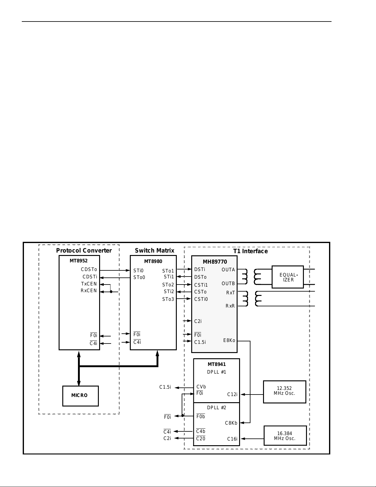
MH89770 Preliminary Information
The Asynchronous Communications Interface
Adapters (ACIA) provide a standard RS232 interface
that is compatible with many off-the-shelf modems
and data sets. A single microprocessor is capable of
handling the protocol conversion between the RS232
ports and the MT8952 HDLC protocol controller.
The MT8952 interfaces directly to the ST-BUS, which
in turn interfaces directly to t he T1 interface devices.
Instead of the MT8952 operating at 64 kbit/s
continuously, it operates at 2.048 Mbit/s and
inputs/outputs an 8 bit burst every 125 µsec. This
feature eliminates the need for an additional rate
conversion circuit to m ult iplex the HDLC outputs up
to the T1 data rate. Each of the HDLC chips is
assigned a timeslot on the ST-BUS in a manner that
is similar to enabling a voice codec. When the
MT8952 is not enabled the output driver is tristated.
The channel assignment circuit is therefore very
simple. The switch matrix, in the message mode,
passes monitor and control information between the
microprocessor and the T1 interface over ST-BUS
stream 0. The MT8980 is also used to reformat the
ST-BUS data streams between the protocol
converter and the MH89770 int erface.
The MH89770 and the MT8941 form the T1
interface. The MH89770 convert s the data received
on the ST-BUS into a 1.544 MHz T1 stream. All of
the formatting and decoding of the T1 signal is
performed by this device. The MT8941 provides the
clock synchronization required to operate in a loop
timed mode. Digital phase-locked loop #2 provides
ST-BUS clocks that are synchronized to the
extracted 8kHz, and digital phase-locked loop #1
provides the transmit 1.544 MHz clock synchronized
to the ST-BUS.
7. High Speed Data Transmission Link
High speed data links are becoming increasingly
popular in private networks and computer
communications. The basic mode of transmission is
to assemble data into packets (e.g., HDLC or
ethernet) which are transported on a T1 link
configured as a 1.536 Mbit/s serial channel. No T1
repeaters are required if the transmission link length
is 1300 ft. or less (e.g., business complex or
university). However, if the t ransmission link length is
greater than 1300 ft., a repeatered T1 line must be
leased from the local telephone operating company.
Protocol Converter
MT8952
CDSTo
CDSTi
TxCEN
RxCEN
F0i
C4i
MICRO
Switch Matrix
MT8980
STi0
STo0
•
F0i
C4i
STo1
STi1
STo2
STi2
STo3
C1.5i
F0i
C4i
C2i
•
MH89770
DSTi
DSTo
CSTi1
CSTo
CSTi0
C2i
F0i
C1.5i
MT8941
DPLL #1
CVb
F0i
DPLL #2
F0b
C4b
C20
T1 Interface
OUTA
OUTB
RxT
RxR
E8Ko
C12i
C8Kb
C16i
EQUAL-
IZER
12.352
MHz Osc.
16.384
MHz Osc.
4-148
Figure 17 - Hig h Spee d D ata Transmissio n Link
Page 25
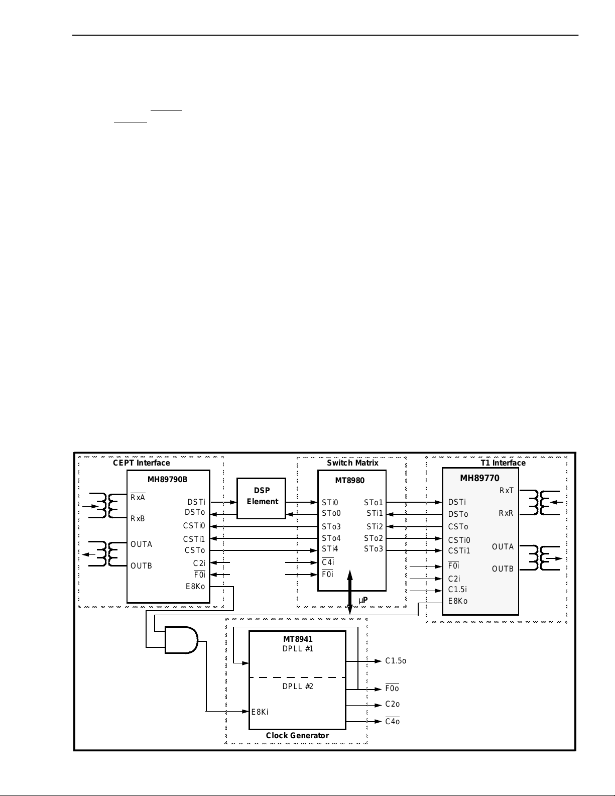
Preliminary Information MH89770
Figure 17 is divided into three functional blocks
which are the protocol converter, switch matrix, and
T1 interface. The protocol section is dependent on
the particular format that is chosen. In this example it
is assumed that the protocol is HDLC. The Transmit
Clock Enable (TxCEN) and the Receive Clock
Enable (RxCEN
) of the MT8952 are active for a
period of 24 co nsecutive ST-BUS channels, and the
clock speed is 2.048 MHz. This enables the protocol
conversion section to interface directly to the switch
matrix. The switch matrix switches the first 24
channels received from the protocol section into the
24 valid timeslots used by the MH89770. Once the
data enters the T1 interface the MH89770 formats
and transmits the data on the T1 line.
Control and monitoring of the T1 interface is done
through the MT8980 switch matrix. CSTi0 and
CSTo1 are connected to the ST-BUS streams that
are configured for message mode so the controlling
microprocessor can access the Master Control
Words and the Master Status Words.
The received portion of the T1 interface extracts the
data from th e T1 stream an d formats it into ST-BUS
channels. The MT8980 switches these ST-BUS
channels into the first 24 consecutive channels of an
ST-BUS stream, which is passed to the protocol
conversion block. HDLC packets are disassembled
from the incoming S T-BUS stream by the MT8952.
Clock generation and synchronization are handled
by the MT8941. DPLL #2 generates ST-BUS cloc ks
that are phase-locked to the extracted 8KHz, and
DPLL #1 generates the transmit T1 clock that is
phase-locked to the ST-B US frame pulse. Therefore,
the interface is operating in a loop timed mode and
there will be no loss of information due to slips. The
MT8941 can also be configured to operate in a
master timing mode.
8. T1 to CEPT Digital Trunk Converter
The two main digital trunk transmission formats in
use today are T1 and CEPT. Mitel's T1 and CEPT
interfaces convert the digital trunk format into
ST-BUS format. The common element between the
two systems is the ST-BUS. Therefore, a T1 to
CEPT digital trunk converter can be realized.
Figure 18 shows five blocks which are the T1
interface, switch matrix, CEPT interface, clock
generation and synchronization, and DSP Element.
The T1 interface converts the 1.544 MHz serial
stream into the ST-BUS format which interfaces to
the switch matrix through DSTi and DSTo. The CEPT
interface converts the 2.048 MHz serial stream into
the ST-BUS format and interfaces to the switch
matrix through the DSP element.
CEPT Interface
MH89790B
RxA
RxB
OUTA
OUTB
DSTi
DSTo
CSTi0
CSTi1
CSTo
C2i
F0i
E8Ko
DSP
Element
E8Ki
Clock Generator
MT8941
DPLL #1
DPLL #2
Switch Matrix T1 Interface
MH89770
DSTi
DSTo
CSTo
CSTi0
CSTi1
F0i
C2i
C1.5i
E8Ko
RxT
RxR
OUTA
OUTB
STi0
STo0
STo3
STo4
STi4
C4i
F0i
MT8980
STo1
STi1
STi2
STo2
STo3
µP
C1.5o
F0o
C2o
C4o
Figure 18 - T1 to CEPT Digital Trunk Converter
4-149
Page 26

MH89770 Preliminary Information
With both the T1 data and the CEPT data converted
to the ST-BUS format, the two digital trunks can
exchange information through the switch matrix.
Unfortunately, the signalling information from the tw o
formats is not exchanged as easily. The T1 A and B
signalling bits must be read by the controlling
microprocessor and converted in software to the
CEPT ABCD signalling bits, and vice versa. The
circuit must also convert all the channels carrying
voice data to the appropriate encoding scheme, (i.e.,
T1 µ-Law or CEPT A-Law). This is done by the block
labelled DSP in Figure 18, Digital Signal Processor.
The final component of the system is the MT8941.
The extracted 8 kHz outputs from the T1 and the
CEPT interfaces are combined with an AND gate
before being connected to the MT8941. One of the
interfaces is selected as the synchronization source
by enabling its output through the Master Control
Word of the chosen interface. Phase-locked loop #2
will then generate ST-BUS clocks that are
synchronized to either the T1 network or the CEPT
network. Phase-locked loop #1 is configured to
generate the T1 transmit clock synchronized to the
ST-BUS. Therefore, i f th e S T-BUS is synch ro n ize d to
one network then the elastic buffer in the opposite
interfaces will perform controlled slips between that
network a n d th e T 1 to CE PT co n ve rt er.
Packaging
The MH89770 is available in two package options
which are:
• The MH897 70S w hi ch is a s urface moun table
version of t he MH8 9770N is sui table for
Infrared Reflow (I.R.) soldering. See Figure 35
for the dimensional drawing, and Figure 36 for
the recomm ende d foo tprint.
• The MH897 70N has a row p itch o f 0.8”. See
Figure 37 for the dimensional drawing for this
part.
Magnetics Inf or mation
For supporting initial design activities, Mitel
Semiconductor has available the MH89770 Magnetic
Kit which contains the magnetics shown in Figure 11.
Alternatively, they are available directly from the
following manufacturer:
Fil tr an Lt d .
229 Colonnade Road
Nepean, O n ta r i o
Canada K2E 7K3
Telephone: (613) 226-1626
Please refer to Figure 6 for the transformer part
numbers.
4-150
Page 27

Preliminary Information MH89770
Absolute Maximum Ratings*
Parameter Symbol Min Max Units
1 Supply Voltage with respect to V
SS
V
DD
2 Voltage on any pin other than supplies, O U TA or OUTB V
3 Voltage on OUTA or OUTB 15 V
4 Current at any pin other than supplies, OUTA o r OUTB 20 mA
5 Current at OUTA or OUTB 200 mW
6 Storage Temperature T
* Exceeding these values ma y cause perm anen t dama ge. Functi onal operati on und er these cond ition s is not implied.
ST
Recommended Operating Conditions - Voltages are with respect to ground (V
Parameters Sym Min Typ‡Max Units Test Conditions
1
Operating Temperature T
OP
I
2 Supply Voltage V
n
p
3 Input High Voltage V
u
t
s
4 Input Low Voltage V
‡ Typical figures a re at 25°C and are for desi gn aid only: not guarantee d and not subje ct to producti on testing.
DD
IH
V
IH
IH
V
IL
070°C
4.5 5.0 5.5 V
2.4 V
DD
3.0 V Line Inputs
V
SS
0.4 V Digital Inputs
0.3 V Line Inputs
-0.3 7 V
-0.3 VDD+0.3 V
SS
-20 85 °C
) unless otherwise stated.
SS
V Digital Inputs
.
DC Electrical Characteristics - Clocked operation over recommended temperature ranges.
Parameters Sym Min Typ‡Max Units Test Conditions
1
2 Input High Voltage V
3 Input Low Voltage V
4 Input Leakage Current I
5
6 Output Low Cu rren t I
7 Output Low Voltage
8 Input Impedance RxT to RxR
9 Schmitt Trigger Input (XSt) V
‡ Typical figures a re at 25°C and are for desi gn aid only: not guarantee d and not subje ct to producti on testing.
Supply Current I
I
n
p
u
t
s
Output High Current I
O
u
t
p
u
t
s
OUTA or OUTB
RxT or RxR to Gnd
DD
2.0 V Digital In puts
IH
IL
IL
OH
OL
V
OL
Z
IN
T+
V
T-
7 20 mA Sour ce Current VOH=2.4V
2 10 mA Sink Current VOL=0.4V
1.5 V
12 25 mA Outputs Unloaded
0.8 V Digit al In puts
±1 ±10 µA Digit al In puts VIN=0 to V
0.25 V IOL=10mA
400 Ω
1K Ω
4.0 V
AC Electrical Characteristics† - Capacitance
Characteristics Sym Min Typ‡Max Units Test Conditions
DD
1 Input Pin Capacitance C
2 Output Pin Capacitance C
† Timing is over recomm end ed temperatu re & powe r suppl y volt age s.
‡ Typical figures a re at 25°C and are for desi gn aid only: not guarantee d and not subje ct to producti on testing.
I
O
10 pF
10 pF
4-151
Page 28
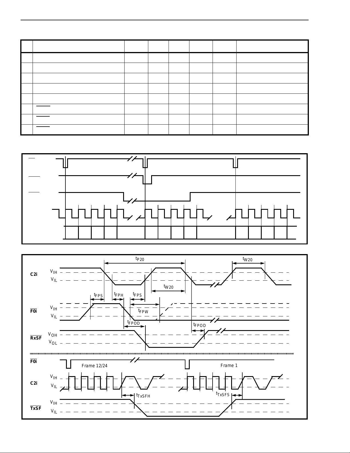
MH89770 Preliminary Information
AAAA
AAAA
AAAA
AAAA
AAAA
AAAA
AAAA
AAAA
AAAA
AAAA
AAAA
AAAA
AAAA
AAAA
AAAA
AAAA
AAAA
AAAA
AAAA
AAAA
AAAA
AAAA
AAAA
AAAA
AAAA
AAAA
AAAA
AAAA
AAAA
AC Electrical Characteristics† - Clock Timing (Figure 19 & 20)
Characteristics Sym Min Typ
‡
Max Units Test Conditions
1 C2i Clock Period t
2 C2i Clock Width High or Low t
3 Frame Pulse Setup Time t
4 Frame Pulse Hold Time t
5 Frame Pulse Width t
6 RxSF
7 TxSF
8 TxSF
NB: Fram e Pu ls e is repeate d every 125µs in synchronization with the clock.
† Timing is over recommended temperature & power supply voltages.
Output Delay t
Hold Time t
Setup Time t
p20
W20
FPS
FPH
FPW
FPOD
TxSFH
TxSFS
400 488 600 ns
200 244 300 ns t
50 ns
50 ns
50 ns
125 ns 50pF Load
0.5 124. 5 µ s
0.5 124.5 µs
‡ Typical figures are at 25°C and are for design aid only: not guarantee d and not subje ct to producti on testing.
F0i
Fram e 12/24
Frame 1
RxSF
TxSF
C2i
= 488 ns
P20
Frame 2
ST-BUS
BIT CELLS
C2i
F0i
RxSF
F0i
C2i
TxSF
Bit7Bit6Bit5Bit
4
Bit7Bit6Bit5Bit
4
4
Bit7Bit6Bit5Bit
Figure 19 - C lock & F ram e Alignm ent for ST-BUS Streams
t
P20
V
IH
V
IL
t
W20
FPH
t
t
FPOD
FPS
t
t
TxSFH
FPW
t
FPOD
Frame 1
t
TxSFS
t
FPS
V
IH
V
IL
V
OH
V
OL
t
Fram e 12/24
V
IH
V
IL
V
IH
V
IL
t
W20
4-152
Figure 20 - Clock & Frame Pulse Timing for ST-BUS Streams
Page 29
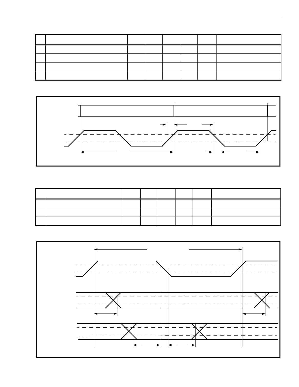
Preliminary Information MH89770
AC Electrical Characteristics† - Timing For DS1 Link Bit Cells (Figure 21)
Characteristics Sym Min Typ‡Max Units Test Conditions
1 E1.50 Clock Period t
2 E1.5o Clock Width High or Low t
3 E1.5o Clock Rise Time t
4 E1.5o Clock Fall Time t
† Timing is over recommended temperature & power supply voltage ranges.
‡ Typical figures a re at 25°C and are for design aid only; not guaran tee d and not subject to producti on test ing.
DS1 BIT CELLS FOR
RECEPTION
V
E1.5o
OH
V
OL
t
P1EC
PEC
WEC
REC
FEC
BIT CELL
t
R1EC
648 ns
324 ns
60 ns
20 ns
t
W1EC
t
R1EC
BIT CELL
Figure 21 - D S1 Rec eiv e Clock Ti ming
AC Electrical Characteristics† - 2048 kbit/s ST-BUS Streams (Figure 22)
t
W1EC
Characteristics Sym Min Typ‡Max Units Test Conditions
1 Serial Output Delay t
2 Serial Input Setup Time t
3 Serial Input Hold Time t
† Timing is over recommended temperature & power supply voltage ranges.
‡ Typical figures a re at 25°C and are for desi gn aid only; not guarantee d and not subje ct to producti on testing.
V
C2i
DSTo
or CSTo
DSTi,
CSTi0/CSTi1
IH
V
IL
V
OH
V
OL
t
SOD
V
IH
V
IL
SOD
SIS
SIH
15 ns
50 ns
Bit Cell Boundaries
125 ns 150pF load
t
SOD
t
SIS
t
SIH
Figure 22 - ST-BUS Stream Timing
4-153
Page 30
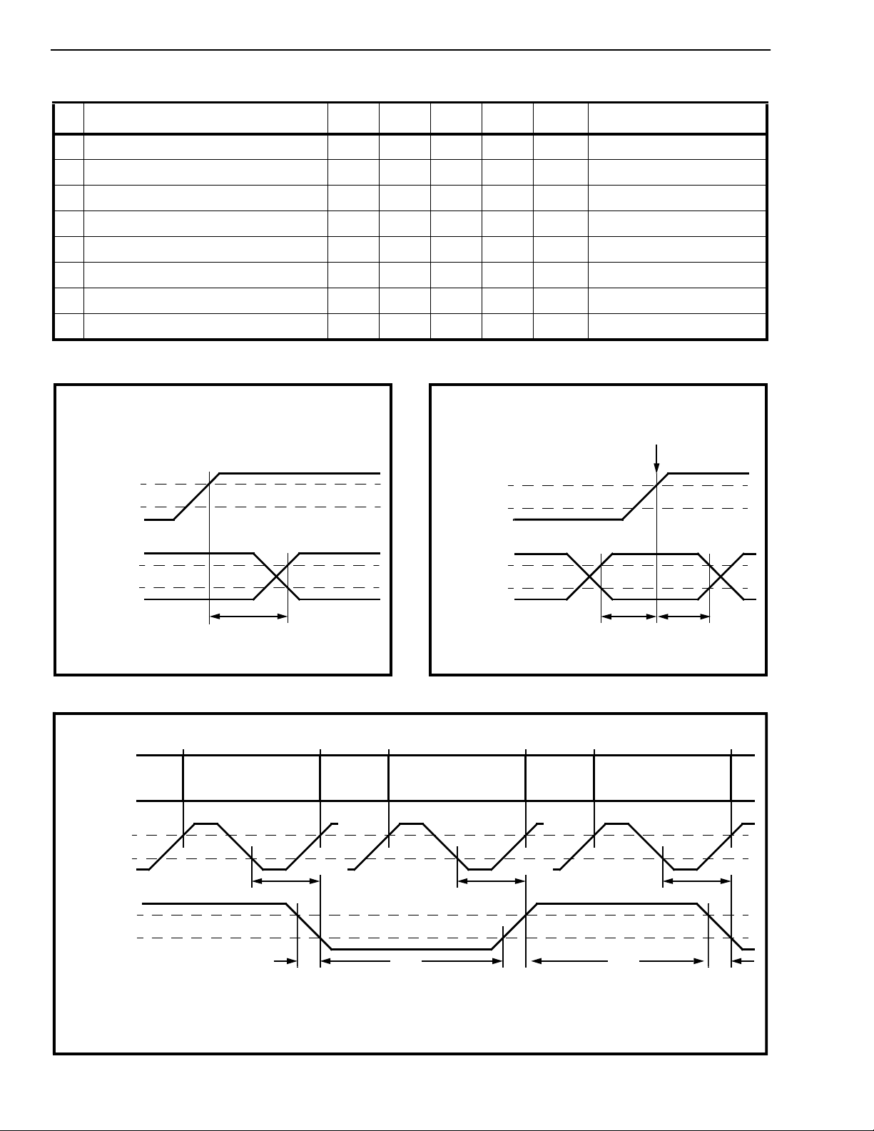
MH89770 Preliminary Information
AC Electrical Characteristics† - XCTL, XSt, & E8Ko (Figure 23, 24, & 25)
Parameters Sym Min Typ
‡
Max Units Test Conditions
1 External Control Delay t
2 External Status Setup Time t
3 External Status Hold Time t
4 8 kHz Output Delay t
5 8 kHz Output Low Width t
6 8 kHz Output High Width t
7 8 kHz Rise Time t
8 8 kHz Fall Time t
† Timing is over recommended temperature & power supply voltage ranges.
‡ Typical figures are at 25°C and are for design aid only; not guarantee d and not subje ct to producti on testing.
ST-BUS Bit Cell Boundary Between
Bit 0 Channel 15 and Bit 7 and Channel 16
C2i
XCtl
2.0V
0.8V
2.4V
0.4V
XCD
XSS
XSH
8OD
8OL
8OH
8R
8F
78 µs
47 µs
C2i
XSt
140 ns
100 ns
400 ns
150 ns
10 ns
10 ns
ST-BUS Bit Cell Bound ary Betwe en
Bit 2 Channel 30 and Bit 1 Channel 30
2.0V
0.8V
2.0V
0.8V
Received
DS1 Bits
E1.5o
E8Ko
Figure 23 - XCTL Timing
Channel 2
Bit 1
V
OH
V
OL
t
8OD
V
OH
V
OL
t
XCD
t
XSS
t
XSH
Figur e 24 - XST Ti mi ng
t
8OL
Channel 17
Bit 2
t
8OD
• • •
t
8F
• • •
t
8R
Chan nel 2
t
t
8OH
Bit 1
8OD
t
8F
4-154
Figure 25 - E8Ko Timing
Page 31
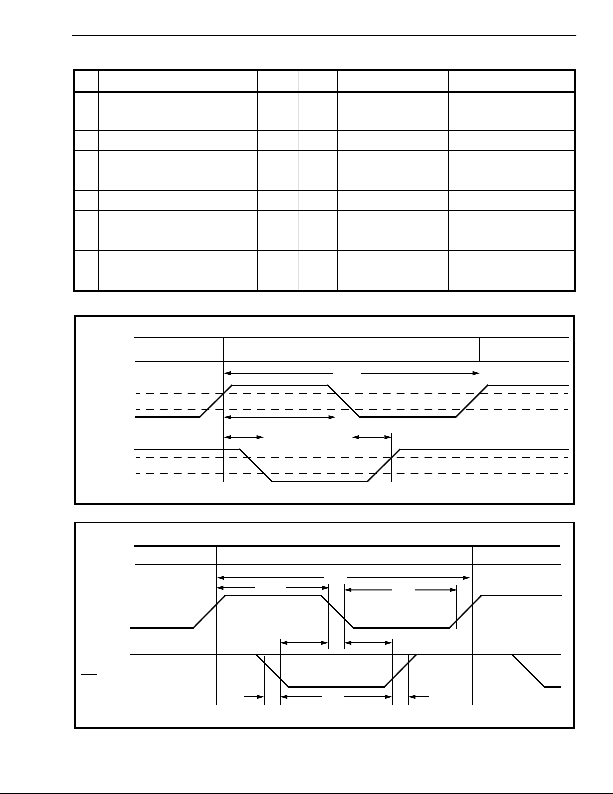
Preliminary Information MH89770
AC Electrical Characteristics† - DS1 Link Timing (Figures 26 and 27)
Characteristics Sym Min Typ
‡
Max Units Test Conditions
1 Transmit Steering Delay t
2 E1.5o Clock Period t
3 E1.5o Clock Widt h High or Low t
4 Re ce ive Data Setup Time t
5 Receive Data Hold Time t
6 Rece ive Data Pulse Widt h t
7 Rece ive Data Fa ll Time t
8 Rece ive Data Rise Time t
9 C1.5i Period t
10 C1.5i Pulse Width High or Low t
† Timing is over recommended operating temperature and power supply voltage ranges.
‡ Typical figures a re at 25°C and are for design aid only: not guaran tee d and not subject to producti on test ing.
Transmitted DS1 Link
Bit Cells
V
C1.5i
IH
V
IL
t
TSD
TSD
PEC
WEC
RDS
RDH
RDW
RDF
RDR
PC1.5
WC1.5
t
WC1.5
50 150 ns 150pF Load
648 ns
324 ns
50 ns
50 ns
324 ns
20 ns
20 ns
500 648 800 ns
250 324 ns
Bit Cell
t
PC1.5
t
TSD
OUTA
or
OUTB
Received DS1 Link
Bit Cells
E1.5o
RxA
or
RxB
V
OH
V
OL
V
OH
V
OL
V
OH
V
OL
Figure 26 - Transmit Timing for DS1 Link
Bit Cell
t
t
WEC
t
RDF
t
RDS
PEC
t
RDW
t
RDH
t
WEC
t
RDR
Figure 27 - Receive Tim ing for DS1 Link
4-155
Page 32
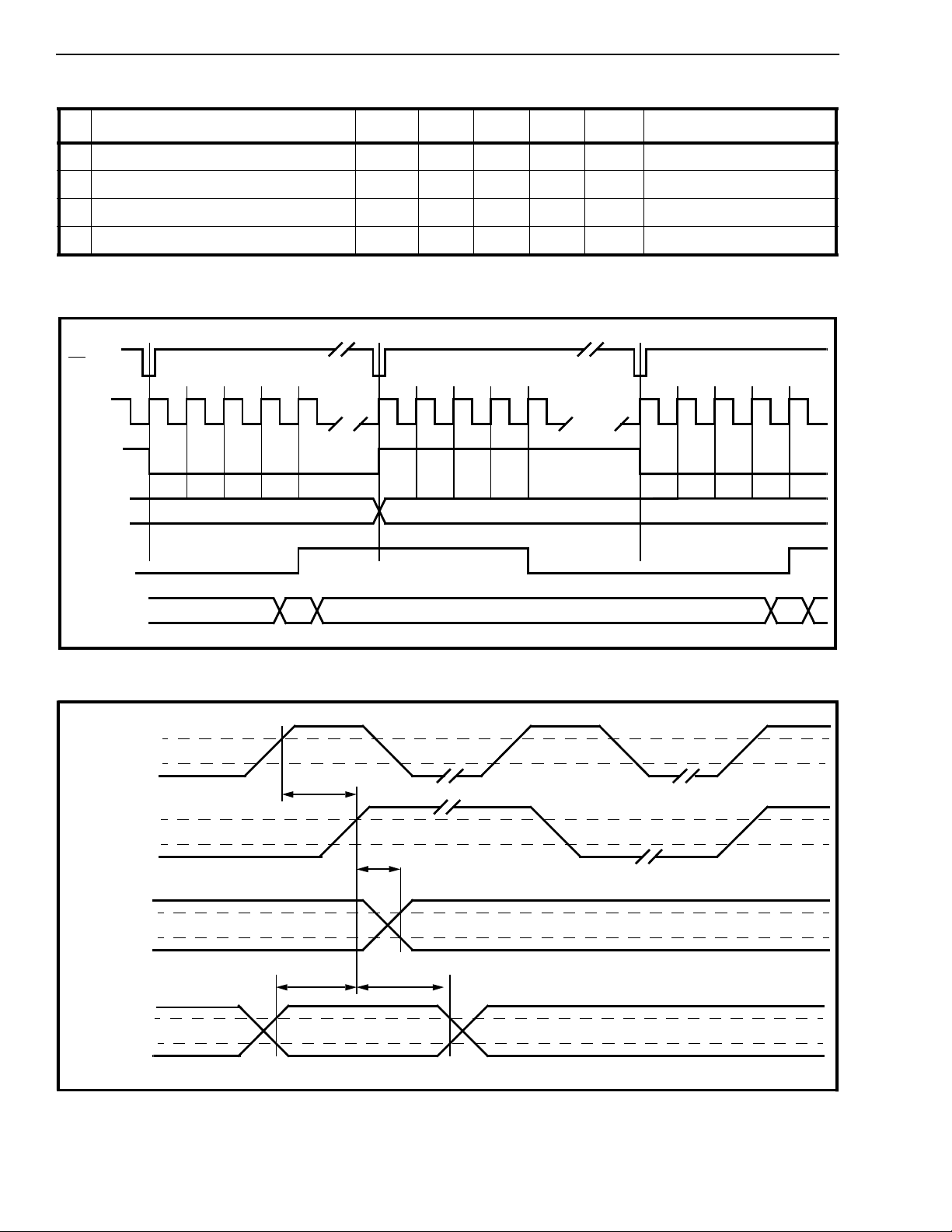
MH89770 Preliminary Information
AC Electrical Characteristics† - DS1 Link Timing (Figure 28 & 29)
Parameters Sym Min Typ‡Max Units Test Cond itions
1 Transmit FDL Setup Time t
2 Transmit FDL Hold Time t
3 Receive FDL Output Delay t
4 Facility Data Link Clock Delay t
† Timing is over recommended temperature & power supply voltage ranges.
‡ Typical figures are at 25°C and are for design aid only; not guarantee d and not subje ct to producti on testing
F0i
C2i
RxFDLClk
RxFDL
TxFDLClk
Frame 12 /24
DLS
DLH
DLOD
FCD
110 ns
70 ns
0 ns 50pF Load
135 ns 50pF Load
Frame 1
.
Frame 2
TxFDL
C2i
TxFDLClk
or
RxFDLClk
RxFDL
TxFDL
Figure 28 - Clock & Frame Alignment for RxFDL and TxFDL
V
IH
V
IL
t
FCD
V
OH
V
OL
V
OH
V
OL
t
DLS
V
IH
V
IL
t
DLOD
t
DLH
4-156
Figure 29 - Facility Data Link Timing
Page 33
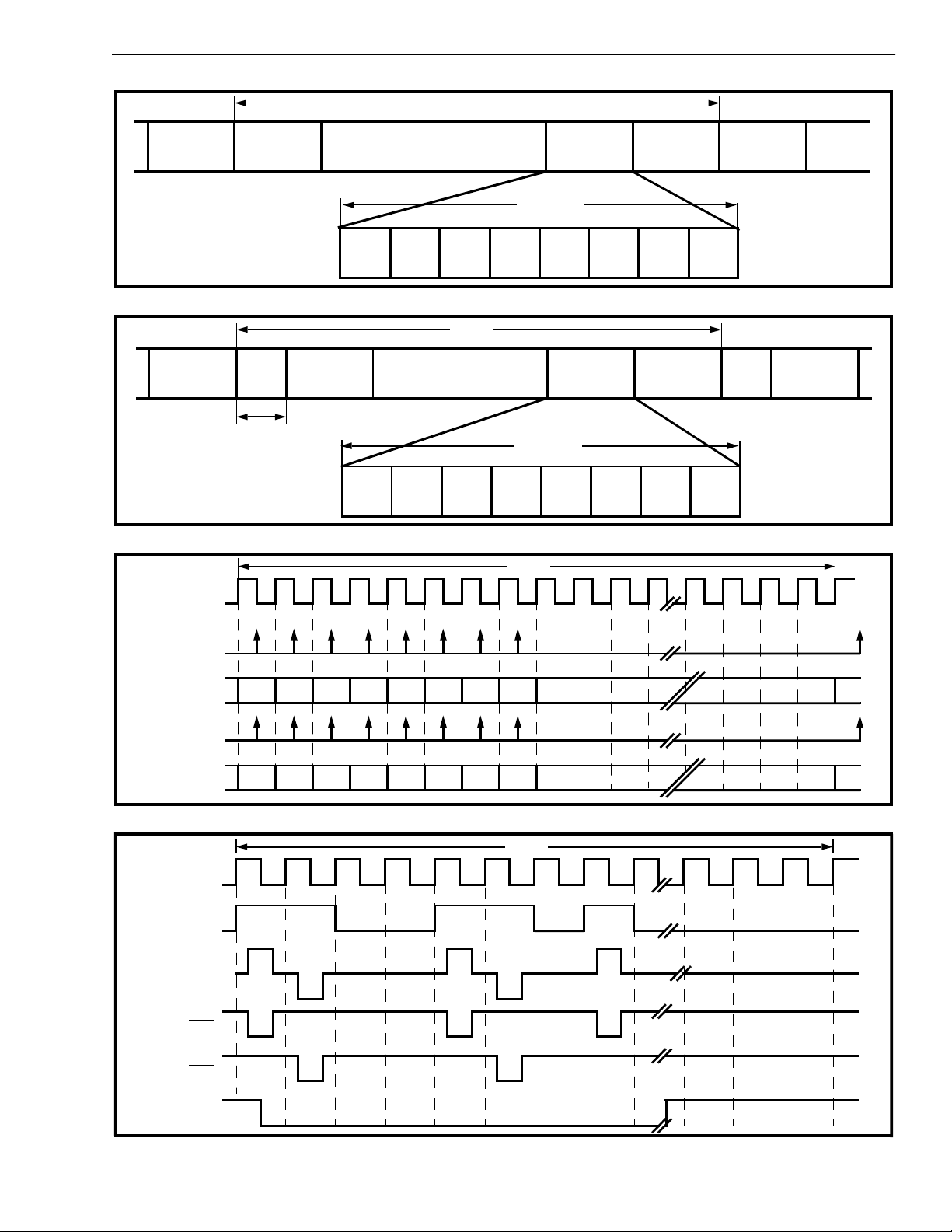
Preliminary Information MH89770
125µs
CHANNEL
31
NB:
Numbering
differs from
Fig 31.
CHANNEL
24
NB:
Numbering
differs from
Fig 30.
CHANNEL
030
Significant
Bit (First)
• • • • • • • •
Most
BIT 7
BIT 6
BIT 5
BIT 4
CHANNEL
(8/2 .048)µs
BIT 3
BIT 2
CHANNEL
31 0
BIT 1
BIT 0
CHANNEL
Least
Significant
Bit (Last)
Figure 30 - Form at of 204 8 kbit/ s ST/BUS Strea ms
125µs
S Bit
(1/1 .544)µs
Significant
Bit (First)
CHANNEL
1
Most
• • • • • •
BIT 1
BIT 2
BIT 3
BIT 4
CHANNEL
(8/1.544)µs
BIT 5
23
BIT 6
CHANNEL
24
BIT 7
BIT 8
S Bit
Least
Significant
Bit (Last)
CHANNEL
Figur e 31 - DS1 Link Fr am e Format
125µs
1
C2i
DSTi
DSTo
CSTi0/CSTi1
CSTo
E1.5i
INT DATA
RxT/RxR
LINE SIGNAL
RxA
765 4321 0
765 43210 7
••••• ••••••
••••• ••••••
7
Figure 32 - Functional ST-BUS Timing
125µs
10111100
RxB
E8Ko
Figure 33 - Functional DS1 Receive Timing
4-157
Page 34
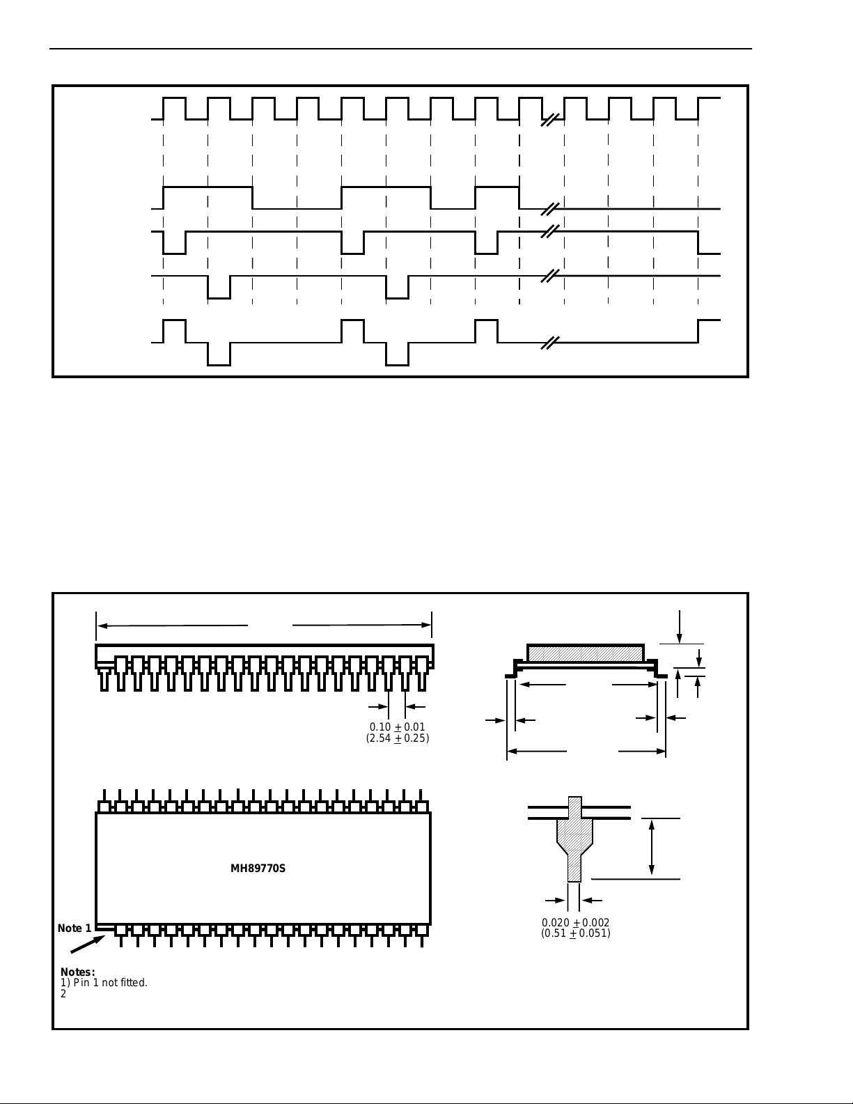
MH89770 Preliminary Information
AAAA
AAAA
AAAA
AAAA
A
A
AAA
AAAA
AAAA
AAAA
AAAA
AAAA
AAAA
AAAA
AAAA
AAAA
AAAA
AAAA
AAAA
AAAA
AAAA
AAAA
AAAA
C1.5i
INT DATA
OUTA
OUTB
AMI LINE
Figure 34 - DS1 Transmit Timing
MH89770S
Note 1
Notes:
1) Pin 1 not fitted.
2) All dimensions are typical and in inches (mm).
3) Not to scale.
Figure 35 - P hys ical Dim en sions for the 40 Pin Dual in L ine S.M.T. Hybr id
4-158
2.0
(50.8)
0.01
0.10 +
(2.54 + 0.2 5 )
0.06
(1.52)
AAA
AAAA
AAAA
AAA
AAAA
AAAA
AAA
AAAA
AAAA
(19.81)
0.020 + 0.002
(0.51 + 0.051)
AAAA
AAAA
AAAA
0.78
0.9
(22.86)
AAAA
AAAA
AAAA
AA
AA
AA
0.3
(7.62)
0.125
(3.18)
0.125
(3.18)
0.06
(1.52)
Page 35
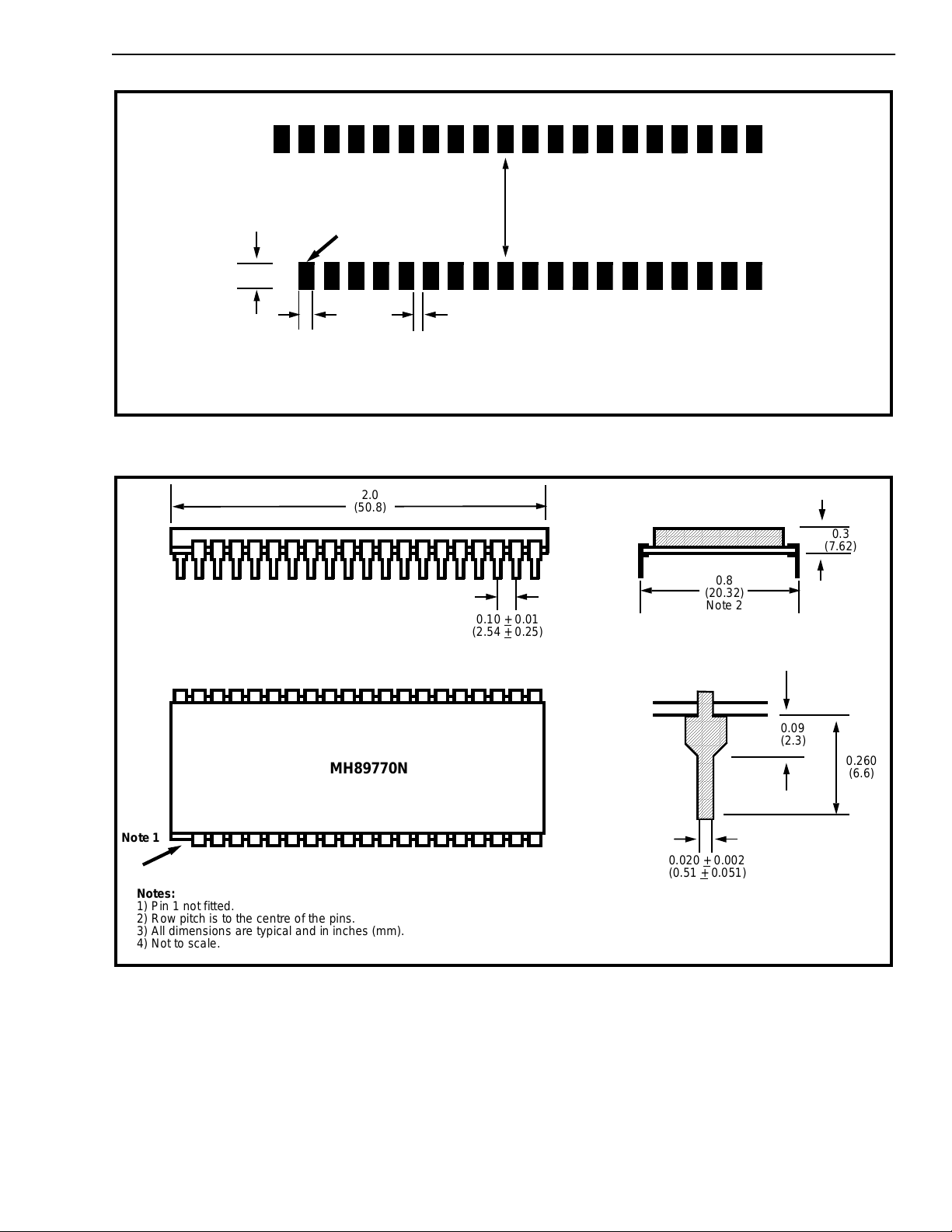
Preliminary Information MH89770
AAAA
AAAA
AAAA
AAAA
A
A
AAA
AAAA
AAAA
AAAA
AAAA
AAAA
AAAA
AAAA
AAAA
AAAA
AAAA
AAAA
AAAA
AAAA
AAAA
AAAA
AAAA
AAAA
AAAA
AAAA
AAAA
AAAA
AAAA
0.760
(19.3)
Pin 2 position
0.090
(2.29)
0.040
(1.02)
0.060
(1.52)
Figure 36 - Recommended Footprint for the 40 Pin Dual in Line S.M.T. Hybrid
2.0
(50.8)
AAA
AAAA
AAAA
AAAA
AAAA
AAA
AAAA
AAAA
(20.32)
AAAA
0.8
AAAA
AA
AA
Note 2
0.10 +
0.01
(2.54 +
0.25)
0.09
(2.3)
MH89770N
0.3
(7.62)
0.260
(6.6)
Note 1
Notes:
1) Pin 1 not fitted.
2) Row pitch is to the centre of the pins.
3) All dimensions are typical and in inches (mm).
4) Not to scale.
Figure 37 - Physical Dimensions for the 40 Pin Dual in Line Hybrid 0.8" Row Pitch
0.020 +
0.002
(0.51 + 0.0 51 )
4-159
Page 36

MH89770 Preliminary Information
Appendix
Control and Status Register Summary
76543210
Debounce
1 Disabled
0 Enabled
TSPZCS
1 Disabled
0 Enabled
B8Z S
1 B8ZS
0 Jammed
Bit
8KHSel
1 Disabled
0 Enabled
XCtI
1 Set High
0 Cleared
ESFYLW
1 Enabled
0 Disabled
Robbed Bit
1 Disabled
0 Enabled
YLALR
1 Enabled
0 Disabled
Master Co ntro l Word 1 (C hann el 15 , CSTi0)
RMLOOP
1 Enabled
0 Disabled
DGLOOP
1 Enabled
0 Disabled
ALL1’s
1 Enabled
0 Disabled
ESF/D4
1 ESF
0 D3/D4
Reframe
Device
Reframes on
High to Low
Transition
SLC-96
1 Enabled
0 Disabled
CRC/MIMIC
See Note 1
Maint.
1 4/12
0 2/4
Master Co ntro l Word 2 (C hann el 31 , CSTi0)
UNUSED - KEEP AT 0
Polarity
1 No Inversion
0 Inversion
Loop
1 Ch. looped
back
0 Normal
Data
1 Enabled
0 Disabled
Per Channel Control Words (All Channels on CSTi0 Except Channels 3, 7, 11, 15, 19, 23, 27 and 31)
UNUSED - KEEP AT 0
A
Txt. Sig. Bit
B
Txt. Sig. Bit
C
Txt. Sig. Bit
D
Txt. Sig. Bit
Per Channel Control Words (All Channels on CSTi1 Except Channels 3, 7 , 11, 15, 19, 23, 27 & 31)
YLAIR
1 Detected
0 Normal
MIMIC
Detected
0Not
Detected
ERR
F
T
Count
Error
ESFYLW
1 Detected
0Not
Detected
MFSYNC
1 Not Detected
0 Detected
BPV
Bipolar
Violation
count
SLIP
Changes
State
when Slip
Performed
SYN
1 Out-of-Sync.
0 In-Sync
Master Status Word 1 (Channel 15, CSTo)
BlAlm
1 Detected
0 Not Detected
Per Channel Status Word (All Channels on CSTo Except Channe ls 3, 7, 11, 15, 19, 23, 27, 31)
Note 1: In ESF m o de :
In D3/D4 mode:
1: CRC calc. ignored during Sync.
0: CRC checked for Sync.
1: Sync. t o first correc t S-bit patt ern .
0: Will no t Sync. if M im ic d ete c ted .
FrCnt
Frame
Count
XSt
1 Xst High
0 Xst Low
BIPOLAR VIOLATION COUNT CRC-ERROR COUNT
Master Status Word 2 (Channel 31, CSTo)
CHANNEL COUNT BIT COUNT
Phase Stat us Word (Chan nel 3, CSTo)
UNUSED
A
Rec’d. Sig. BitBRec’d. Sig. BitCRec’d. Sig. BitDRec’d. Sig. Bit
4-160
 Loading...