

Page 1
MH88630
Central Office Interface (LS/GS)
Preliminary Information
Features
• Transformerless 2-4 W ire conversion
• Line state dete ction out put s:
- forward current
- reverse current
- ring ground
- tip ground
- ringing voltag e
• Programmable audio transmit and receive gain
• Loop start o r ground start termin ation
• Selectable 600Ω or AT&T comp romis e bala nce
network
Applications
• PBX Interface to Central Office
• Channel bank
• Intercom
• Key system
ISSUE 7 April 1995
Ordering Information
MH88630 40-Pin DIL Package
0°C to 70°C
Description
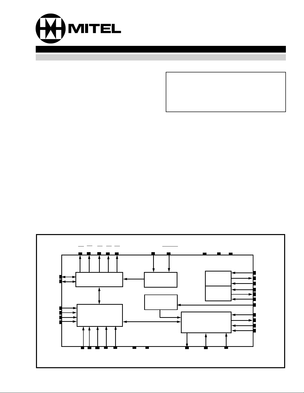
The Mitel MH88630 Central Office Trunk Interface
circuit provides a complete audio and signalling link
between an audio switching equipment and a central
office. The loop seize circuitry is controlled by an
external input to provide either a loop start or ground
start termination. The device is fabricated using thick
film hybrid technology to achieve high density circuit
design.
R
VTR+
VTR-
RXINRXIN+
VCC-
Relay
Driver 1
Relay
Driver 2
AGND
RC1
RD1
RGND
CD
RD2
RC2
NETBAL
GSX
VX
VR
GSR
FC
RG
T
Signal Detection
Termination
QB QE XA XB XC VDD VEE RXOUT TXIN+ TXIN-
Circuitry
Active
RCRV
LPGNDTG
RINGND
Ring
Ground
Network
Balance
VCC+
Audio Sec t ion
Circuitry
(2 - 4 Wire)
Figure 1 - Functional Block Diagram
2-215
Page 2
MH88630 Preliminary Information
IC
IC
IC
LPGND
RINGND
VTR+
QE
QB
VTR-
XA
XB
XC
RGND
RC1
RD1
CD
RD2
RC2
1
2
T
3
R
4
5
6
7
8
9
10
11
12
13
14
15
16
17
18
19
20
40
39
38
37
36
35
34
33
32
31
30
29
28
27
26
25
24
23
22
21
RG
FC
RV
RC
TG
VDD
VEE
AGND
RXINRXIN+
NETBAL
VX
GSX
TXIN+
TXINVCCVCC+
RXOUT
GSR
VR
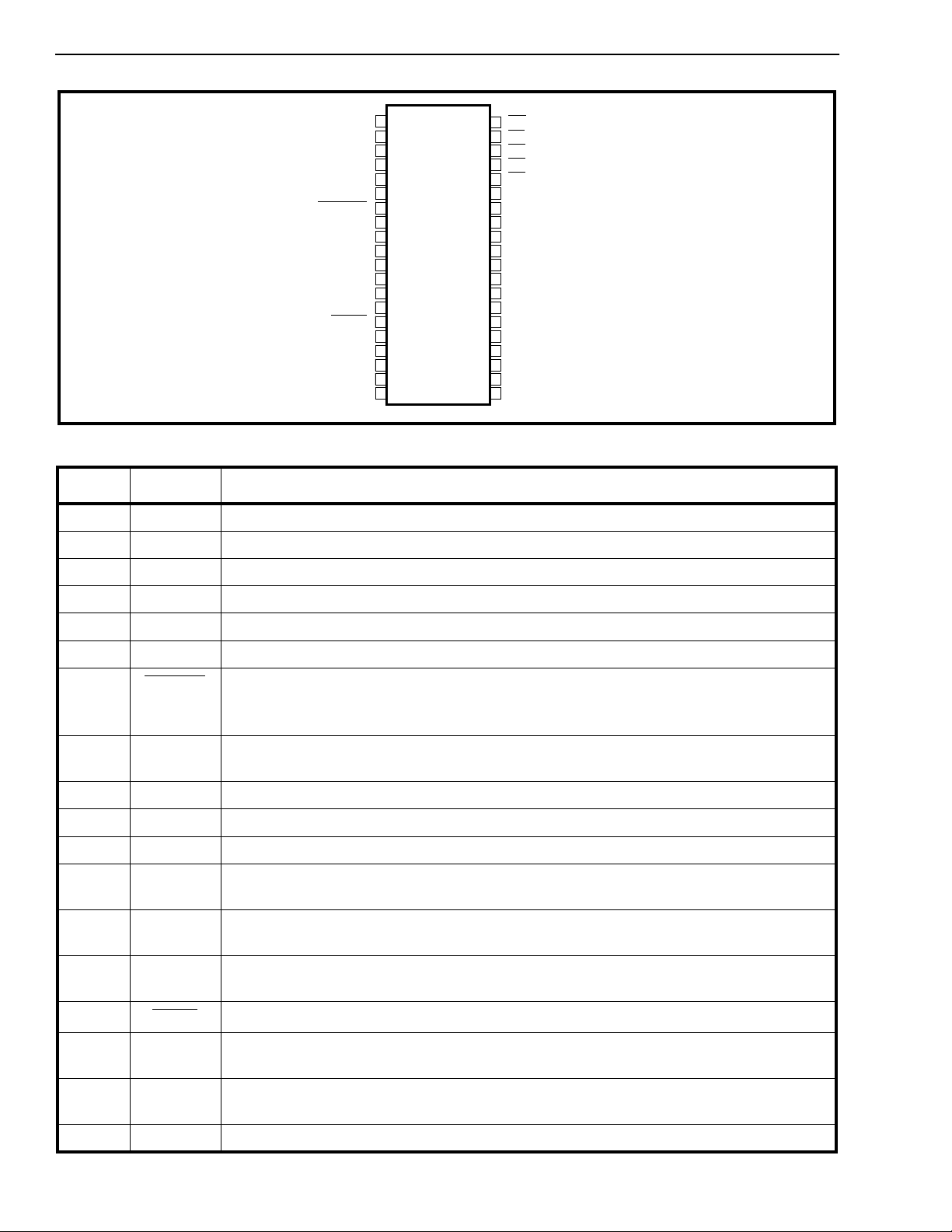
Figure 2 - Pin Connections
Pin Description
Pin # Name Description
1ICInternal Connection. Pin cut short. Leave open circuit .
2TTip (Input). Normally connects to the “Tip” lead of the C.O.
3RRing (Input ). Normally connects to the “Ring” lead of the C.O.
4ICInternal Connection. Leave open circuit.
5ICInternal Connection. Leave open circuit.
6 LPGND Loop Ground is the system ground reference with respect to -48 volts.
7 RINGND
Ring Ground (Input). For Ground Start Trunk only, a logic low input will enable the trunk
circuit to ground the Ring lead through a low resistance (390Ω). This is a signal to the
C.O. that the interface is seizi ng the li ne.
8 VTR+ Connects to the coll ector of an external transist or (Q1) and TX IN - (pin 26) via an
external capacitor.
9 QE Connects to the emitter of an external tran sistor (Q1).
10 QB Connects to the base of an external transistor (Q1).
11 VTR- Connects to the TXIN+ (pin 27), via an external ca pacito r (C1).
12 XA External relay contact (K1) connection from VTR+ (pin 8), activated by loop seize control
input (RC1).
13 XB External relay contact (K1) connection from XC (pin 14), activated by loop seize control
input (RC1).
14 XC E xternal relay contact (K1 ) connection from XB (pin 13), activat ed by loop seize control
input (RC1).
15 RGND
Relay Gro und.
16 RC1 Relay Contr ol 1 (Input). A logic high will activate the relay (K1) to provide loop seize
across Tip and Ring.
17 RD1 Relay Driver 1 (Output): Open collector sinks current when RC1 is high. Diode clamp
protected.
18 CD Clamping Diode: Normally connects to the positive supply voltage.
2-216
Page 3
Preliminary Information MH88630
Pin Description (Contin ue d)
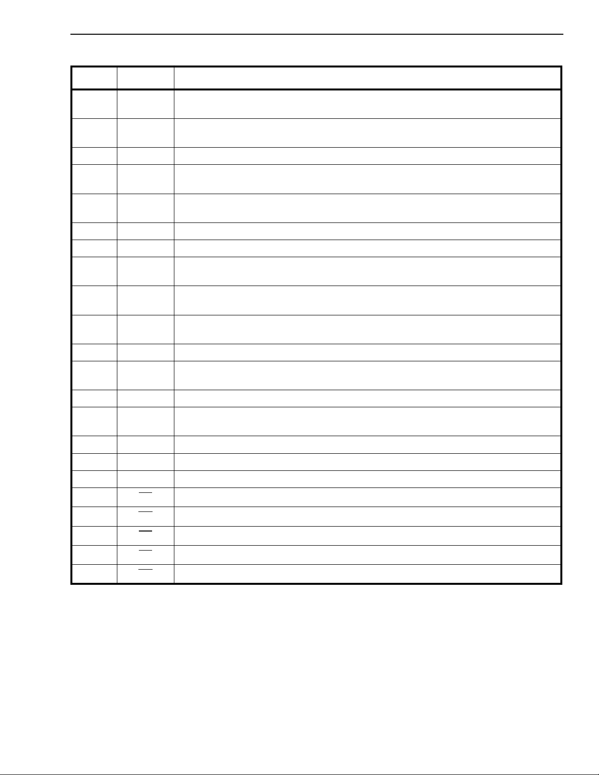
Pin # Name Description
19 RD2 Relay Driver 2 (Output): Open collector sinks current when RC2 is high. Diode clamp
protected.
20 RC2 Relay Contr ol 2 (Input): A logic high will activate the relay (K2) to provide proper
biasing to the tip and ring. This input control is used for Ground Start Trunk only.
21 VR Audio Receive (I nput). The 4-wire audio signal input to the interface.
22 GSR Gain Setting Receive (Input). Normally used to set the receive gain with an external
resistor connected to RXOUT (pin 23).
23 RXOUT Audio receive signal (output) to the RXIN- (pin 32), via an external decoupling capacitor
(C3).
24 VCC+ Positive analog P ow er Supp ly Voltage (+12V).
25 VCC- Negative analog Power Supply Voltage (-12V).
26 TXIN- Transmit (Input). Different audio signal from VTR+ (pin 8), via an external capacit or
(C4).
27 TXIN+ Transmit (Input). Different audio signal from VTR- (pin 11), via an external decoupling
capacitor (C1).
28 GSX Gain Setting Transmit (Input). Normall y used to set the transmit gain wit h an external
resistor connected to VX (pin 29).
29 VX Audio Transmit (Output). The 4-wire audio signal outp ut from the interf ac e.
30 NETBAL Network Balance (Input). When there is no connection (open), the network is balanced
at 600Ω. When this pin is grounded, the network is balanced at AT&T compromise.
31 RXIN+ Differential Receive (Input). Connects to analog ground via an external capacitor (C2).
32 RXIN- Differential Receive (Input). Connects to RXOUT (pin 23) via an external capacitor
(C3).
33 AGND Analog Gro und .
34 VEE Negative Power Supply (-5V).
35 V DD Positive Power Supply (+5V).
36 TG
37 RC
38 RV Ringing Voltage Detect (Output). Active low.
39 FC Forward Loop Current Detect (Output). Active low
40 RG
Tip Lead Ground Detect (Output). Active low.
Reverse Loop current Detect (Output). A ctive low.
Ring Lead Ground Detect (Outp ut). Active low.
2-217
Page 4

MH88630 Preliminary Information
Functional Description
The MH88630 is a Central Office Loop Start and/or
Ground Start Analog Trunk interface circuit providing
a complete audio and signalling link to the Central
Office.
The trunk interface circuit performs transformerless
2 to 4 wire conversion, between the 2-wire telephone
loop and the 4-wire transmit and receive pairs of a
voice switching system. The 4-wire connection can
be interfaced to a filter/codec, such as the MT896X,
for use in a digital voice switched system.
Voiceband analog signals, coming from the C.O.,
applied differentially across Tip and Ring, pass
through a bridge rectifier and appear at VTR+ and
VTR- where they are actively terminated. Refer to
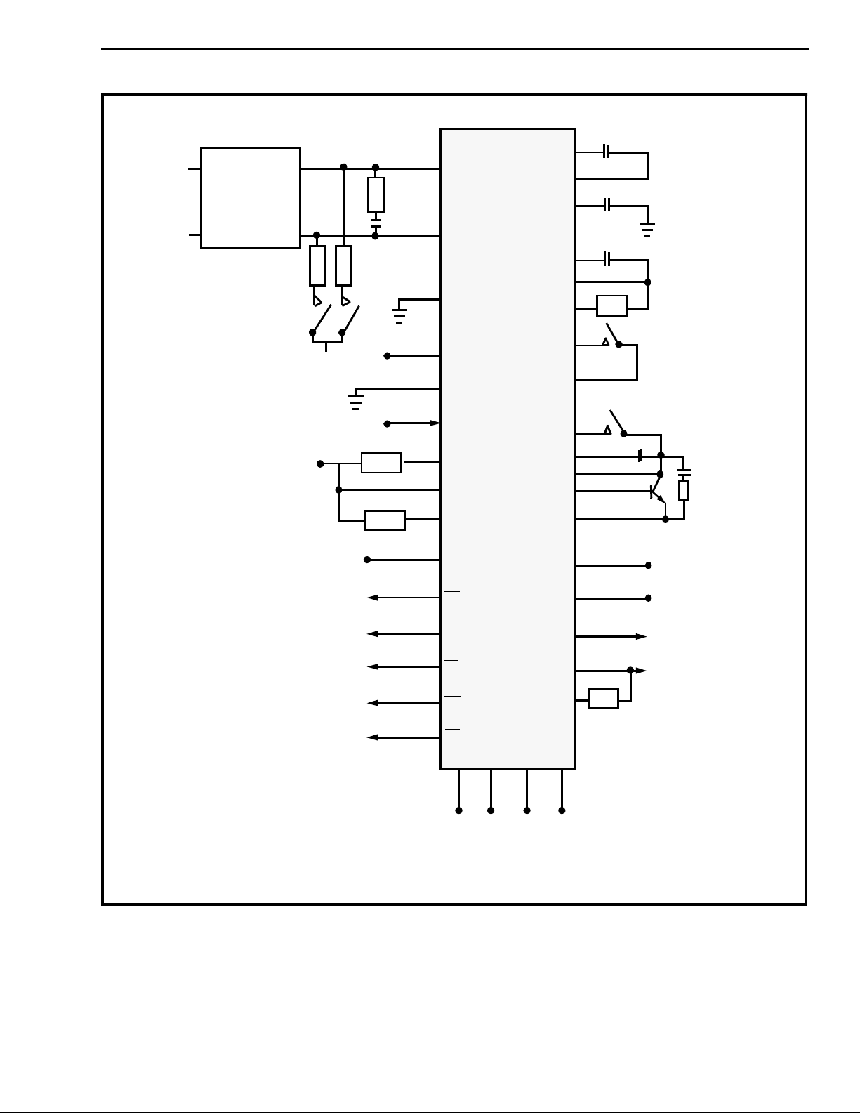
Fig 3 - Application Circuit. External capacitors C1
and C4 couple the incoming signals into the
balance d in put of th e rec eiv e au dio cir cuit vi a TX IN +
and TXIN-. The receive gain is adjusted by feedback
resistor R4. For best performance R4 should be
physically located as close as possible to the GSX
pin. The gain adjusted receive signal appears at the
Vx output pin.
Relay K1 is the loop seize relay which applies active
line termination and also provides biasing of the
current modulator circuit. Activating and deactivating
K1 provides dial pulsing. Q1 is the current modulator
output transistor, referred to as the loop drive
transistor.
Outgoing analog signal from the system are provided
to the interface at the VR input where they enter an
amplifier section with the gain controlled by the
selection of the Tx gain feedback resistor R3. For
best performance, R3 should be physically located
as close as possible to the GSR pin. The output of
the amplifier, RXOUT is coupled to RXIN- the current
modulator circuitry, via C3. The balanced input to the
current modulator is completed with the connection
of C2 from RXIN+ to ground. Transmission to the
C.O. is accomplished by modulating the loop with the
outgoing analog signals. To ensure that the
transmitted signals are not coupled to the receive
circuitry, transhybrid loss is maximised. The
impedance matching, performed by the balanced
network reduces power loss and signal reflections.
The network balance input, NETBAL, of the
interface’s 2-wire to 4-wire converter circuitry
provides selection of a 600Ω balance, used when
feeding channel banks or when performing external
tests on the trunk circuit, or the AT&T compromise.
With the NETBAL input pin left the interface is
balanced to match to 600Ω. If the NETBAL in put pin
is grounded, the interface is balanced against the
AT&T compromise network consisting of 350Ω plus
1kΩ shunted by a 0.21µF capacitor. This is intended
for typical N o rth American C .O . connection s .
The Tip and Ring also enter the balanced input of the
signal detection circuitry which provides the
signalling st atus outputs TG
For Ground Start signalling, relay K2 and resistor R1
and R2, are required. Activation of K2 is controlled
by the relay c ontrol logic input signal RC2. In the idle
state, K2 is closed connect ing the -48Vdc supply to
Tip and Ring through biasing resistors R1 and R2.
Upon detection of TG or RG, the system them pulls
RC1+ low closing K1, then pulls RC2 low which
opens K2 to remove the -48V volts supply from Tip
and Ring.
In the Ground Start signalling environment, initiating
a call to the C.O. is preformed by the following
sequence of events. The system provides a logic low
on the ring ground input pin of the interface. This
activates the circuit which grounds the ring lead
through a current limiting resistance. The C.O.
recognises the ground condition and connects th e tip
lead to ground. The interface senses this condition
and the tip lead ground detect output switches to a
logic low. The system then applies active line
termination by closing K1 using RC1 and opens K2
using RC2. A call from the C.O. can be performed
similarly. The C.O. can signal to the interface by
pulling either Tip or Ring to ground potential, or by
applying ringing voltage to the ring lead.
Signal Detection Circuitry
The signal detection circuit provides the signalling
status output. The system, controlling the interface,
monitors these active low logic outputs. RV is the
Ringing Voltage detect output. When the C.O.
applies ringing voltage to the termination, the trunk
interface provides a 50ms debounced outputs at RV
during the ringing burst period. This output will
remain low for approximately 50ms after the C.O.
removes the ringing voltage. Ringing voltage above
40 VRMS at 20 Hz will be detected.
TG is the Tip lead Ground det ect output and RG is
the Ring lead Ground detect output. The TG
outputs provide a means of determining call
origination or other handshaking functions. The high
, RC, RV, FC and RG.
and RG
2-218
Page 5

Preliminary Information MH88630
impedance detection circuitry of the interface will
detect both Tip and Ground and Ring Ground
voltages above approximately -15.3V of true ground.
is the Reverse loop current detect output and FC
RC
if the Forward loop Current detect output. The RC
and FC outputs of the interface are used to
dete rm in e th e p ola rit y o f t he Ti p a nd R ing pair wh ich
the C.O. uses for signalling during the active (off-hook)
state of the interf ace. When the loop is closed by the
interface, the trunk is in the normal or unreversed
state. Some C.O.’s may reverse the polarity of Tip and
Ring, to indicate the talking state. The interface will
detect this condition and RC
External Circuitry Requirements
The loop seize circuit is complet ed wit h the addition
of external com ponents Q1, C5, R5 and K1.
K1, a DPST reed relay, is activated by relay control
signal RC1. When the loop seizure is required, K1 is
closed and the interface applies active termination
across Tip and Ring. The relay should have a 0.5
amp contact capability and 12 VDC operation with a
typical 500Ω coil resistance. To prevent back EMF
from damaging the relay drive transistor, (caused by
the collapsing field of the inductive coil of the relay) a
snubbing diode is provided on the hybrid and
therefore not required externally. C5 and R5 provide
relay contact noise filtering and transient noise
suppression necessary for clamping inductive spikes
created when the loop is closed during line seizure
or dial pulsing.
Q1 provides current drive for the active termination,
controlling the loop current flow of the current
modulator circuitry. Selection of a suitable transistor
for Q1 is made based on worst case conditions
which include fault conditions. A 350 volt, or higher,
rating for Q1 is necessary to meet high voltage
requirements. The Tip and Ring input protection
varistors limit any high voltage spikes to
approximately 300 volts. Under worst case
conditions Q1 must be able to handle close to
100mA of collector current and dissipate two watts
continuously. During pulse dialling, current spikes
are generated due to the inductive nature of the loop.
A 0.5 amp continuous connector current rating is
therefore recommended to provide a safe margin.
will output a low level.
is provided on the hybrid. R1 and R2 provide the
-48V biasing the signalling (on-hook) state.
R6 and C6 constitute the Dummy Ringer required for
the LS/GS trunk. These component s are also part of
the 600Ω input impedance.
A protection circuit on the Tip and Ring inputs may
be required depending upon the trunk interface
application. For maximum protection it is
recommended to place fuses in series with the Tip
and Ring inputs of the interface, following by metal
oxide varistors from Tip and Ground, Ring to Ground
and Tip to Ring.
Components List (for Figure 3)
R1*, R2 = 30.9kΩ, ± 1%, ¼ W
= Receive Gain Adjust Resistor
= 523.2 E3 x Gain VTR/VR
Typi cal Value = 505kΩ , ±1 %, ¼ W
R3 = Transmit Gain Adjust Resistor
= 301.5 E3 x Gain VX/VTR-100 E3
Typ ical V alue = 200k Ω, ± 1%, ¼ W
R5 = 510Ω, ± 5%, ¼ W
R6 = 10kΩ, ± 5%, ¼ W
C1, C2, C3 , C 4 = 0.22µF, ± 10%, 200V
C5 = 0.1µF, ± 5%, 250V
C6 = 1.0µF, ± 5%, 250V
Q = 2N5657, NPN 350V, 0.5A, 20W
K1, K2 = 2A Re ed r e lay, E/M 12V
2 Form C Dip
*Note: required for Ground Start applications, not
required for Loop Start applications.
K2, R1 and R2 are required only for Ground Start
applications. K2 is the same type of relay as K1 and
is activated by RC2. Once again the snubbing diode
2-219
Page 6
MH88630 Preliminary Information
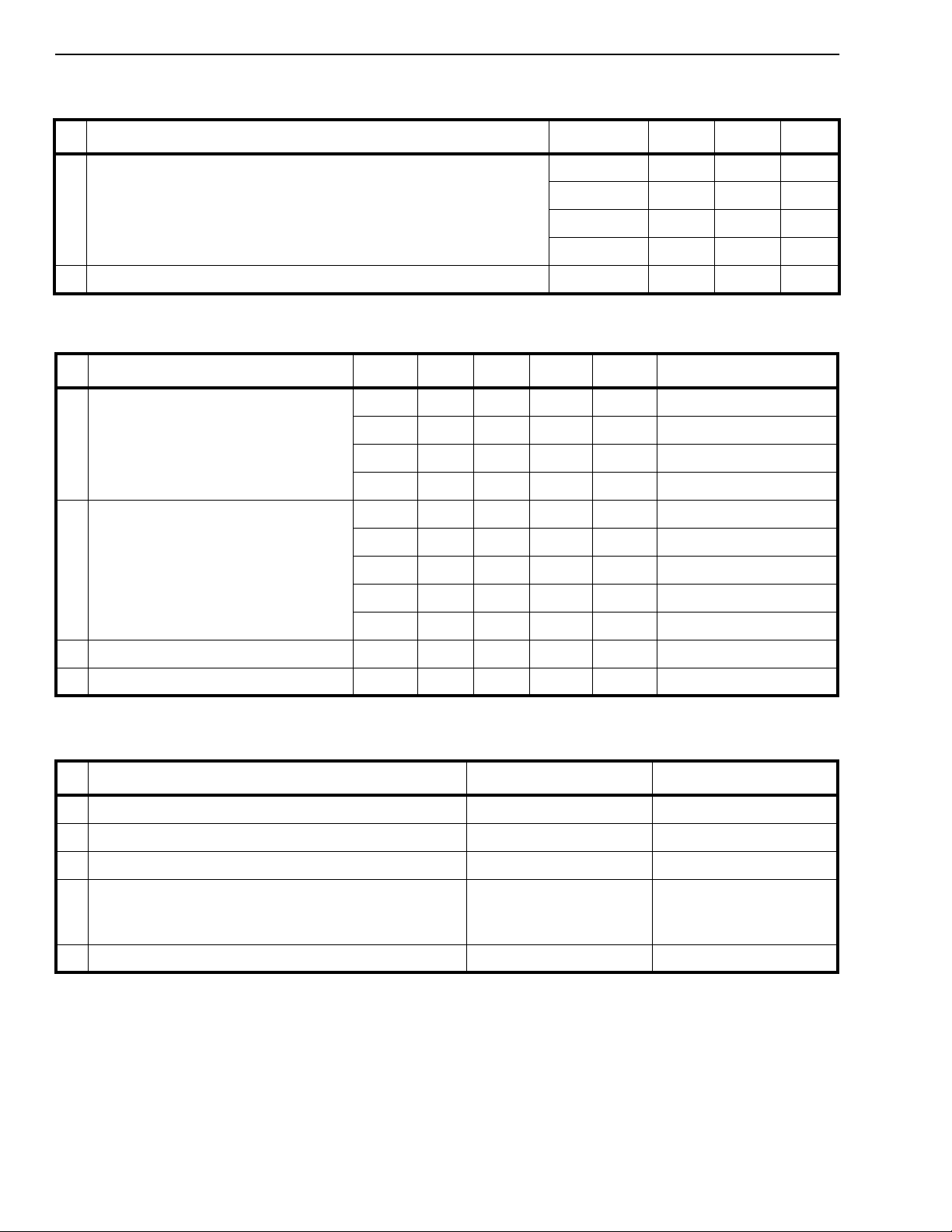
Absolute Maximum Ratings* - Voltages are with respect to AGND.
Parameters Sym Mi n. M ax Units
1 DC Supply Voltages V
2 Storage Temperature T
-GNDA -0.3 +6.0 V
DD
V
-GNDA -6.0 + 0.3 V
EE
V
-GNDA +18.0 V
CC+
V
-GNDA -18.0 V
CC-
STG
* Exceeding these values may cause damage. Functional operation under these conditions is not implied.
Recommended Operating Conditions
Parameters Sym Min. Typ
1 Operating Supply Voltage V
V
V
V
DD
EE
CC+
CC-
2 Operating Curre nt V
I
DD
I
EE
I
CC+
I
CC-
3 Power Consumption P
4 Operating Temperature T
‡ Typical figures are at 25°C and are for design aid only: not guaran teed and no t subject to producti on testing .
OP
4.75 5.0 5.25 V
-5.25 -5.0 -4.75 V
11.4 12.0 12.6 V
-11.4 12.0 -12.6 V
Bat
C
070°C
‡
Max Units Comments
-48 V
7.0 mA RIN GND High
-7.0 mA
8.0 mA
-8.0 mA
265 mW
-55 +125 °C
Control Inputs State Table
Parameter Active Idle
1 RC1 Logic High Logic Low
2 RC2 Logic High Logic Low
3 RINGND Logic Low Logic High
4 NETBAL
AT&T compromise network
(350Ω + 1kΩ // 0.21µF) AGND
6000Ω network Open (no connection)
2-220
Page 7

Preliminary Information MH88630
AC Electrical Characteristics†
Characteristics Sym Min Typ‡Max Units Test Conditions
1 Ringing Voltage
VR 40 90 130 V
rms
2 Ringing Frequency 20 Hz Ringing Type A, RS-464
3 Operating Loop Current
4 Off-Hook DC Resistance
5 Operating Loop Resistan ce
IL 18 70 m A
RT 300 Ω @18mA
RL 2300 Ω @18mA
6 On-Hook Leakage Current 3 µA RINGND = 5.0Vdc
7 Ring Ground Sink Current
IRG 100 mA -48VDC with 200Ω in
series on Ring lead
8 Tip and Ring AC Impedance 600 Ω with 10kΩ + 1.0µF
inparallel with Tip and
Ring
9 Longitudinal Balance
metallic to longit udina l
longitudinal to metallic
10 Return Loss
Trunk to Lin e
60
40
58
53
20
26
30
dB
dB
dB
dB
dB
dB
dB
200-1000Hz
1000-4000Hz
200-1020Hz
1020-3020Hz
200-500Hz
500-1000Hz
1000-3400Hz
11 Transhybrid Loss (single
frequency) into 600Ω
12 Transhybrid Loss (single
frequency) into AT&T
THL 16 18.5
34
30
THL 16
18
18
21
dB
dB
dB
200Hz
1000Hz
3000Hz
dBdB200-1000Hz
1000-4000Hz
Compromi se
13 Frequency response (Output
relative to 1kHz,
VTR/VR and VX/VTR)
-0.15
-0.10
-0.10
-0.15
0.05
0.05
0.05
0.05
dB
dB
dB
dB
200Hz
300Hz
3000Hz
3400Hz
See Note 1
14 Idle Channel Noise 8 13
dBrncO
C-Message
15 Power Supply rejection ratio PSRR 40 dB
16 Analog signal overload level
(adjustable gain)
† AC Electrical Characteristics are over recommended operating conditions unless otherwise stated.
‡ Typ ical figures are at 25°C and are for desi gn aid only: not guaran teed and not subje ct to producti on testing.
Note 1: Input 0dBm at VTR, or input 0.775Vrms at VR. TR-600Ω termination
6 dBm 1kHz, 0dBm= 0. 775Vrms
into 600Ω.
2-221
Page 8
MH88630 Preliminary Information
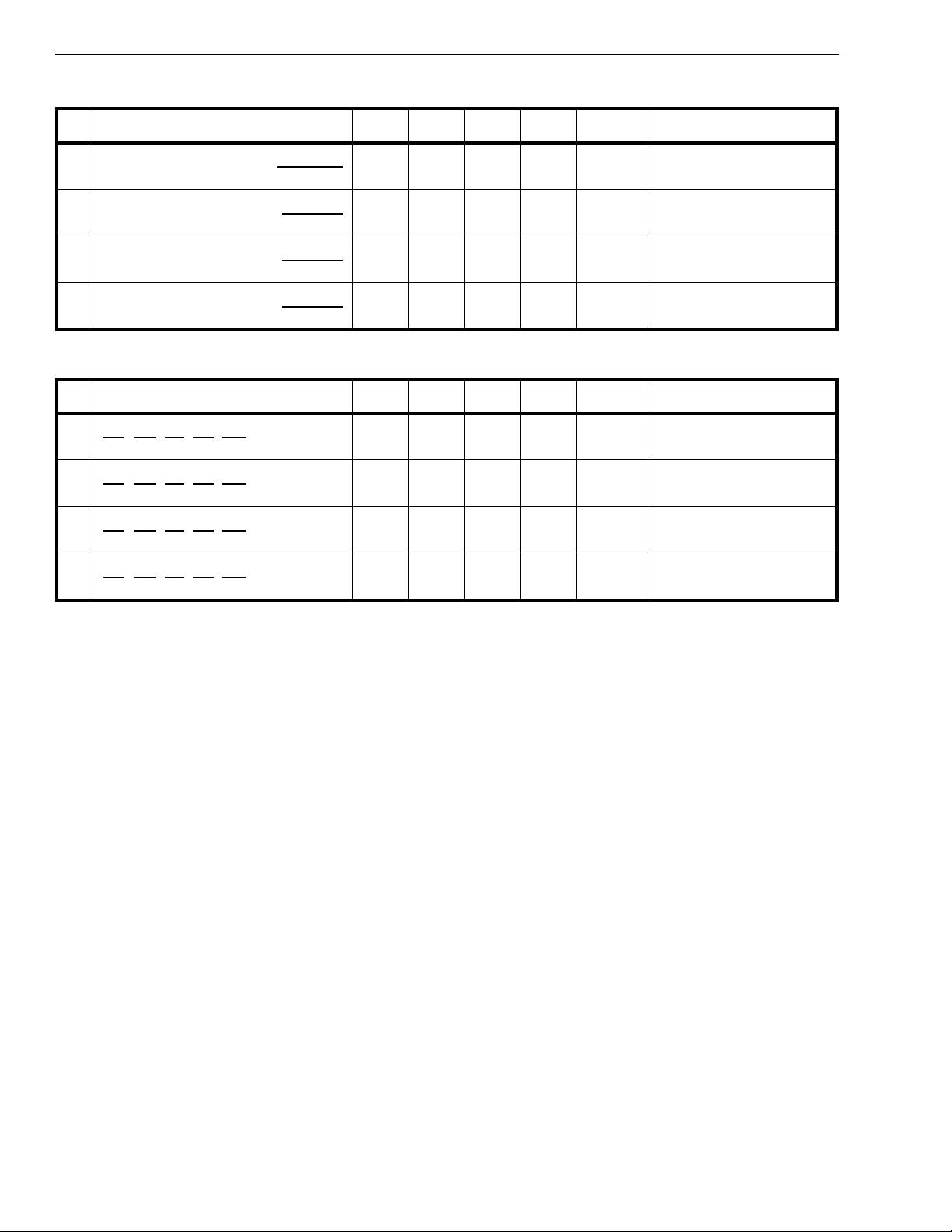
DC Electrical Characteristics - Control Inputs
Characteristics Sym Min Typ Max Units Test Conditions
1 Input High Voltage RC1, RC2
RINGND
2 Input High Current RC1, RC2
RINGND
3 Input Low Voltage RC1, RC2
RINGND
4 Input Low Current RC1, RC2
RINGND
V
IH
I
IH
V
I
IL
2.7
4.5
2.5
5.0
-100
IL
0.7 V
1.0
1.1
DC Electrical Characteristics*
Characteristics Sym Min Typ Max Units Test Conditions
1 Output High Voltage
, RC, RV, FC, RG) 4.75 V No Load on output
(TG
2 Output High Current
, RC, RV, FC, RG)0.17mAV
(TG
3 Output Low Voltage
, RC, RV, FC, RG) -0.3 V No Load on output
(TG
4 Output Low S ink Current
, RC, RV, FC, RG) -0.40 mA VOL= -0.4Vdc
(TG
* DC Electrical Characteristics are over recommended operating conditions unless otherwise stated.
V
V
mA
µA
µA
mA
= -2.7Vdc
OH
2-222
Page 9
Preliminary Information MH88630
MH88630
C1
VTR-
RXIN-
GSR
XB
XC
XA
TXINVTR+
QB
QE
31
32
22
9
11
27
23
13
14
12
26
8
10
C2
C3
R3
K1A
K1B
C4
Q1
C5
R5
TIP
RING
LIGHTNING
PROTECTION
DUMMY RINGER
R1
K2A
-48V BATTERY
+12V
R6
C6
R2
K2B
-48V RETURN
K2
K1
2
3
33
15
20
19
18
17
T
TXIN+
RXIN+
R
RXOUT
AGND
6
LPGND
RGND
RC2
RD2
CD
RD1
16
RC1
37
RC
38
RV
39
FC
40
RG
36
TG
V
V
DD
35 34
+5V -5V +12V -12V
EE
NETBAL
RINGND
V
CC+
24
VR
GSX
V
25
VX
CC-
Figure 3 - Application Circuit
30
7
21
29
28
R4
2-223
Page 10
MH88630 Preliminary Information
AAAA
AAAA
AAAA
AAAA
AAAA
AAAA
AAAA
AAAA
AAAA
AAAA
AAAA
AAAA
AAAA
AAAA
AAAA
AAAA
AAAA
AAAA
AAAA
AAAA
AAAA
AAAA
AAAA
AAAA
AAAA
AAAA
AAAA
AAAA
AAAA
AAAA
AAAA
AAAA
AAAA
AAAA
AAAA
AAAA
AAAA
AAAA
2
(50.8)
2
(50.8)
0.015
(0.381)
Components
0.04
(1.02)
0.030 ± 0.015
(1.91 ± 0.381)
0.16 ± 0.05
(4.06 ± 1.27)
0.01
(2.54)
0.18 ± 0.015
(4.57 ± 0.381)
Pin 1
Pin 2
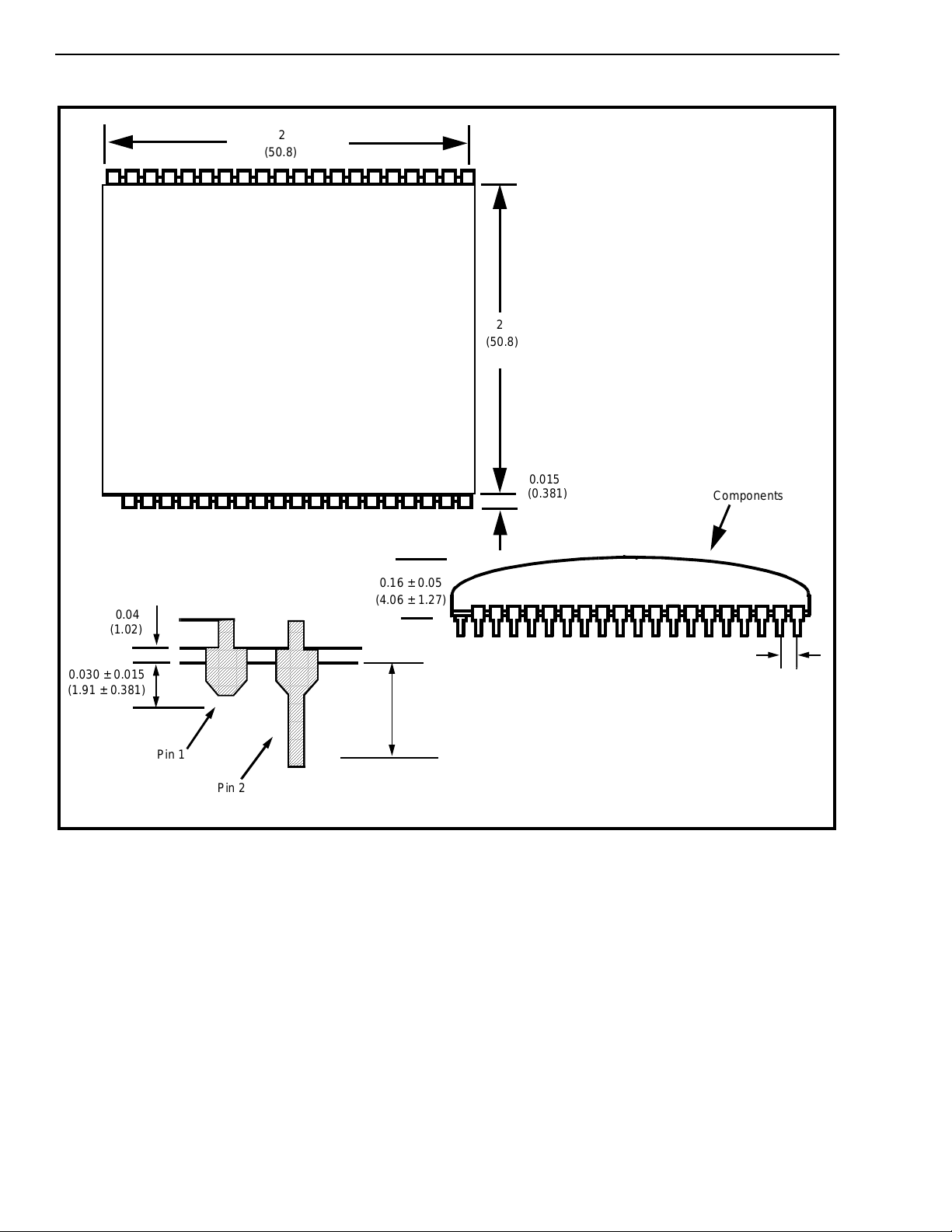
Figure 4 - Physical Dimensions of 40 Pin Dual in Line Hybrid Package
2-224
 Loading...