

Page 1
MH88628
Central Office SLIC
Preliminary Information
Features
• Programm able gain, ne twork bal anc e and
impedance
• Transformerless 2-4 wire conversion
• Constant cu rren t with co nstan t volta ge fall back
for long loop capability
• Pin compa tible wit h MH8 8632, M H8 8620 an d
MH8862 8
• Unbalanc ed detec tion (Tip, Ring grou nd
sensing)
• Auto ring trip wi th zer o cross ing
• On-Hook tran smissi on (A NI) cap ability
• Compatible with require men ts of CCI TT,
DOC/FCC and CSA /UL
• Excellent power dissipation (SIL vertical
mountin g)
• 12/16kHz meter pulse injection control
• Solid State TIP/RING reversals
• Ringing amplifier
ISSUE 5 April 1995
Ordering Information
MH88628 40 Pin SIL Pac kage
0°C to 70°C
Applications
• On/Off Premise PBX Line Cards
• DID (Direct Inward Dial) Line Cards
• Central Office Line Ca rds
Descript io n
The Mitel MH88628 SLIC provides all of the
functions required to interface 2-wire off premise
subscriber loops to a serial TDM, PCM, switching
network of a modern PBX. The MH88628 is
manufactured using thick-film hybrid technology
which offers high voltage capability, reliability and
high density resulting in significant printed circuit
board area savings. A complete C.O. line card can
be implemented with very few external components.
RING
RF1
RF2
TIP
TF1
TF2
UD
VRLY
RNGD
RD
VBat LGND
Matched
Feed
Resistors
Unbalanced
Detection
Decoder
Circuit
SEL1 SEL2 ACRI DCRI ESI ESE Z600 Z1Z900 Z2 GRX1 GRX0 RX GTX1 GTX0 TX
Ringing
Amplifier
Driver
Circuitry
and
Speech
Circuit
External
Signal
Input
LCA VDD
Loop
Current
Set
Impedance
Network
VEE
Switch-hook
Threshold Set
Switch-hook
Detect
AGND
Ring
Filter
2-4 Wire
Conversion
Gain Adjust
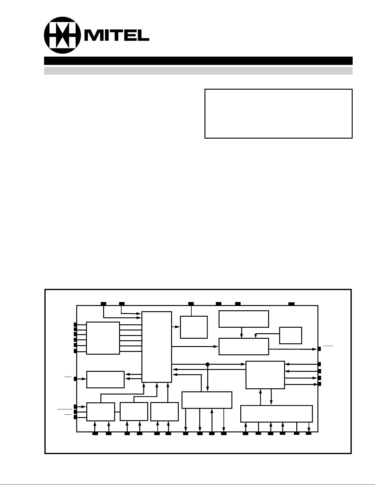
Figure 1 - Functio nal Blo ck Diag ram
SHK
NS
N1
N2
NATT
2-199
Page 2
MH88628 Preliminary Information
TIP
RING
TF1
TF2
RF1
RF2
LGND
LCA
VBat
DCRI
RGND
VRLY
RD
SEL1
SEL2
ESI
ESE
AGND
NATT
N1
1
2
3
4
5
6
7
8
9
10
11
12
13
14
15
16
17
18
19
20
N2
Z900
Z1
Z2
TX
RX
GTX0
GTX1
GRX0
GRX1
ACRI
Z600
NS
SHK
UD
IC
IC
IC
VEE
VDD
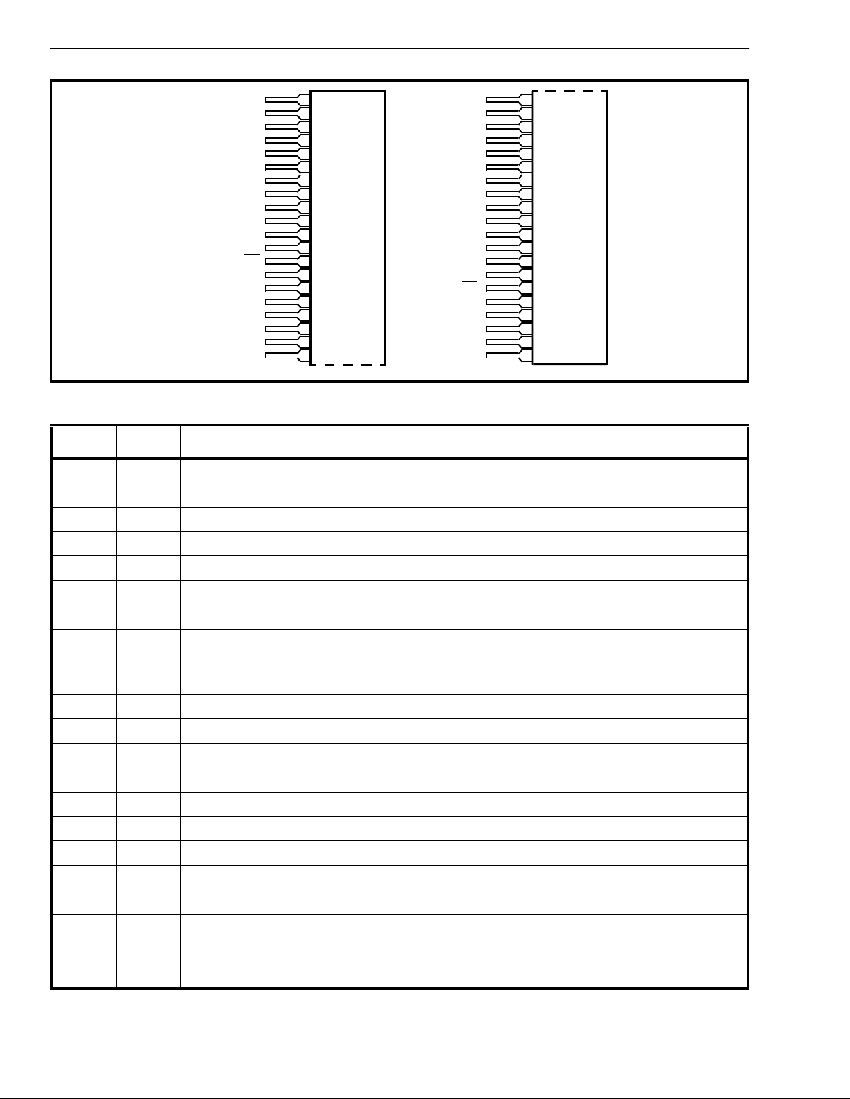
Figure 2 - Pin Connections
Pin Description
Pin # Name
1TIPTip Lead. Connects to the “Tip” lead of subscriber line.
2 RING Ring Lead. Connects to the “Ring” lead of the subscriber line.
Description
21
22
23
24
25
26
27
28
29
30
31
32
33
34
35
36
37
38
39
40
3TF1Tip Feed 1. Access point for balanced ringing. Normall y connects to TF2.
4TF2Tip Feed 2. Access point for balanced ringing. Normall y connects to TF1.
5RF1Ring Feed 1. Access p oint for balanced ringi ng. Norm all y connect s to RF2.
6RF2Ring Feed 2. Access p oint for balanced ringi ng. Norm all y connect s to RF1.
7 LGND Battery Ground. VBat return path. Connected to system’s energy dumping ground.
8LCACurrent Limit Set (Input). The current limit is set by connecting an external resistor to
ground. For 30mA defa ult current, this pin is tied to GND.
9VBatBattery Voltage. Typically -48Vdc is applied to this pin.
10 DCRI DC Ringing Voltage Input. A continu ous 120V dc is applied to this input.
11 RGND R e lay Dri ver Gr oun d Connec tio n.
12 VRLY Relay Supply Voltage Connection.
13 RD
Ring Drive (Output). Connects to ring rel ay coil.
14 SEL1 Sel ect 1 (Inp ut). Refer to Table 5
15 SEL2 Sel ect 2 (Inp ut). Refer to Table 5.
16 ESI External Signal Input. 12/16kHz meter pulse input.
17 ESE External Signal Enable. Applies the external signal to the line.
18 AGND Analog Gr ound. VDD and VEE return path.
19 NATT Network Balance AT+T Node. Connects to N1 for a network balance impedance of AT&T
compromise (350Ω + 1k Ω // 210nF); the device’s input impedance must be set to 600Ω.
This node is active only when NS is at logic high. This node should be left open circuit when
not used.
2-200
Page 3

Preliminary Information MH88628
Pin Description (Continued)
Pin # Name
Description
20 N1 Network Balance Node 1(Input). 0.1 times the impedance between pins N1 and N2 must
match the device’s input impedance, while 0.1 times the impedance between pins N1 and
AGND is the device’s network balance impedance. This node is active only when NS is at
logic high. This node may be terminate d when not used (i.e., NS at logic low).
21 N2 Network Balance Node 2 (Output). See N1 for description.
22 Z900 Line Impedan ce 900Ω Node. Connects to Z1 for a line impedance of 900Ω. This node
should be left open circuit when not used.
23 Z 1 Line Impedance Node 1 (Input). 0.1 times the times the impedance between pins Z1 and
Z2 is the device’s line impedance. This node must always be connected.
24 Z 2 Lin e Impedan ce Nod e 2 (Outpu t). 0.1 times the tim es the impeda nce betwee n pins Z1
and Z2 is the device’s line impedance. This node should be left open circuit when not used.
25 TX Transmit (Output). 4-Wire (AGND) referenced audio output.
26 RX Receive (Input). 4-Wire (AGND) referenced audio input.
27 G TX0 Transmit Gain Node 0. Connects to GTX1 for 0dB transmit gain.
28 G TX1 Transmit Gain Node 1. A resistor to AGND provides transmit gain adjustment.
29 GRX0 Receive Gain Node 0. Connects to GRX1 for 0dB gain.
30 GRX1 Receive Gain Node 1. A resistor to AGND provides receive gain adjustment.
31 AC RI AC Ringing Voltage Input. A 1.5Vrms 20Hz signal is applied to this input.
32 Z600 Line Impedan ce 600
Ω Node (Output). Connects to Z1 for a line impedance of 600Ω.
This pin should be left open circuit when not used.
33 NS Network Balance Setting (Input). The logic level at NS selects the net work balance
impedance. A logic 0 enables an internal balance equivalen t to the input impedance (Z
While a logic 1 enables an external balance 0.1 times the impedance between pins N1 and
AGND balanced to 0.1 times the impedance betwe en pins N1 and N2. The impedan ce
).
in
34 SHK
between N1 and N2 must be equivalent to 10 times the input impedance (Z
Off-Hook Indication (Output). A logic low output indicates when the subscriber equipment
has gone Off-Hook.
35 UD
Unbalance Detect (Output). A log IC low output indicates when the DC current flow in the
Tip and Ring leads is unbalanced, indicating that the subscriber equipment has grounded
the Ring lead.
36,37,38
IC Internal Connection. These pins are internally connected and must be left open
39 VEE Negative Su pp ly Voltage. -5V dc.
40 VDD Positive Supply Voltage. +5V dc.
).
in
2-201
Page 4
MH88628 Preliminary Information
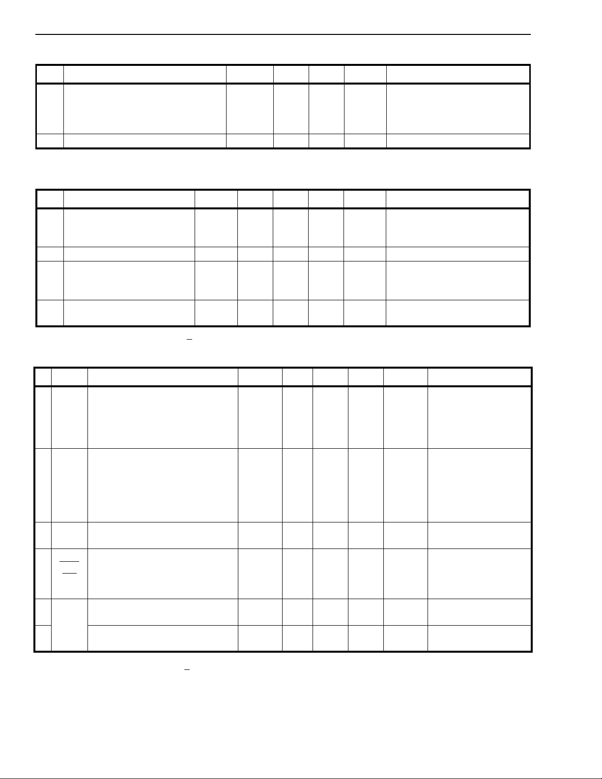
Absolute Maximum Ratings*
Parameter Sym Min Max Units Comments
1 Supply Voltage V
2 Storage Temperature T
* Exceeding these values may cause pe rman ent dama ge. Functi on al operati on under these co ndition s is not implie d.
V
Bat
V
DD
V
DCRI
EE
S
+0.3
-0.3
+0.3
-0.3
65
6
-6
140
-40 +125 °C
V
With respect LG ND
V
V
V
Recommended Operating Conditions
Parameter Sym Min Typ* Max Units Comments
1 Supply Voltage V
2 Operating Temperature T
Bat
V
DD
V
EE
OP
-44
4.75
-4.75
-48
+5.0
-5.0
-60
5.25
-5.25
V
V
V
02070°C
3 AC Ring Generator
Voltage
Frequency 17
90
33
Vrms
Hz
4 DCRI
Input DC Voltage V
* Typical figures are at 25° C with nominal + 5V supplies for design aid only.
DCRI
110 120 130 Vdc
DC Electrical Characteristics‡
Characteristi cs Sym Min Typ* Max Uni t s Test Conditio ns
1 Operating Loop Current
Var in loop current from nominal
2 Operating Currents I
I
Loop
I
Loop
I
Loop
I
Loop
I
I
Bat
Bat
DD
I
3 Power Di ssipation PD
PD
16
EE
O
1
45
30
± 2
32
2
25
25
2
300
4
SHK
UD
5 SEL1
SEL2
ESE
6 High Level Input Current
NS
‡ DC Electrical Characteristics are over recommended operating conditions unless otherwise stated.
* Typical figures are at 25°C with nominal
Low level Output Voltage
High Level Output Vo ltage
Low Level Input Voltage
High Level Input Voltage
Low Level Input Current
+5V supplies and are for design aid only.
V
OL
V
OH
V
IL
V
IH
I
IH
I
IL
3.7
2.4
0.5 V
0.8 V
20
20
mA
mA
mA
mA
mA
mA
mA
mA
W
mW
V
V
µA
µA
=0Ω
R
Loop
2300Ω VBat =-48V
=0Ω, LCA -
R
Loop
GND
R
=0 (off Hook),
Loop
LCA=GND
= open (On-
R
Loop
Hook)
On-hook or Off-Hook
On-Hook or Off-Hook
Active
Standby/Idle
I
= 400µ A
OL
= 40µA
I
OH
VIH=5.0V
=0.0V
V
IL
2-202
Page 5
Preliminary Information MH88628
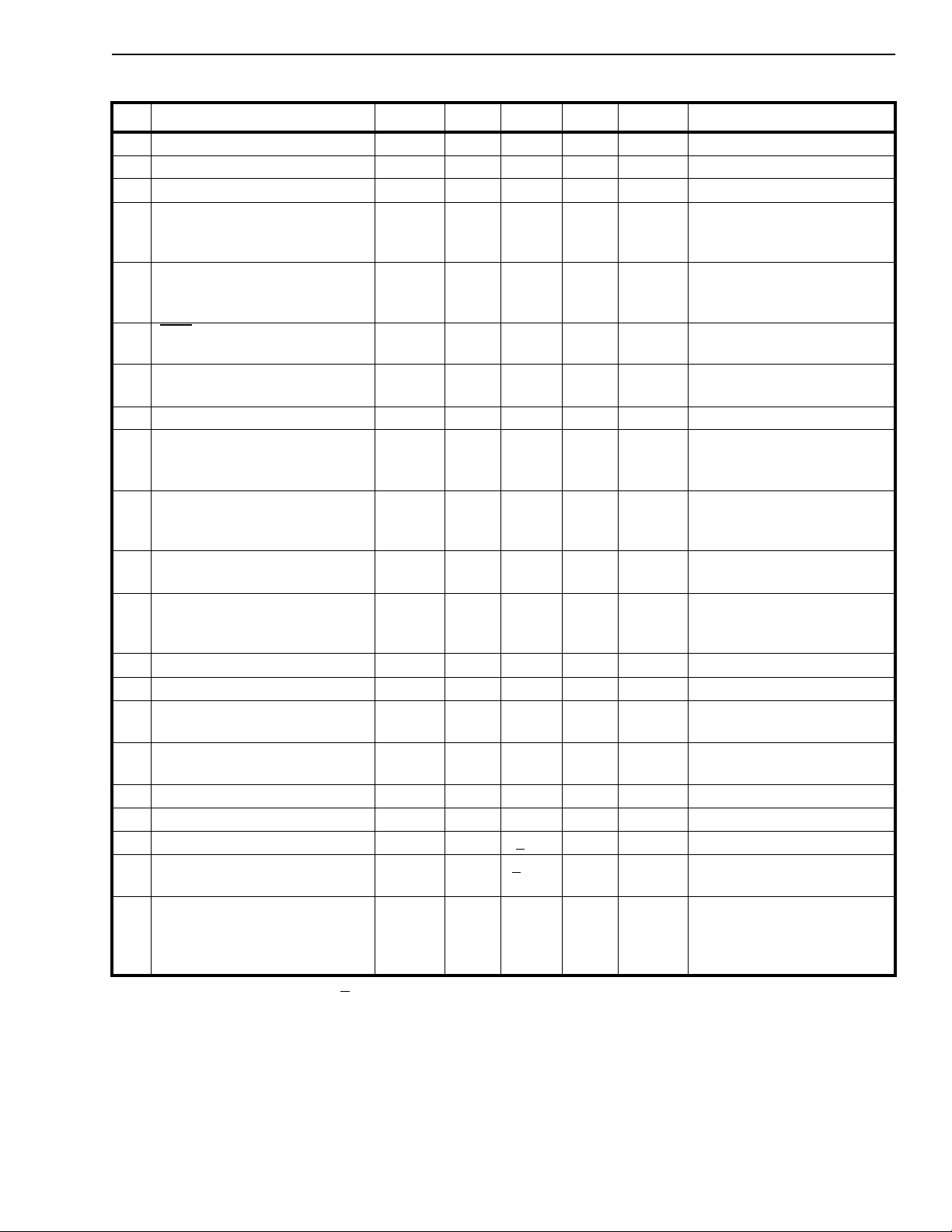
AC Electrical Characteristics‡
Characteristics Sym Min Typ* Max Units Test Conditions
1 TX Gain 0 dB externa l ly adj ustab le
2 RX Gain 0 dB externally adjustable
3 Ringing Capability 5 REN
4 On-Hook Transmission
V
Signal Input Level
Gain 6
5 External S ignal Outp ut Level 1.75 2.25 V
6SHK
Rise Time
Fall time
7 2-Wire Term inat ion
Impedance
t
R
t
F
1
1
600/
900
2.0 V
rms
dB
rms
ms
ms
Ω
8 Off-Hook Det ect Threshold 10 mA
9 2-Wire Return Lo ss 20
20
20
dB
dB
dB
10 Longitudi nal Balance
Longitundinal to Metallic 58
11 Longitudinal Current
53
40 mA 20mA per lead
dB
dB
Capability
12 Idle channel Noise
Rx to T- R
T-R to Tx
N
CR
N
CX
8
12
dBrnC
dBrnC
13 Transhybrid Loss THL 22 40 dB 200-3400Hz
14 Unbalanced Detect Threshold I
UB
10 mA
15 Analog Signal Overload Level
At Tip and Ring 4 dBm
16 Ringing Signal Voltage 90 Vrms
=-48V
Bat
T-R load = 10kΩ min.
V
= -48V, T-R load=
Bat
200Ω LCA=0V, Zo-600Ω,
Gain=0 dB
Dial Pulse De te c ti on
Selectable
300 to 500Hz
500 to 2500Hz
2500 to 3400Hz
200-1000Hz
1kHz - 3k4Hz
T- R=600Ω, V
Bat
=-48V
17 Ringing Frequency 17 33 Hz
18 Ring Trip Delay 100 ms
19 Absolute Gain, Variation +
20 Relative Gai n, refere nce to
0.1 dB 0dB at T-R, 1kHz
+
0.05 dB 300-3400Hz
1kHz
21 Power Supply Rejection Ratio
V
V
V
* Typical figure are at 25°C with nominal +5V supp lies and are for desig n aid only.
‡ AC Electrical Characteristics are over recommended operating conditions unless otherwise stated.
Notes:
Impedance set by external networ k of 600Ω or 900Ω default.
External network for test purposes consists of 2200Ω + 8200 Ω // 11. 5nF between pins Z1 and Z2, the equivalent Zin has 1/10
and is equivalent o 220Ω+820Ω // 115nF.
Test condition uses a Zin value of 600Ω, 900Ω and the above external network.
Test condition s use a transmit and receive gain set to 0dB default and a Zin value of 600Ω unless otherwise stated.
“Ref” indicates reference impedance which is equivalent to the termination impedance.
“Net” indicates ne two rk bala nce impe dance.
Refer to Table 1, 2 for TX, RX gain adjustme nt.
Bat
DD
EE
PSRR
dB 1kHz, 100mVpp
24
24
24
th
the im pe dance
2-203
Page 6

MH88628 Preliminary Information
Functional Description
The SLIC uses a transformerless electronic 2-wire to
4-wire conversion which can be connected to a
Codec to interface the 2 wire subscriber loops to a
time division multiplexed (TDM) pulse code
modulated (PCM) digital switching network. For
analog applications, the Tx and Rx of the 2-4 wire
converter can be connected directly to an analog
crosspoint switch such as the MT8816. Powering of
the line is provided through precision battery feed
resistors. The MH88628 also contains control,
signalling and status circuitry which combines to
provide a complete functional solution which
simplifies the manufacture of line cards. This
circuitry is illustrated in the functional block diagram
in Fig. 1. The MH88628 is designed to be pin
compatible with Mitel’s MH88632 and MH88625.
This allows a common PCB design with common
gain, input impedance and network balance.
Approvals
FCC part 68, CCITT, DOC CS-03, UL 1459, CAN/
CSA 22.2 No.225-M90 and ANSI/EIA/TIA-464-A are
system level safety standards and performance
requirements. As a component of a system, the
MH88628 is designed to comply with the applicable
requirements of these specifications.
Battery Feed
The loop current for the subscriber equipment is
sourced through a pair of matched 200Ω resistors
connected to the Tip and Ring. The two wire loop is
biased such that the Ring lead is 2V above VBat
(typically -46V) and the Tip lead is 2V below LPGD
(typically -2V) during constant voltage, constant
current mode.
The SLIC is designed for a nominal battery voltage
of -48Vdc and can provide the maximum loop current
of 45mA under the condition.
The MH88628 is designed to operate down to a
minimum of 16mA dc, with a battery voltage of -44V.
The Tip and Ring output drivers can operate within
2V o f V
loop range of 2300Ω.
and LGND rails. This permits a maximum
Bat
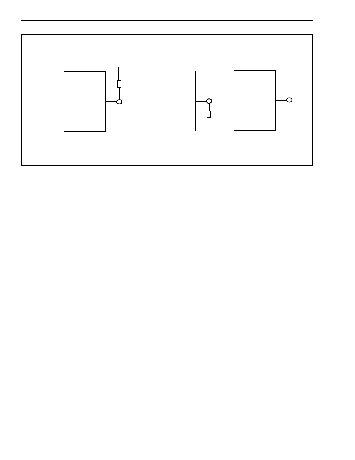
Loop Current Setting
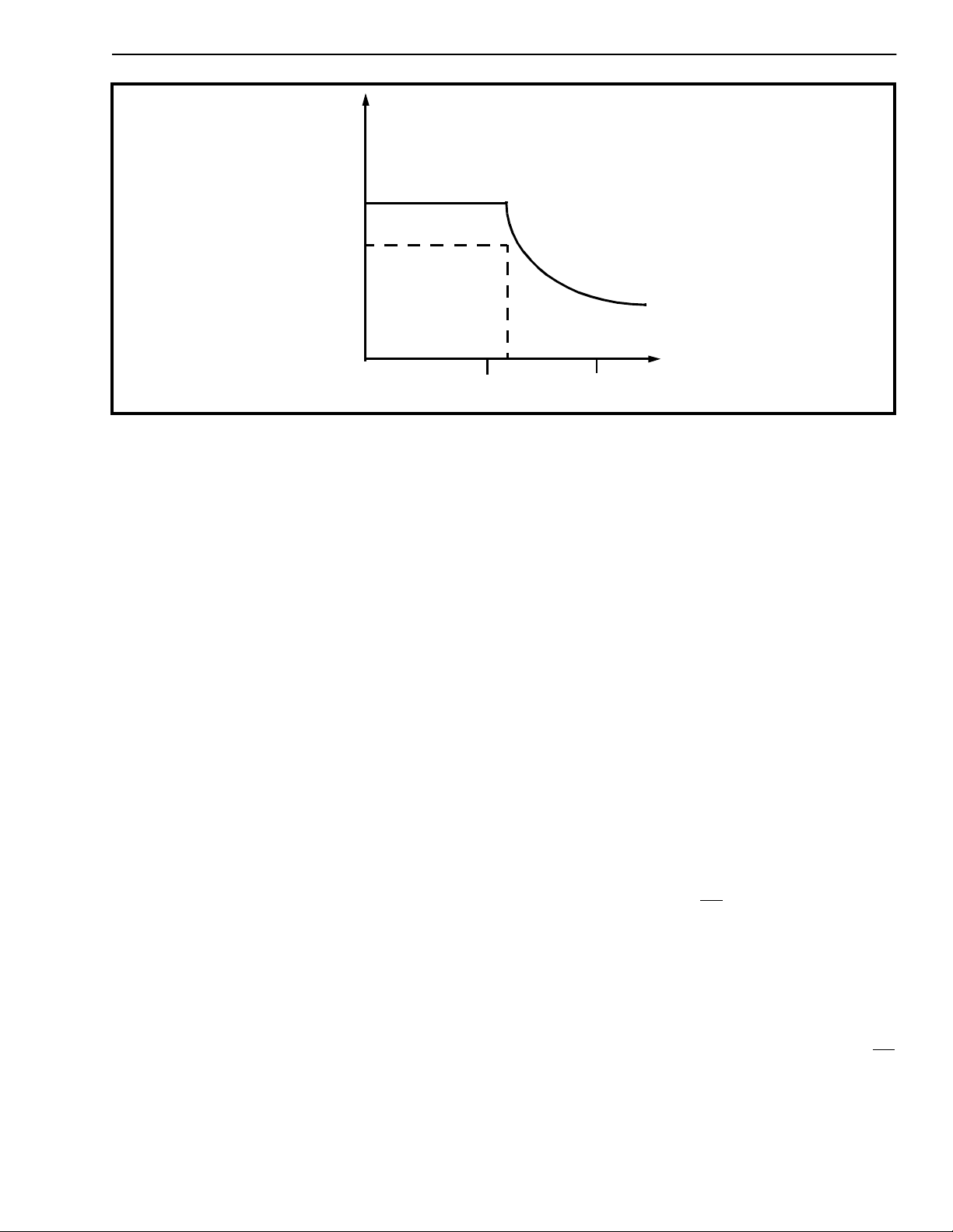
The MH88628 SLIC is a constant current with
constant voltage fallback design. This design feature
provides for long loop capability regardless of the
constant c u rren t se ttin g . Refer to Gra ph 1 .
The LCA (Loop Current Adjust) pin is an input to an
internal resistor divider network which generates a
bias voltage. The loop current is proportional to this
voltage. The loop current can be set between 20 and
45mA by various connections to the LCA pin as
illustrated in Table 5 and Figure 8. The loop current
during a fault condition will be limited to a safe level.
Primary over-current protection is inherent in the
current limiting feature of the 200Ω battery feed
resistors. Refer to Graph 1.
Receive and Transmit Audio Path
The audio signal of the 2-wire side is sensed
differentially across the external 200Ω feed resistors
and is passed on to a second differential amplifier
stage in the 2W/4W conversion block. This block
sets the transmit gain on the 4-wire side and cancels
signals originating from the receive input before
outputting the signal.
Programmable Transmit and Receive
Gain
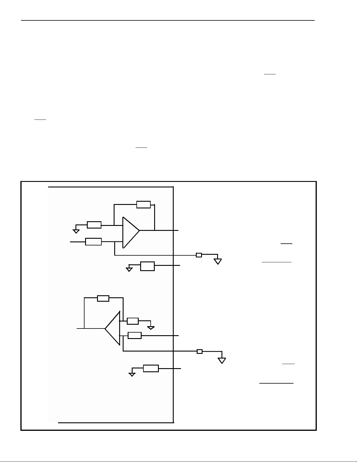
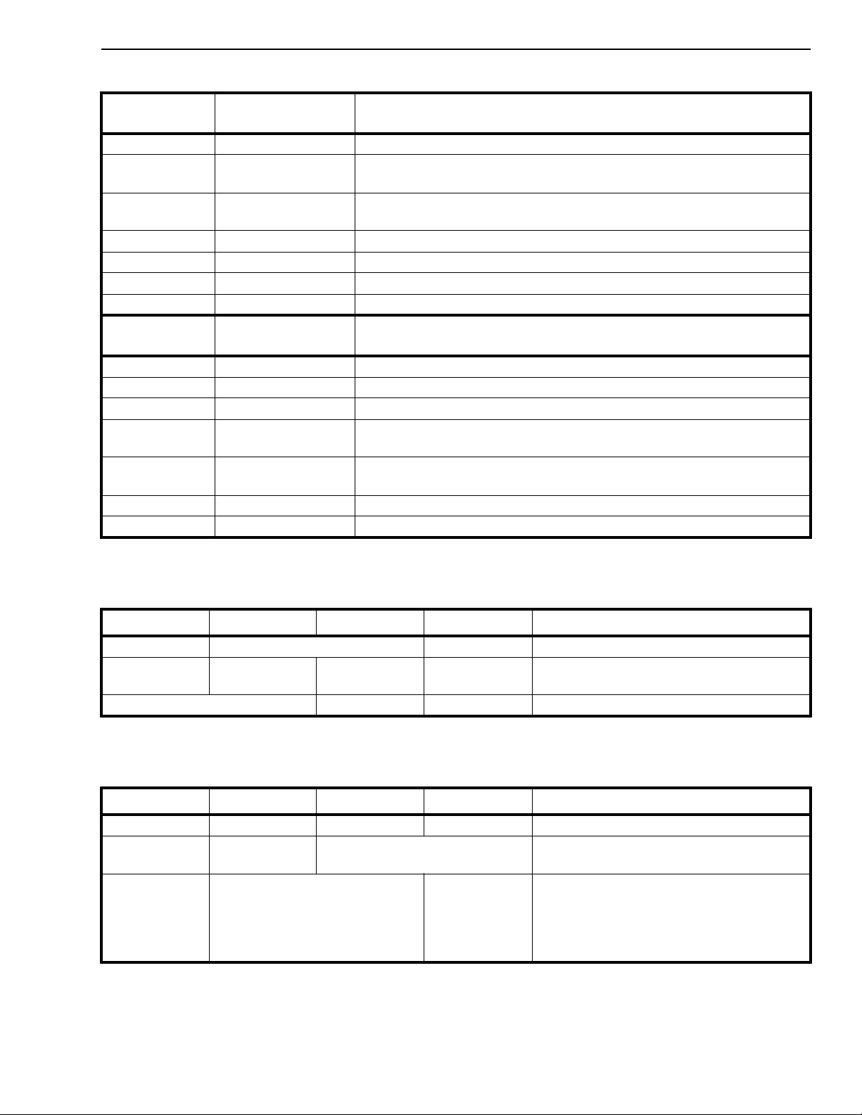
Transmit Gain (Tip-Ring to Tx) and Receive Gain (Rx
to Tip-Ring) are programmed by connecting external
resistors (RRX and RRT) from GRXI to AGND and
from GTX1 to AGND as indicated in Figure 3 and
Tables 1 and 2. The programmable gain range is
from -12dB to +6dB; this wide range will
accommodate any loss plan. Alternatively, the
default Receive Gain of 0dB and Transmit Gain of
0dB can be obtained by connect ing GRX0 to GRX1
and GTX0 to GTX1. In addition, a Receive gain of
+6dB and Transmit Gain of +6dB can be obtained by
not connecting resistors RRX and RTX. For correct
gain programming, the MH88628’s Tip-Ring
impedance (Z
impedance.
For optimum performance, resistor RRX should be
physically located as close as possible to the GRX1
input pin, and resistor RTX should be physically
located as close as possible to the GTX1 input pin.
) must match the line termination
in
2-204
Page 7
Preliminary Information MH88628
70
60
50
Constant
Current Region
I
Loop
(mA)
40
30
20
10
0
Graph 1 - ILoop/RLoop Charac te ristic s
Two wire Port Termination Impedance
The AC termination impedance of 600 or 900Ω, of
the 2W port, is set using active feedback paths to
give the desired relationship between the line
voltage and the line current. The loop current is
sensed differentially across the two feed resistors
and converted to a single ended signal. This signal is
fed back to the Tip/Ring driver circuitry such that
impedance in the feedback path gets reflected t o the
two wire port. The MH88628’s Tip-Ring impedance
) can be set to 600Ω, 900Ω or to a user
(Z
in
selectable value. Thus, Z
can be set to any
in
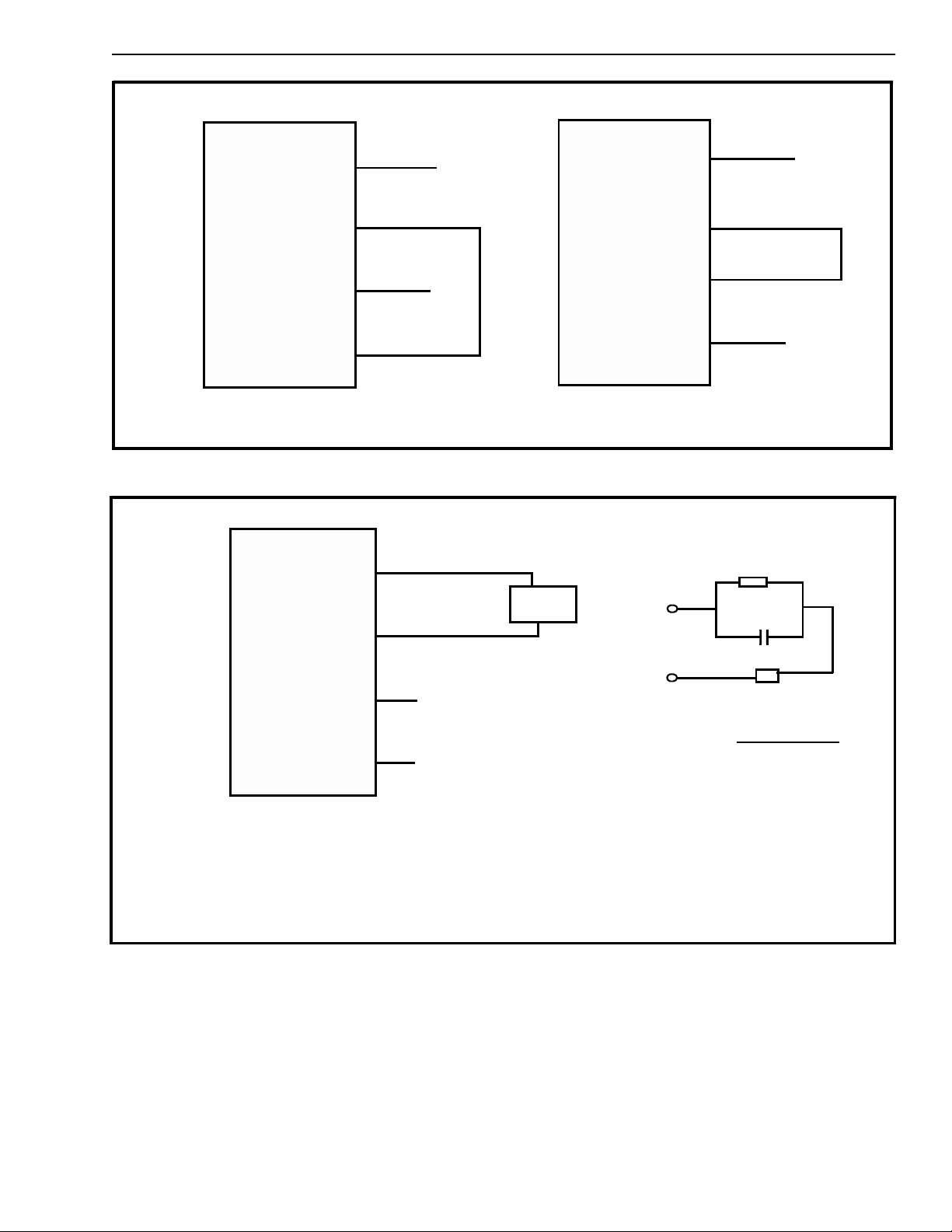
international requirement. The connection to Z1
determines the input impedance. With Z1 connected
to Z600, the line impedance is set to 600Ω. With Z1
connected to Z900, the line impedance is set to
900Ω. A user defined impedance can be selected
which is 0.1 times the impedance between Z1 and
Z2.
For example, with 2200Ω in series with 11.5nF in
parallel with 8200Ω, all between Z1 and Z2, the
devices line impedance will be 220Ω in series with
115nF in parallel with 820Ω. See Table 3 and Figures
4 & 5.
Networ k Balan ce
Transhybrid loss is maximized when the line
termination impedance and SLIC network balance
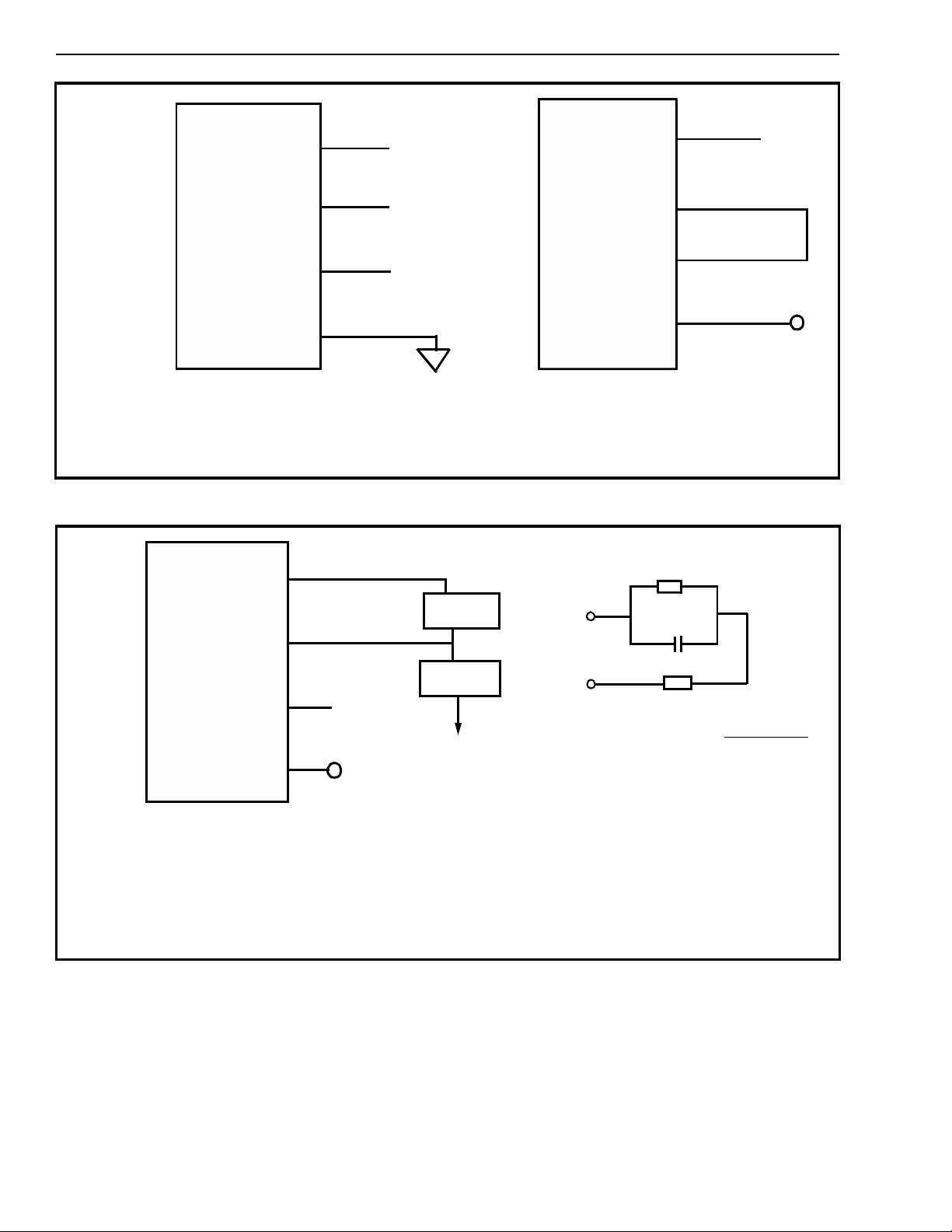
are matched. The MH88628’s network balance
impedance set can be set to Zin, AT&T (350Ω + 1kΩ
//210nF) or to a user selectable value. Thus, the
network balance impedance can be set to any
international requirement, A logic level control input
NS selects the balance mode. With NS at logic low,
an internal network balance impedance is matched
to the line impedance (Z
). With NS at logic high, a
in
1kΩ
Constant
Voltage
Region
R
Loop
2kΩ
(Ω)
user defined network balance impedance is selected
which is 0.1 times the impedance between N1 and
AGND. For example, with 2200Ω in series with
11.5nF in parallel with 8200Ω, all between N1 and
AGND, and NS at logic high, the devices network
balance impedance is 220Ω in series with 115nF in
parallel with 820Ω; the impedance between N1 and
N2 must be equivalent to 10 times the input
impedance (Z
). In addition, with NS at logic high, an
in
AT&T network balance impedance can be selected
by connecting NATT to N1; in this case, no additional
network is required between N1 and N2. See Table 4
and Figure 6.
12/16kHz Meter Pulse
The MH88628 provides control of an external signal
path to the driver. A 12/16kHz continuous signal can
be applied to the ESI pin. Control of the ESE input
allows the metering signal to be transmitted to the
line.
Unbalanced Detection
The Unbalanced Detect (UD) pin goes low when the
DC current through the two battery feed resistors is
unbalanced i.e., when the average DC current into
the Ring lead exceeds the current flow out of the Tip
lead (indicating that the Ring lead has been
grounded).
When the SLIC is interfaced to ground start
subscriber equipment during the idle state, the UD
output is monit ored for indication of the subscribers
Ring Ground signal. The maximum loop current
supplied by the feed circuitry under this condition is
lim ite d.
2-205
Page 8
MH88628 Preliminary Information
Longitudinal Balance
The longitudinal balance specifies the degree of
common mode rejection in the 2 to 4 wire direction.
Precision laser trimming of internal resistors in the
hybrid ensures good overall longitudinal balance.
The interface circuitry can operate in the presence of
induced longitudinal currents of up to 40mA at 60Hz.
Off-Hook and Dial Pulse Detect ion
The SHK pin goes low when the DC-loop current
exceeds a specified level. The threshold level is
internally set by the bias voltage of the switch-hook
detect circuitry. Dial pulse can be detected by
monitoring the interruption rate at the SHK
These dial pulses would be debounced by the
system’s software.
MH88628
pin.
Ring Trip Detection
The interface permits detection of an Off-Hook
condition during the ringing. If the subscriber set
goes Off-Hook when the ringing signal has been
applied, the DC loop current flow will be detected
within approx. 100msecs and the SHK
output will go
low. The ring relay is automatically disabled by the
internal h ard wa r e.
Control Decode
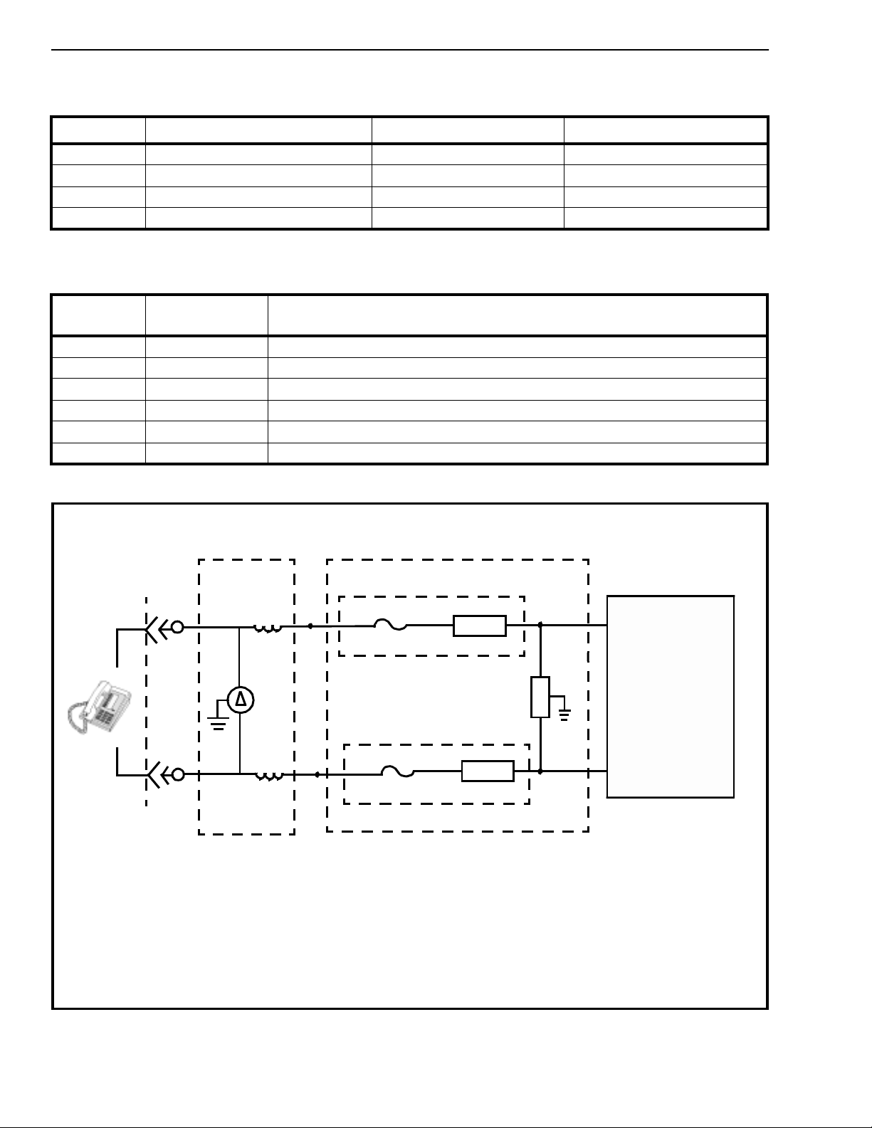
The different modes of operation are selected by
decoding the SEL1 and SEL2 inputs (see Table 5).
DTMF
The DTMF tones are transmitted and received at the
4-wire port.
10kΩ
Z
Transmit Gain:
Z
-
TX
25
+
GTX1
GTX0
10kΩ
Z
28
27
RTX
(Tip-Ring to Tx)
AV= -20log 0.5 + 5kΩ
RTX = 5kΩ
Example
RTX=38kΩ; AV= +4dBV
[
10
(-AV/20)
RTX
-0.5
]
-
26
10kΩ
+
10kΩ
RX
GRX1
GRX0
30
29
RRX
Receive Gain:
(RX to Tip-Ring)
AV= -20log 0.5 + 5kΩ
[
RRX
]
2-206
RRX = 5kΩ
Example:
RRX=4.6kΩ; AV= -4dBV
Figure 3 - Gain Program mi ng with Extern al Comp on ents
10
(-AV/20)
-0.5
Page 9
Preliminary Information MH88628
24
Z2
MH88628
Z900
Z600
Input impedance (Z
Note: Make connection between Z1 and other points as short as possible
) set to 600Ω
in
Z1
23
22
32
NC
NC
Figure 4 - Input Impeda nce (Zin) Settings with Zin equal to 600 or 900Ω
24
Z2
MH88628
Input Impedance (Z
Z2
Z1
Z900
Z600
) set to 900Ω
in
24
23
22
32
10 x Z
RP
NC
NC
in
10 x Z
in
MH88628
Z900
Notes:
1) The 10xZin network must be set to 10 x the desired input impedance (Zin).
2) The network balance must be set to the desired networ k balance. See
section on network balance.
3) Make connection betwee n Z1 and compone nt as short as possible.
Figure 5 - Input Impe dan ce (Z
Z1
Z600
23
22
32
) Settings with Zin not equal to 600 to 900Ω
in
Z2
Z1
= 0.1 x
Z
in
[
RS +
CP
RS
1
1/RP + (S x CP)
]
where S = j x w
and w = 2 x Π x f
Example:
If RS = 2200Ω, RP = 8200Ω, CP= 11.5nf
Then the input impedance ( Z
) is 220Ω in
in
series with 820Ω in parallel with 115nF.
2-207
Page 10
MH88628 Preliminary Information
21
N2
MH88628
NATT
Network balance is set to the input Network balance is set to the AT&T compromise
Impedance (Zin) network (350Ω + 1000Ω // 210nF)
Note: Make connection between Z1 and other points as short as possible
N1
NS
20
19
33
Figure 6 - Network Balance S ettin g with NET BAL eq ual to Zin or AT&T
21
N2
21
N2
MH88628
NATT
impedance. The input impedance must be
set to 600W.
N1
NS
10 x Z
RP
20
19
33
in
VDD
10 x Z
in
MH88628
NA TT
N1
NS
20
19
33
10 x
NETBAL
VDD
Notes :
1) The 10xZin network must be set to 10 x the desired input impedance (Zin).
2) The network balance must be set to the desired networ k balance. See
section on network balance.
3) Make connection betwee n Z1 and compone nt as short as possible.
Figure 7 - Network Balance S ettin g with NET BAL no t equal to Z
N2
N1
ZNETBAL = 0.1 x
where S = j x w
and w = 2 x Π x f
Example:
If RS = 2200Ω
Then the network balance impedance
CP
RS
RS +
[
RP = 8200Ω, CP= 11.5nf
,
1
1/RP + (S x CP)
(ZNETBAL) is 220Ω in series with 820Ω
in parallel with 115nF
in
.
or AT&T
]
2-208
Page 11
Preliminary Information MH88628
Tables 1 & 2: Transmit and Receive Ga in Pro gramm i ng
Transmit
Gain (dB)
+6.0 No Resistor
+4.0 38.3k Results in 0dB overall gain when used with Mitel A-law codec (i.e.
+3.7 32.4k Results in 0dB overall gain when used with Mitel µ-law codec (i.e.
0.0 GTX0 to GTX1
-3.0 5.49k
-6.0 3.32k
-12.0 1.43k
RTX Resistor
Value (Ω)
Notes
MT8965)
MT8964)
Receive Gain
(dB)
RRX Resistor
Value (Ω)
Notes
+6.0 No Resistor
0.0 GRX0 to GRX1
-3.0 5.49k
-3.7 4.87k Results in 0dB overall gain when used with Mitel A-law codec (i.e.
MT8965)
-4.0 4.64k Results in 0dB overall gain when used with Mitel µ-law codec (i.e.
MT8964)
-6.0 3.32k
-12.0 1.43k
Note 1: See Figures 3 and 4 for additional details.
Note 2: Overall gain refers to the receive path of PCM to 2-wire, an d transmi t pat h of 2-wire to PCM.
Table 3: Input Impedance Settings
Z2 Z1 Z600 Z900 Resultin g inpu t imped anc e (Z
NA Connect Z1 t o Z600 N A 600Ω
NA Con nect Z1
to Z9000
NA Connect Z1
to Z900‘
900Ω
Connect network from Z1 to Z2 NA NA 0.1 x impedance between Z1 & Z2
Note 1: NA indicates high impedance (10kΩ) connection to this pin does not effect the resulting network balance.
Note 2: See Figure 4 & 5 for Application Circu its.
)
in
Table 4: Network Balance Settin gs
NS (Input) N2 N1 NATT Resul tin g inpu t im ped anc e (Z
Low NA NA NA Equivalent to Z
High NA Connect N1
to NATT
High Connect network from N1 to
AGND equivalent to 10 x
NA
AT&T compromise (350Ω + 1kΩ // 210nF)
must be 600Ω
Z
in
0.1 x impedance between N1 & N2
NETBAL. Connect ne twork
from N1 to N2 equivalent to 10
x Zin.
Note 1: NA indicates high impedance (10kΩ) connection to this pin does not effect the resulting network balance.
Note 2: Low indicates Logic Low.
Note 3: See Figures 6 and 7 for Application Circuit.
)
in
in
2-209
Page 12
MH88628 Preliminary Information
+5V
R
LCA
8a
Loop Current Setting
Figure 8 - Loop Current Setting
High Volta ge c apability
Inherent in the thick-film process is the ability of the
substrate to handle high voltage. The standard Mitel
thick-film process provides dielectric strengths of
greater than 1000VAC or 1500VDC. The thick-film
process allows easy integration of surface mount
components such as the high voltage bi-polar power
transistor line drivers. This allows for simplier, less
elaborate and less expensive protection circuitry
required to handle high voltage transients and fault
conditions c aused by lightning, induced v oltages and
power line crossings.
On-hook Transmission
The MH88628 provides for on-hook transmission
which supports features such as Automatic N umbers
Identification (ANI). The (ANI) information is a FSK
signal originating from and sent by the C.O. during
the off period of the ringing voltage being sent to the
subscribers set. The s ignal is present during the off
period between the first and second ring. The
subscribers s et decodes the FSK signal and displays
the cal ling part y’s nu mb er.
TIP Disable
A relay driver, controlled by SEL1 and SEL2, is
provided to drive a relay which can be used to
disa ble the TIP line when the MH88628 is used for a
ground start central office interf ac e.
LCA
R
-5V
8b
LCA
8c
Loop Length
The MH88628 can accommodate loop length of up to
2300Ω minimum (including the subscriber
equipment). This corresponds to approximately 8km
using 26AWG twisted pair or 15km using 24AWG
twisted pair.
Central Office Operation
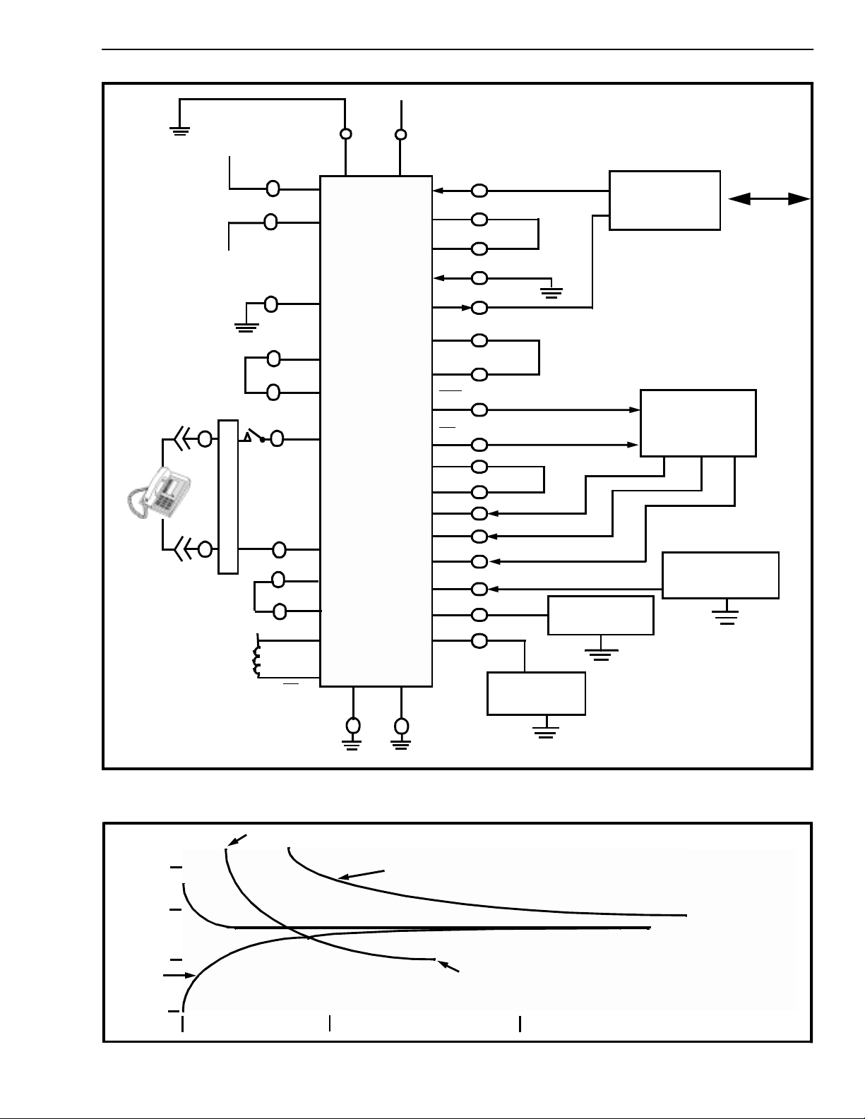
The MH88628 can be configured for ground start
C.O. applications with the addition of Q1, D1 and K2,
as shown in Figure 9. Ground start requires control of
the Tip lead to remove battery ground from
subscriber loop. For loop start applications, control of
the Tip lead is not required.
C.O’s perform Tip/Ring reversals to indicate that a
tool call has been dialled. The Tip/ring reversal can
indicate a toll diversion signal.
Internal Ringing Amplifier Operation
The MH88628 offers an on-board ringing amplifier. A
1.5 VRMS, 20Hz signal is amplified internally and
applied to TIP and RING leads in a balanced
configuration. A +120Vdc supply are applied
continuously to the MH88628. The decode s ignals on
SEL1 and SEL2 enable the ringing signal to the TIP
and RING when required.
2-210
Page 13
Preliminary Information MH88628
-V
Bat
SYSTEM
GROUND
+5V
-5V
O
C
O
R
T
N
P
T
E
I
+5V
K1
K1B
VDD
VEE
AGND
TF1
TF2
TIP
RING
RF1
RF2
VRLY
MH886 28
V
Bat
RX
GRX0
GRX1
LCA
TX
GTX0
GTX1
SHK
UD
Z1
Z600
SEL1
SEL2
ESE
ESI
ACRI
DCRI
VR
VX
1.5VRMS 20Hz
Source
CODEC
LINE
CONTROLLER
LOGIC
12/16kHz
Metering Source
+
RD
Figure 9 - OPS SLIC Con fig urati on Applic atio ns Cir cui t - Norma l Rin ging
Graph 2 - Loop Current Setting
65mA
50
40
Loop/mA
I
30
LCA
= 0V
28.48m
20
10K
RGND
To -5 V
100K
NS
(Ω/10)
To +5V
120VDC
Supply
(Ω/10 + 10mA)
1M
O/C LCA
35.3mA
R(LCA) Ω
2-211
Page 14
MH88628 Preliminary Information
Table 5: Control Decode Table
Mode Condition SEL1 SEL:2
1 Normal Operation 0 0
2 Apply internal balanced ringing 1 0
3 Reverse TIP and RING 0 1
4 Enable Relay Driver 1 1
Table 6: Loop Current Setting
Loop
Current
Ref. Fig # LCA Pin Connectio n
20 8a Connect 10kΩ from LCA to +5V
25 8a Connect 22kΩ from LCA to +5V
30 8a Connect 36kΩ from LCA to +5V
35 8c LCA open circuit
40 8b Connect 24kΩ to -5V
45 8b Connect 10kΩ from LCA to -5V
T
PRIMARY MDF
PROTECTION
HEAT COIL
GAS TUBE
SECONDARY PROTECTION
F1
T
R1
MH88628
PRO1
F2
R
SUGGESTED COMPONENTS:
F1, F2 1A, 250VAC, SLO-BLOW LITTLEFUSE 230 2AG
R1, R2, 10Ω, 1000V, 1/2W RESISTOR (FLAME RATED)
PRO1 SOLID STATE TRANSIENT SUPPRESSOR, EG TISP2300L, P2703AB
F1, R1 AND F2, R2 MAY BE FUSIBLE RESISTORS OR PTCs
HEAT COIL
Figure 10 - Typical Protection Circuit
2-212
R2
R
Page 15
Preliminary Information MH88628
Side View
0.010 +
(0.25 +
Notes:
1) Not to sca le
2) Dimensions in inches).
3) (Dimensions in millimetres).
*Dimensio ns to centre of pin &
tolerance non accumulative.
0.00 2
0.05)
0.080 Ma x
(2.0 Max)
0.12 Max
(3.1 Max)
0.05 +
(1.3 +
0.80+
0.03
0.76)
(20.3+
0.01
0.5)
0.25 +
(6.35 +
1 2 3 4 39 40
1 2 3
0.02
0.05)
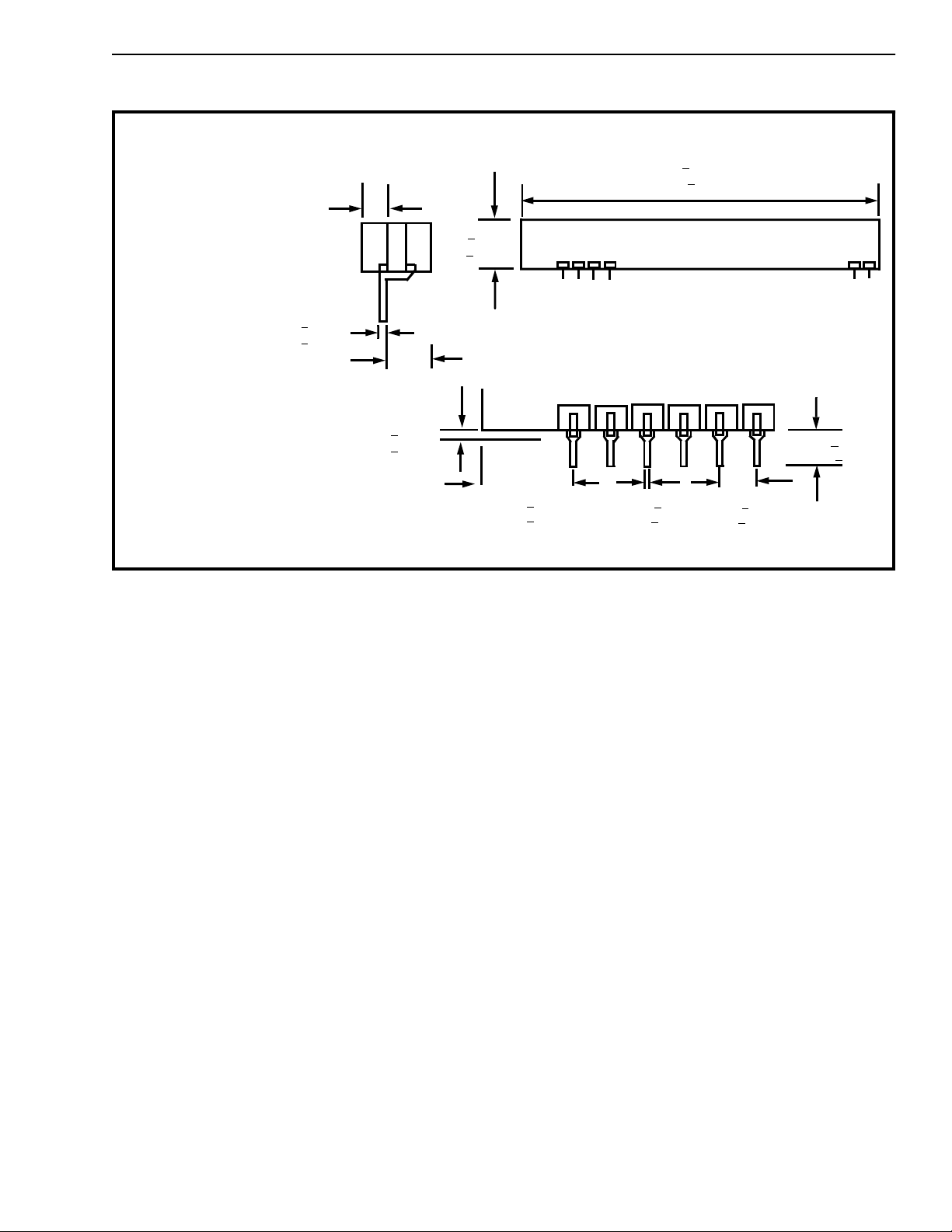
Figure 11 - Mechanical Data
4.20 + 0.0 20
0.5)
(50.8 +
0.175 +
0.02
(4.445 +
***
0.05
0.02 0 +
(0.51 +
0.13)
0.100 +
(2.54 +
0.10
0.13)
0.5)
2-213
Page 16

MH88628 Preliminary Information
Notes:
2-214
 Loading...