

Page 1
MH88622
DUAL OPS SLIC
Preliminary Info rm atio n
Features
•Dual SLIC
• Ringing generation
• On-hook t rans missi on
• Transformerless 2-4 wire conversion
• Constan t c u rrent feed
• Battery Feed to the line
• Tip Ring reversal cap ability
• Over current pro tecti on
• Off-Hook detecti on
• Logic interface for SHK
, RC, LR, ESE, LCS
• Metering injection
•Wide V
operatin g range
Bat
• Minim um in sta lla tio n s pa ce
• ESE ramped output
Applications
•Pair Gain
•CT2
• Cordless local loops
ISSUE 3 April 1995
Ordering Information
MH88622 -1, -2, -3,-5 40 Pin SIL Package
0°C to 70°C
Description
The Mitel MH88622 is a Dual Subscriber Interface
Circuit which provides a complete interface between
the telephone lines a dual codec, requiring a dual rail
supply, battery and dc supply for ringing generation.
The functions provided by the MH88622 includes 2-4
Wire conversion, constant current line feed,
signalling and control. The SLIC manufactured using
thick film hybrid technology which offers high voltage
capability, reliability and high density resulting in a
significant area saving on the printed circuit board. A
complete C.O. type solution can be implemented
with minimal external components. Different variants
are provided to meet different country line
impedance, they are:
-1 220Ω + (820 Ω // 115nF)
-2 600Ω
-3 370Ω + (620 Ω // 310nF)
-5 200Ω + (680 Ω // 100nF)
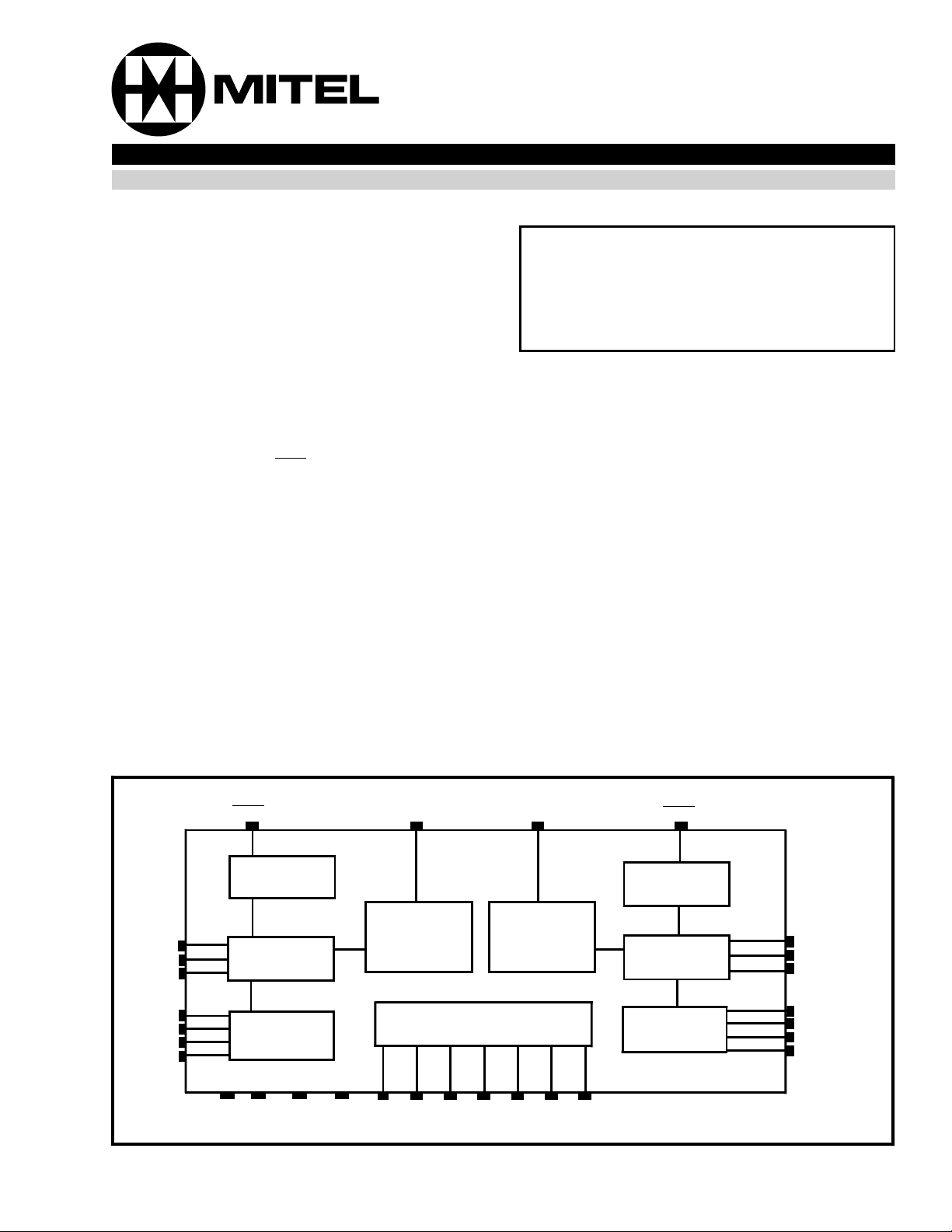
LR1
TIP1
RING1
VX1
VR1
ESI1
ESE1
SHK1
Loop
Supervision
Line Drivers/
Feed
2-4 Wire
Conversion
VDD VEE AGND VBat DCRI RC1 RF1 RF2 RGV RG1 RC2
LCS1
Over Current
Protection &
Constant
Current Feed
Ring Generator
LCS2
Over Current
Protection &
Constant
Current Feed
Figure 1 - Functional Block Diagram
SHK2
Loop
Supervision
Line Drivers/
Feed
2-4 Wire
Conversion
LR2
TIP2
RING2
VX2
VR2
ESI2
ESE2
2-173
Page 2
MH88622 Preliminary Information
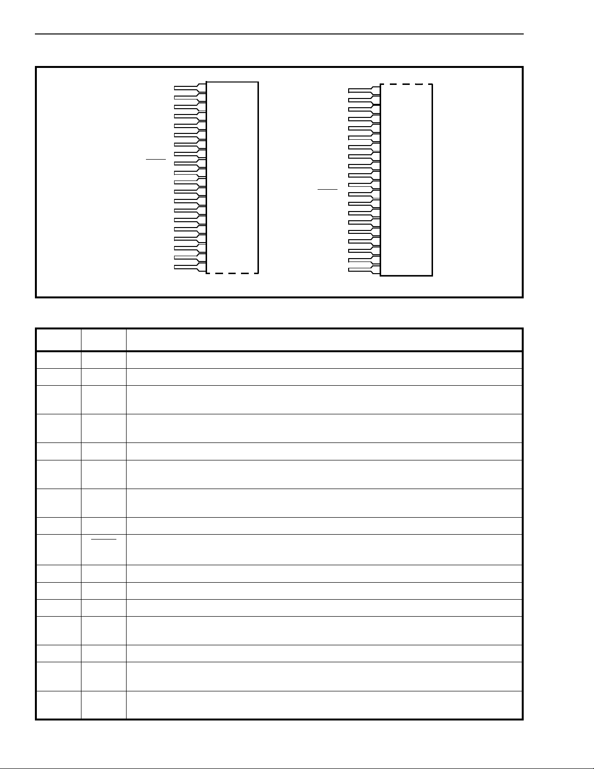
TIP1
RING1
VBAT
DCRI
GND
ESI1
ESE1
VR1
SHK1
LCS1
VX1
VEE
GND
VDD
LR1
RC1
NC
NC
RF1
RF2
1
2
3
4
5
6
7
8
9
10
11
12
13
14
15
16
17
18
19
20
RGV
RG1
NC
NC
RC2
LR2
VDD
GND
VEE
VX2
LCS2
SHK2
VR2
ESE2
ESI2
GND
DCRI
VBat
RING2
TIP2
Figure 2 - Pin Connections
Pin Description
Pin # Name Description
1TIP1Tip Lead. Connects to the “TIP” lead of subscriber line 1.
21
22
23
24
25
26
27
28
29
30
31
32
33
34
35
36
37
38
39
40
2RING1Ring Lead . Connects to the “RING” lead of subscriber line 1.
3V
BAT
Battery V oltage. Typically -48V dc is applied to this pin. This should be connected to pin 38
of the hybrid on the PCB.
4 DCRI DC Ringing Voltage Input. A continuous 120V dc is applied to this input to achieve
90Vrms ringing. This should be connected to pin 37 of the hybrid.
5GNDGround . This pin should be tied to pins 13, 28 & 36 on the PCB.
6ESI1External Signal Input (Input). A continuous signal should be applied to this pin which will
be switched to “Tip” and “Ring” of subscriber 1.
7ESE1External Signal Enable (Input). The external signal to the subscriber 1 is controlled by a
logic level applied to this pin.
8VR1Receive (Input). 4-Wire GND ref erenced audio input for sub scrib er 1.
9SHK1
Off Hook Indication (Outpu t). A logic low out put indicates when subscriber 1 equipmen t
has gone off hook.
10 LCS1 Loop Curr ent Set 1. Logic 1 gives I
= 40mA, Logic 0 gives I
Loop
Loop
= 25mA
11 VX1 Transmit (Output). 4-Wire, GND referenced audio output for subscriber 1.
12 VEE Negative Supply Voltage. -5Vdc. Connects to pin 29 of the hybrid on the PCB.
13 GND Ground . Return path for VDD, VEE, VBat & DCRI. This pin should be connected to pins 5,
28 & 36 of the hybrid on the PCB.
14 VDD Positive Supp ly Voltage. +5Vdc. Connect to pin 27 of the hybrid on the PCB.
15 LR1 Line Reversal. A logic 1 applied to LR1 will reverse the “Tip” and “Ring” to subscriber 1.
This pin has an internal pull down.
16 RC1 Ringi ng Con trol (Inpu t). A logic level applied to this pin enables ringing to be applied
across Tip and Ring of subscriber 1.
2-174
Page 3

Preliminary Information MH88622
Pin Description (Continued)
Pin # Name Description
17 NC No Connection. This pin should not be connected.
18 NC No Connection. This pin should not be connected.
19 RF1 Ring ing Fr equ ency Node 1 (Input). A capacitor is connected betwe en RF1 & RF2 and
determine s the frequency of the ringing generator.
20 RF2 Ring ing Fr equ ency Node 2 (Input). Two capacitors are connected between RF1& RF2
and from RF2 to AGND. This determines the frequency of the ringing generator.
21 RGV Ri ng ing Ga in Voltage. Connects to RG1 through a resistor to reduce the output ringing
voltage. When left open circuit output ringing volt age is 90Vrms.
22 RG1 Ringing Gain Node 1. Connects to RGV thro ugh a resistor to reduce the output ringing
voltage. When left open circuit output ringing volt age is 90Vrms.
23 NC No Connection. This pin should not be connected.
24 NC No Connection. This pin should not be connected.
25 RC2 Ringi ng Con trol (Inpu t). A logic level applied to this pin enables ringing to be applied
across Tip and Ring of subscriber 2.
26 LR2 Line Reversal. A logic 1 applied to LR2 will reverse the “Tip” and “Ring” to subscriber 2.
This pin has an internal pull do wn.
27 VDD Positive Supp ly Voltage. +5Vdc. This pin should be connected to pin 14 of the hybrid on
the PCB.
28 GND Ground . Return path for VDD, VEE, VBat & DCRI. This pin should be connected to pins 5,
13 & 36 of the hybrid on the pcb.
29 VEE Negative Supply Voltage
the PCB.
30 VX2 Transmit (Output). 4-Wire GND referenced audio inpu t for subscriber 2.
31 LCS2 Loop Curr ent Set 2. Logic 1 gives ILoop = 40m A, Logic 0 gives ILoop = 25mA.
32 SHK2
33 VR2 Receive (Input). 4-Wire GND referenced audio input for subscriber 2.
34 ESE2 External Signal Enable (Input). The external signal to subscriber 2 is controlled by a logic
35 ESI2 Exter nal Signal Input. A continuous signal should be applied to this pin which will be
36 GND Ground . This pin should be tied to pins 5, 13 & 28 on the PCB.
37 DCRI DC Ringin g Voltage Input. A continuous 120Vdc is applied to this input to achieve 90
Off Hook Indication (Outpu t). A logic high output indicat es wh en sub scriber 2 equi pme nt
has gone off hook.
level applied to this pin.
switched to “Tip” and “Ring” of subscriber 2.
Vrms ringing. This should be connected to pin 4 of the hybrid on the PCB.
. -5Vdc. This pin should be connected to pin 12 of the hybrid on
38 VBAT Battery Voltage. Typically -48V dc is applied to this pin. This should be connected to pin 3
of the hybrid on the PCB.
39 RING2 Ring Lead. Connects to the “Ring” lead of subscriber line 2.
40 TIP2 Tip Lead. Connects to the “Tip” lead of subscriber line 2.
2-175
Page 4
MH88622 Preliminary Information
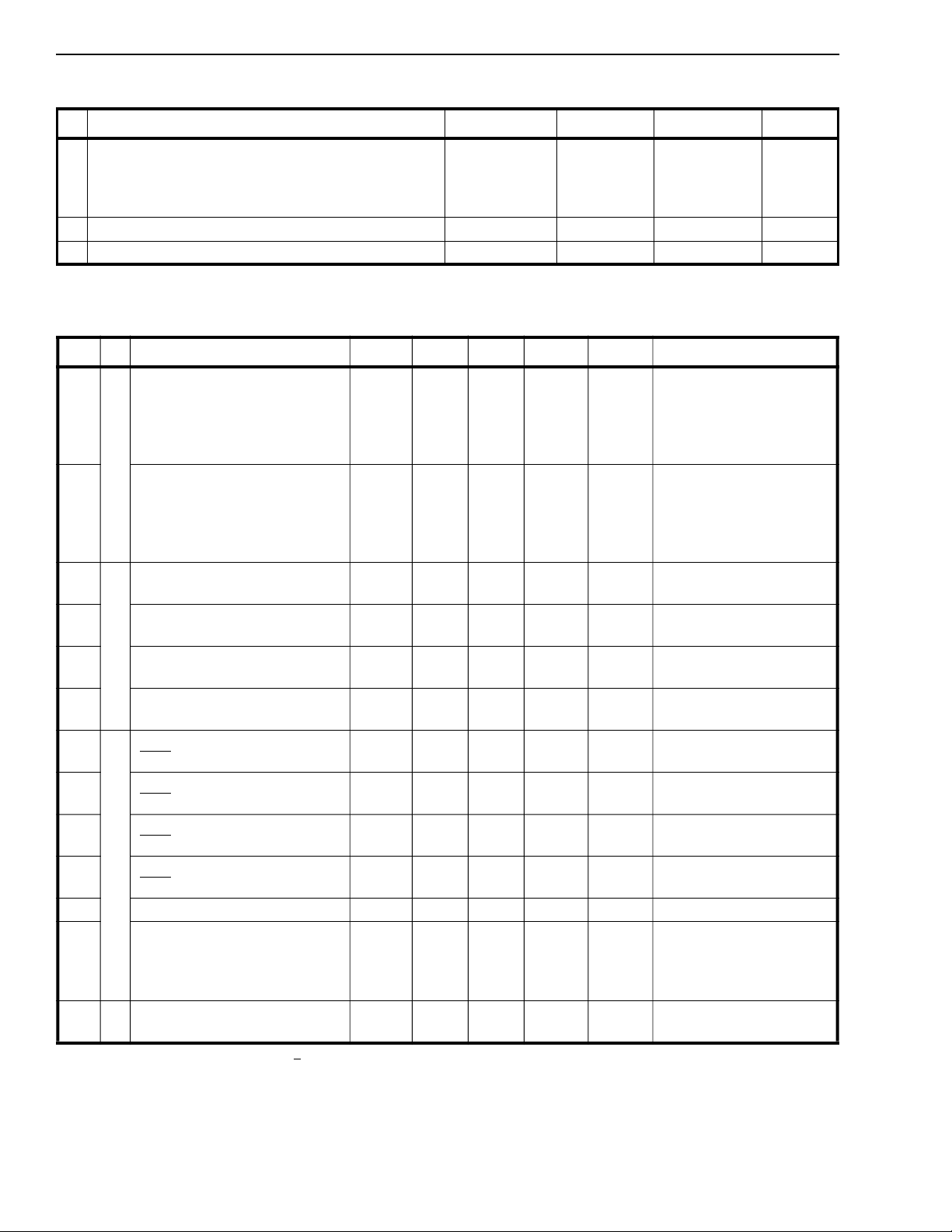
Absolute Maximum Ratings *- All voltages are with respect to GNDA unless otherwise stated.
Parameter Symbol Min Max Units
1 Supply Voltages - Referenced to V
(GN D ) V
SS
V
EE
V
DD
DCRI
V
Bat
+0.3
-0.3
-0.3
-60
-15
+15
+180
0.3
2 Operating Temperature TAMB -40 +85 °C
3 Storage Temperature T
* Exceeding these values may cause perman ent dama ge. Functi onal operati on under these cond ition s is not implied.
S
-55 +12 5 °C
DC Electrical Characteristics
1
2
3
4
5
6
7
8
9
10
11
12
13
Characteristics Sym M in
Operating Loop Current V
S
U
P
P
Operating Supply Current
L
(per Channel)
Y
High Level Input Voltage LR,
I
RC, ESE, LCS
N
Low Level Input Voltage LR,
P
RC, ESE, LCS
U
High Level Input Current LR,
T
RC, ESE, LCS
S
Low Level Input Current LR,
RC, ESE, LCS
High Level Output Current
O
SHK
U
Low Level Output Current
T
SHK
P
High Level Output Voltage
U
SHK
T
Low Level Output Voltage
S
SHK
Constant Current Line Feed I
Maximum Operating Lo o p R
Power Consumption P
V
V
V
I
DCRI
V
V
EE
DD
DCRI
Bat
I
EE
I
DD
I
Bat
V
IH
V
IL
I
IH
I
IL
I
OH
I
OL
OH
OL
Loop
L
C
‡
Typ* Ma x
-4.75
4.75
110
-60
-5
5
120
-48
30
30
15
5
4.5 V
4.75 V
23 25 27 mA LCS = 0
‡
Units Test Comments
-5.25
5.25
160
-20
V
V
V
V
mA
mA
mA
On-hook
On-Hook
Ringing
(REN=1)
mA
Idle
0.5 V
700 µA
10 µA
0.4 mA
4mA
0.4 V
500
1500
Ω
Ω
@ 25mA -24V
@ 25mA -48V
inclusive of telephone
set
300 mW Excluding P
BAT
& P
V
V
V
V
DCRI
* Ty pical figures are at 25°C with nominal +5V supplies and are for desig n aid only.
‡
Max & Min figures guaranteed over 0°C to 70°C only
2-176
Page 5
Preliminary Information MH88622
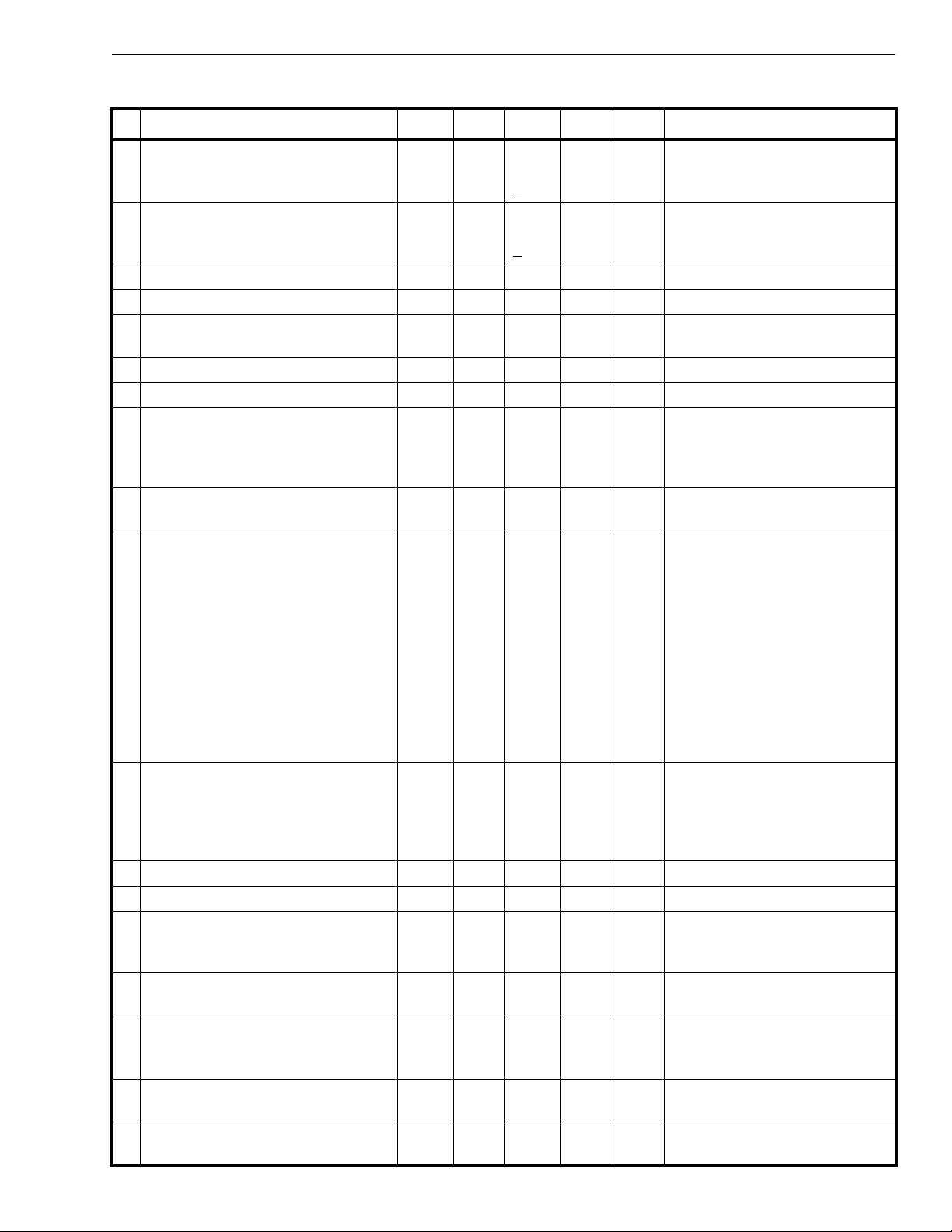
AC Electrical Characteristics*
Characteristics Sym Min‡Typ†Max‡Units Test Comments
1 Gain VR to 2-Wire
Gain relative to Gain @ 1kHz
2 Gain 2-wire to VX
Gain relative to Gain @ 1kHz
-0.2 0
+
0.15
-6.2 -6
0.15
+
+0.2 dB Input 1.0Vrms 1kHz @ VR,
Zload = Z
in
300-3.4kHz
-5.8 dB Input 3dBm 1k Hz @ 2W
Zsource = Z
in
300-3.4kH z
3 Off-Hook Detect Threshold 7.5 mA
4 Transhybrid Loss THL 22 30 dB 300-3.4kHz
5 Ri nging Signal Voltage 40 Vrms Min 65Vdc differential bet ween
DCRI & V
BAT
6 Ringing Freq uency 17 68 Hz See Table 1
7 Ringing Capa bilit y 4 REN 1750Ω impedance @ 20Hz min.
8 Power Supply Reject ion Rat io
VDD/V
V
V
Bat
EE
DCRI
PSRR
30
30
30
dB Ripple
0.1 VPP 1kHz
9 2-wire Return Loss 20 35 dB Input 0.5 Vrms 1kHz across Tip
10 Longitudinal to Metallic Balance
-1 Variant
-2 Variant
-3 Variant
-5 Variant
40
55
53
58
53
46
40
46
& Ring Zload = Z
Input 0.5Vrms
dB
50-300Hz
dB
300-1000Hz
dB
1k-4kHz
dB
200Hz to 1kHz
dB
3kHz
dB
300Hz to 3k4Hz
dB
300Hz to 600Hz
dB
600Hz to 3k4Hz
in
Metallic to Longitudinal Balance
-2 Variant only
11 Input AC Impedance (2- wire)
-1 variant (220Ω + 820Ω // 115nF)
-2 variant (600Ω)
-3 variant (370Ω + 620Ω // 310nF)
-5 variant (200Ω + 680Ω // 100nF)
Z
60
40
IN
dB
200Hz to 1kHz
dB
1kHz to 4kHz
Ω 1kHz @ 2-wire
600
900
700
823
12 Input Impedance @ VR 230 kΩ
13 Output Impedance @ VR 10 Ω
14 Total Harmonic Distortion
at VX
at Tip & Ring
15 Common Mode Rejecti on
THD
0.2
0.2
%%Input 4dBm @2-Wire
Input 1V at VR
CMRR 40 60 dB Input 0,5V, 1kHz
Ratio 2-Wire to VX
16 Idle Channel Noise
at VX
at 2-wire
17 On-Hook Transmission Signal
Input Level Gain 6
18 External Signal Out put Lev el 1.75 2. 2 Vrms V
NC
15
15
dBrn
C
2.0 VrmsdBV
= -48V
Bat
T-R load = 10kΩ min.
= -48V
Bat
T-R load = 200Ω
2-177
Page 6
MH88622 Preliminary Information
AC Electrical Characteristics* (Continued)
Characteristics Sym Min‡Typ†Max‡Units Test Comments
19 SHK
20 Analogue Signal Overload Level
Rise Time
Fall Time
t
R
t
F
1
1
msmsDial Pulse
Detection
4dBm@ 1kHz
@ Tip & Ring
21 Ring Trip Delay 100 ms
22 Outband Noise No -70 dB Refer to BS6305 section 4.1.4 &
fig 3 for details of limits
23 Crosstalk Channel 1 to 2
Channel 2 to 1
* AC Electrical Characteristics are over Recommended Operating Conditions unless otherwise stated.
† Typical figures are at 25°C with nominal + 5V suppli es and are for design aid only.
‡ Max and Min figures guaranteed over 0°C to 70°C only.
Notes: Impedance set to variant impedance
Test conditi on s us es a Z
Test conditi on s us e a transmi t a nd receive gain set to 0dB def au lt a nd a Z
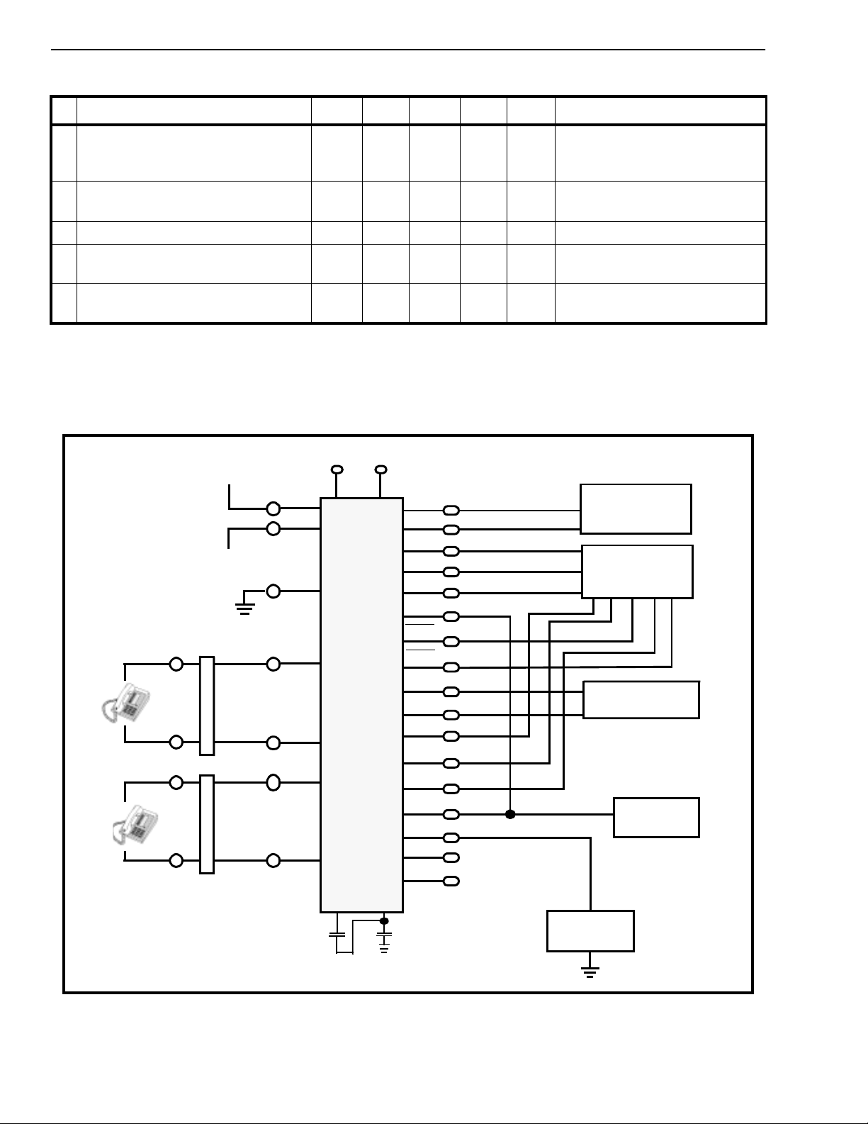
SUBSCRIBER 1
value as specified by variant number.
in
V
DCRI
+5V
V
DD
V
EE
-5V
GND
TIP1
V
Bat
VR1
VX1
RC1
LR1
ESE1
ESI1
SHK1
SHK2
-80
dBdB@ 1kHz
-80
value of 600Ω unl es s ot he rw is e st ated.
in
CODEC
SUBSCRIBER 1
LINE
CONTROLLER
LOGIC
.
SUBSCRIBER 2
RING1
TIP2
RING2
CF1
RF1
VR2
VX2
RC2
LR2
ESE2
ESI2
DCRI
RGV
RG1
RF2
CF2
CODEC
SUBSCRIBER 2
120VDC
SUPPLY
Figure 3 - Loop Start SLIC Con fig ura tion Appl i catio n Circui t
12/16kHz
SOURCE
2-178
Page 7
Preliminary Information MH88622
Functional Description
The SLIC uses a Transformerless 2-4 Wire converter
for each subscriber which can be connected to a
CODEC to interface the 2-Wi re subscribe r loop to a
time division multiplexed (TDM), pulse code
modulated (PCM), digital link.
Powering of the subscriber line is provided through
precision battery feed resistors on the hybrid. The
thick film hybrid circuit contains control, signalling
and status circuits which combine to provide a
complete solution simplifying the manufacture of line
cards.
Approvals
FCC part 68, CCITT, DOS CS-03, UL 1459, CAN/
CSA-22.2 N0. 225-M9 0 an d AN SI/EIA/TIA-4 6 4 -A are
system level safety standards and performance
requirements. As a component of a system, the
MH88622 is designed to comply with the applicable
requirements of these specifications.
Two Wire Port Termination Impedanc e
The Tip/Ring impedance (Zin) is fixed for each
variant.
Transmit and Rece ive G ain
The transmit and receive gain of the MH88622 is
internally set.
Internal Ringing Generator
The MH88622 offers an on board ringing generator
requiring only two external passive components and
a DC voltage source to produce a sine wave of
betwee n 17Hz to 68Hz.
An internal signal is amplified by a user program med
amount and is applied to Tip and Ring. The
programmable gain must be s et using RGV and RG1
to ensure that distortion of the ringing signal is
minimised.
Battery Feed
The SLIC is designed for a nominal battery voltage
of -48 Vdc and can provide the constant feed current
for 1500Ω loop under this condition.
The interface circuit is designed to be operated up to
a maximum of -60V dc battery feed voltage without
damage, providing a minimum loop length capability
of 2000 Ω.
There is also a function on the SLIC that provides for
Tip-Ring reversal.
Current Limit
Primary over current protection is inherent in the
current limiting feature of the battery feed circuit.
Current limiting is provided for both Tip and Ring
unbalan ced cond i ti ons.
The maximum loop current limit is set internally on
the interface and current limiting does not affect the
longitudinal or the signal balance of the device. To
set I
set I
or tied low (Logic 0).
to 40mA tie the LCS pin high (Logic 1), to
Loop
to 25mA the LCS pin may be left open circuit
Loop
With V
ringing voltage = 90Vrms RGV and RG1 shoul d be left
open circuit. By adding an external resistor between
RGV and RG1 it is possible to reduce the ringing
voltage applied by the driver section to Tip and Ring.
The DC voltage source should be continuously applied
to the MH88622. The ringing voltage will only be
applied when the RC pin of the relevant subscriber is
activated.
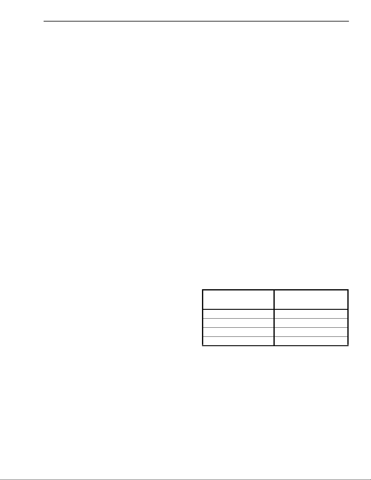
Table 1 - Ring G ener ator C apacito r Sel ection
= -48Vdc and V
BAT
T yp. Frequency
(Hz)
17 100
25 68
35 47
50 33
= +120Vdc and the
DCRI
CF1, CF2
(nF)
12-16kHz Meter Pulse
The MH88622 provides control of an external signal
path to the driver. A 12/16 KHz continuous signal
should be applied to the ESI pin. Control of the ESE
input allows the metering signal to be transmitted to
the line with a ramped up and down amplitude to
reduce noise on the line. Typical ramp time is 10mS.
2-179
Page 8
MH88622 Preliminary Information
Off-Hook and Dial Pulse Detect ion
The SHK pin goes low when e DC loop current
exceeds a specified level. The threshold level is
internally set by the bias voltage of the switch hook
detect circuit.
Dial pulse can be detected by monitoring the
interruption rate at the SHK
need to be debounced by the systems software.
pin. These dial pulses may
Ring Trip Detecti on
The interface permits detection of an Off-Hook
condition during ringing. If the subscriber set goes
Off-Hook when the ringing signal has been applied,
the DC loop current flow will be detected within
approx. 100msecs and the SHK
The ringing is automatically disabled by the internal
hardware .
output will go low.
Longitudinal Balance
Precision laser trimming of resistors in the hybrids
ensures good overall longitudinal balance.
High Vol tage Capability
Inherent in the thick film process is the ability of the
thick film process dielectric strengths of greater than
1000 VAC or 1500 VDC. The thick film process
allows easy integration of surface mount
components such as the high voltage bi-polar power
transistor line drivers. This allows for simpler, less
elaborate and less expensive protection circuitry
required to handle high voltage transients and fault
conditions caused by lightening, induced voltages
and power line crossing.
On Hook Transmission
The MH88622 provides for on-hook transmission
which supports features such as Automatic Number
identifications (ANI).
Loop Length
The MH88622 can accommodate loop length of up to
2000Ω minimum (including the subscriber
equipment).
The interface circuitry can operate in the presence of
induced longitudinal currents of up to 40mA rms at
60Hz.
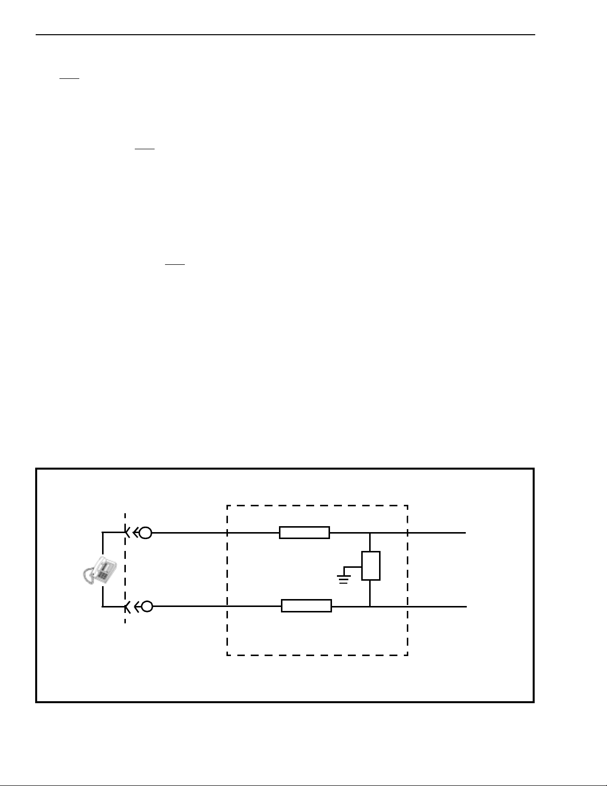
T
R
PROTECTION
PTC
RESISTOR
5 Ohms
PTC
RESISTOR
5 Ohms
T
TISP2290
or
P2702AB
R
2-180
Figure 4 - Typical Protection Circuit
Page 9
Preliminary Information MH88622
0.002
0.010 +
0.05)
(0.25 +
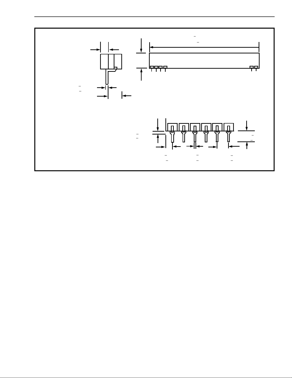
Notes:
1) Not to scale
2) Dimensions in inches).
3) (Dimensions in millimetres).
*Dimension s to centre of pin &
tolerance non accumulative.
0.25 Max
(6.4 Max)Side View
0.27 Max
(6.9 Max)
0.95 Max
(24.13 Max
0.05 +
(1.3 +
0.5)
0.02
*
4.2 + 0.03
(107 + 1)
23
1
43940
0.180 +
0.02
*
(4.6 +
0.5)
0.02 0 +
0.05 +
(1.27 +
0.02
0.5)
0.00 5
(0.51 + 0.13)
0.100 +
(2.54 +
0.010
0.26)
Figure 5 - Mechanical Data
2-181
Page 10

MH88622 Preliminary Information
Notes:
2-182
 Loading...