

Page 1
MH88500
Hybrid Subscriber Line Interface Circuit (SLIC)
Preliminary Information
Features
• Differential to s ingle en ded conv ersion
• No transforme rs req uired
• Minim um in sta lla tio n s pa ce
• Off-Hook detection and LED indicator drive
• Relay drive outp ut
• Battery and ri ngin g feed to line
• Logic interface: MUTE
, OFHK, RC
• Mute of inco ming aud io
• Dial pulse detection
• Voltage surge protecti on
Applications
Line Interfac e for:
• PABX
• Intercoms
• Key System s
ISSUE 5 April 1995
Ordering Information
MH88500 20 Pin SIL Packa ge
0°C to 70°C
Descript io n
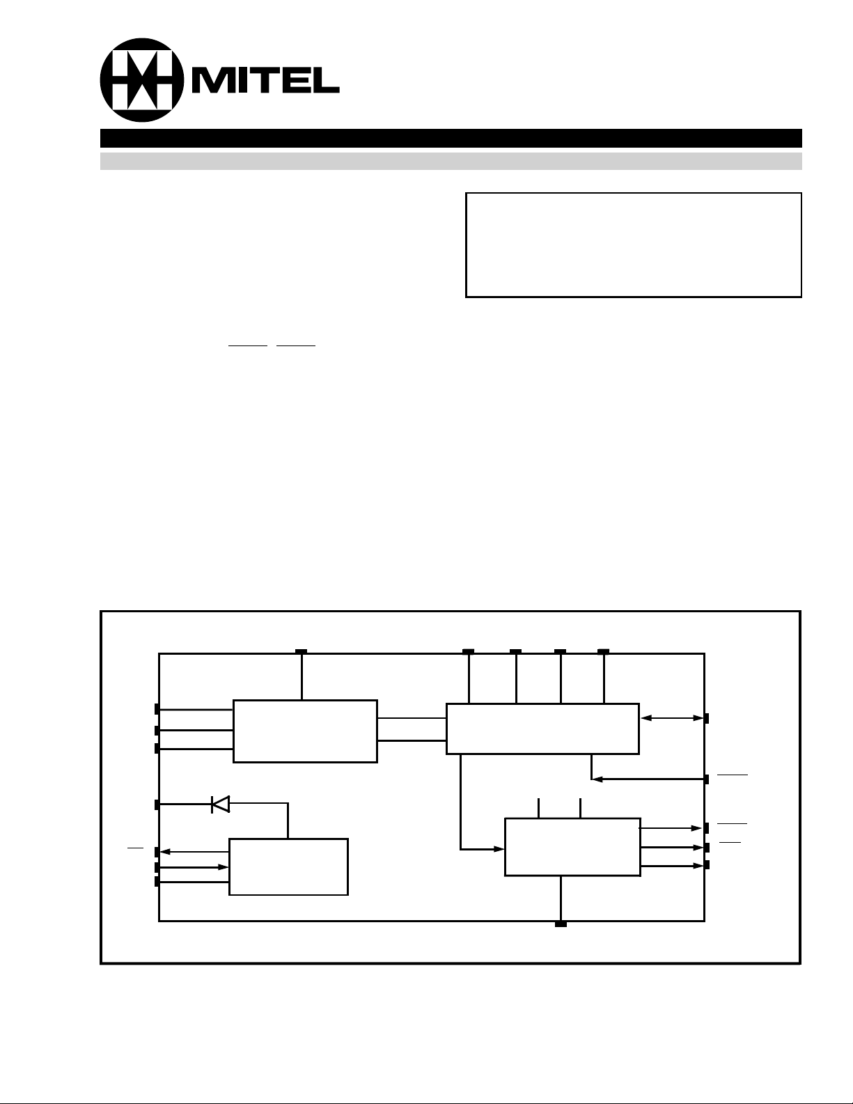
The Mitel MH88500 Subscriber Line Interface Circuit
provides a complete interface between the telephone
line and a speech switch requiring only single
bidirectional switch per crosspoint. The functions
provided by the MH88500 include bidirectional
differential to single ended conversion in the speech
path, line battery feed, ringing feed and loop and dial
pulse detection. The device is fabricated as a thick
film hybrid in a 20-pin ‘single-in-line’ package
allowing optimum circuit board packing density.
TIP
RING
RING
FEED
CD
RD
RC
RGND
VA
Loop Feed/
Ring Feed
Relay Drive
Circuit
V
1
A2
Figure 1 - Functional Blo ck Diag ram
V
Speech Circuit
V
B
C1
V
A2
Loop Detectio n
V
C2
GND
JUNCTOR
V
B
MUTE
OFHK
LED
THRESH ADJ
2-33
Page 2
MH88500 Preliminary Information
TIP
VA1
RING
RING FEED
THRESH ADJ
IC
VC1
GND
V
LED
OFHK
VA2
GND
VC2
MUTE
JUNCTOR
RD
RGND
RC
CD
B
1
2
3
4
5
6
7
8
9
10
11
12
13
14
15
16
17
18
19
20
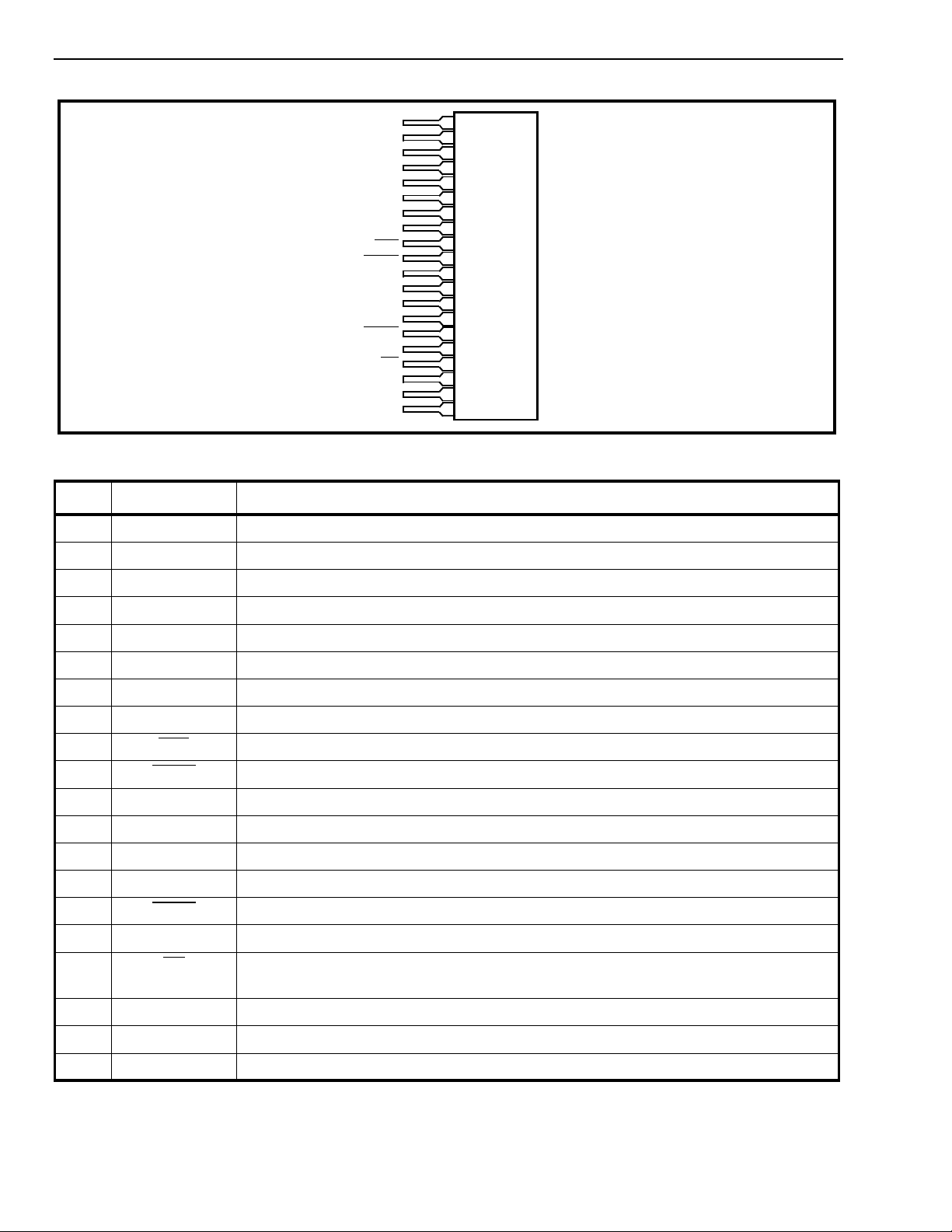
Figure 2 - Pin Connections
Pin Description
Pin # Name Description
1TIPTip Lead. Connects to the “Tip” lead (A-wire) of the telephone line.
2V
A1
3RINGRing Lead. Connects to the “Ring” lead (B-wire) of the telephone lin e.
Positive Li ne Fe ed S upp ly Voltag e. Normally connected to VA2.
4 RING FEED Negative Li ne Feed Voltage and Ringing Input. Normall y connected to Ring Relay.
5ICInternal Connection. Leave open circuit. Use for testing only.
6V
C1
Sense Inpu t. Normally connected to negative line fe ed voltag e supply.
7GNDAnalog ground (0V). Internally co nnecte d to pin 13.
8V
B
9LED
10 OFHK
Negative Anal og Suppl y Voltage.
LED Dr ive Output. Drives an LED directly. Off-Hook condition, logic low.
Logic Low Output. Indicates closed loop condition (Off-Hook and dial pulsing).
11 THRESH ADJ Allows a djustment of OFHK detect ion th resh old.
12 V
A2
Positive P owe r Suppl y Voltage. Normally connected to VA1.
13 GND Analog Ground (0V). Internally connected to pin 7.
14 V
C2
15 MUTE
Loop Detector Voltage Supply.Connected to negative line feed voltages supply.
Input mutes the incom in g audio. Active lo w.
16 JUNCTOR Receive/tr ansm i t audio sp eech pa th. (referenced to 0V GND)
17 RD
Relay Drive Output. Open collector sink s current when RC high. Diode clamp
protecte d.
18 RGND Ground for Relay Drive Circui t .
19 RC Ring Control Input. Active high.
20 CD Clampin g Dio de. Normally connected to relay positive voltage.
2-34
Page 3
Preliminary Information MH88500
Functional Description
Speech Circuit
The speech circuit converts the bidirectional TIP and
RING line pair to a bidirectional single ended junctor
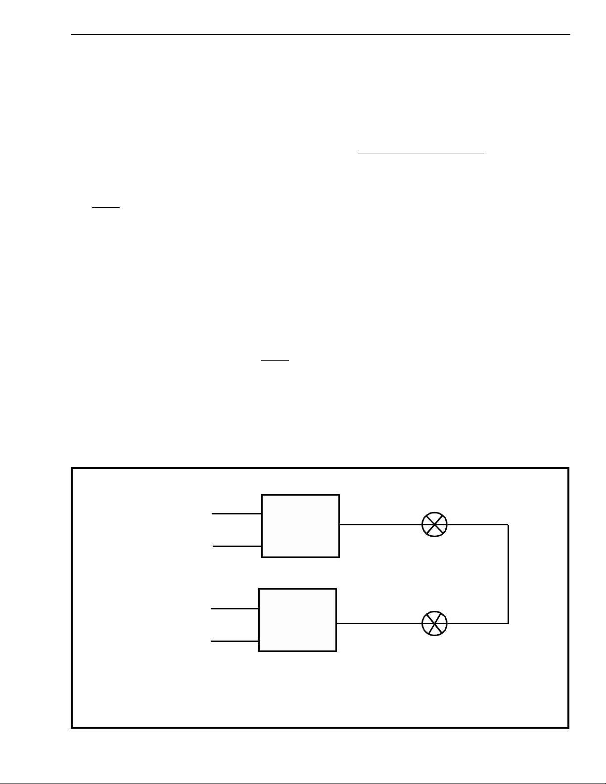
line. Figure 3 illustrates a typical connection between
two SLIC’s through two crosspoint switches. This
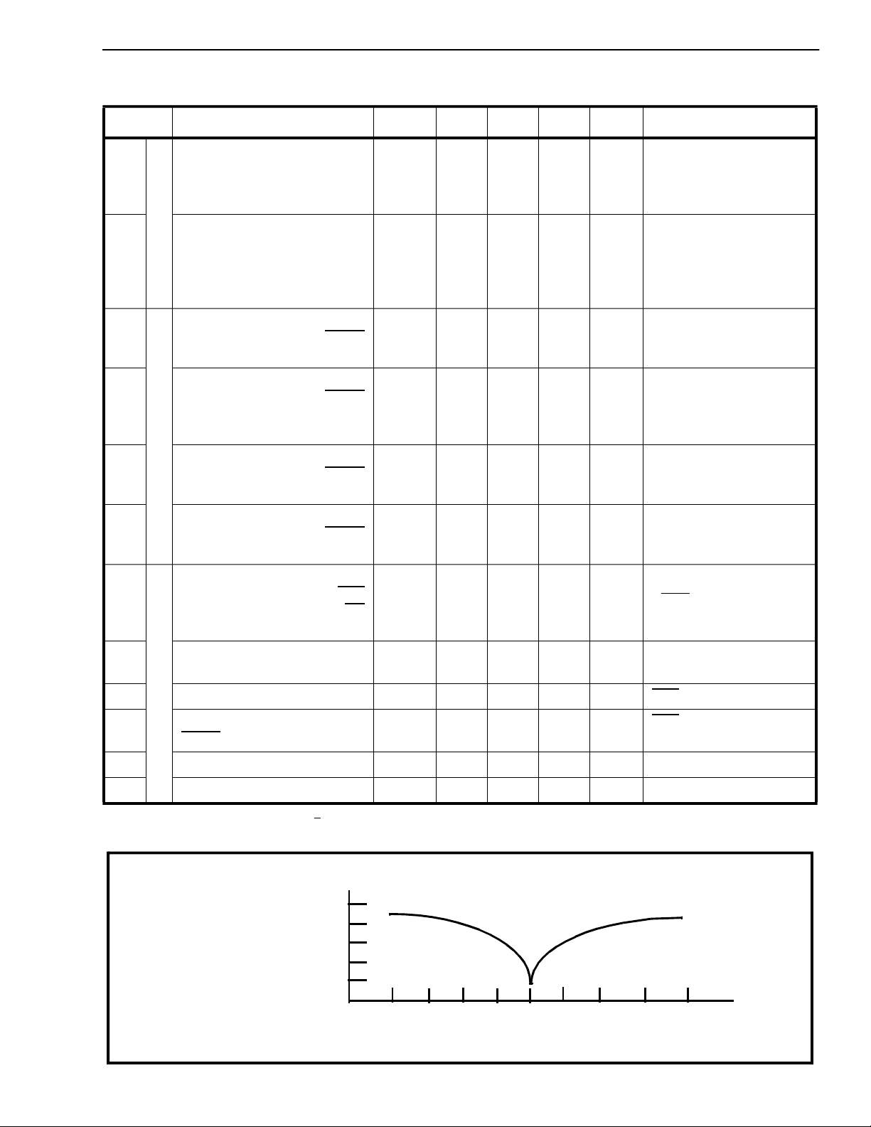
configuration gives optimum transhybrid loss as
seen from Figure 4 given that the output impedance
of the Junctor line is 604Ω.
The MUTE
input mutes signals coming from TIP and
RING to the junctor line while allowing the signal
from the jun c to r to the tip-rin g p air to b e tr an s m itte d .
Loop Detection
The loop detection circuit determines whether a low
enough impedances is across TIP and RING to be
recognized as an off-hook condition.
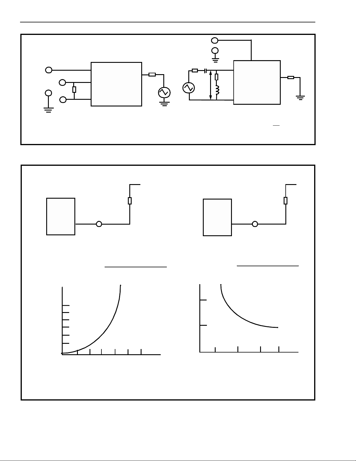
(Threshold impedance = 5.4kΩ with no adjustment)
This threshold level can be adjusted by the use of
external res istors as show n in Figure 6 . OFHK
low output drive capability so it may drive CMOS
operating with differe nt power supp lies.
has
Line Feed/Ring Feed Circuit
The line feed circuit provides loop current and the
ability to apply ringing onto TIP and RING. The
impedance from Ring Feed to GND is 600Ω which
gives the loop current as:
IL = Voltage at RING FEE D pin
Amps
Telephone Imp eda nce + 60 0
The positive supply for the line feed circuit is V
A1
through the loop current is determined from RING
FEED and GND.
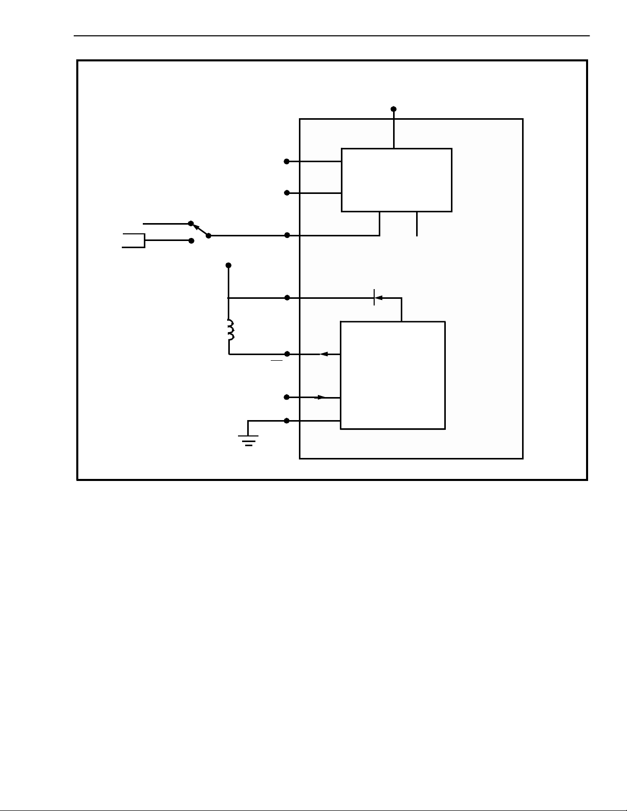
Relay Drive Circuit
The relay drive circuit switches ringing onto RING
FEED (Fig.7). The diode is present to suppress
voltage transients duri ng relay swi tches caused by
the inductive coils of the relay. Ringing voltage
includes AC ringing (90V typically) an dDC line
feed voltage (- 24V t ypical ly).
TIP
RING
TIP
RING
MH88500
1
TIP
JUNC
3
RING
16
75Ω
CROSSPOINT
SWITCH
MH88500
1
TIP
3
RING
JUNC
16
75Ω
CROSSPOINT
SWITC H
Figure 3 - SLIC Crosspoi nt S witc h Connecti on
2-35
Page 4

MH88500 Preliminary Information
Absolute Maximum Ratings†
Parameter Symbol Min Max Units
1 Voltage Supplies - V
2 Clamp Diode Breakdown Voltage-V
3 Operating Temperature T
4 Storage Temperature T
5 Power Dissipation P
† Exceeding these values may cause permanent dama ge. Functi on al operati on under these co ndition s is not implie d.
to GND V
Ref
to RGN D V
Ref
A1, VA2
V
C1
V
, V
CD
AMB
STG
B
C2
-18 +18 V
-35 V
0+70°C
-40 +100 °C
D
AC Electrical Characteristics†
Voltages are with respect to ground (VSS), TA = 25°C, unless otherwise stated .
Test conditions unless noted, VA1=VA2=+7V, VB=8V, VC2=-24V(+5%).
Characteristics Sym Min Typ
1 Junctor to differential output (tip-
ring) gain.
2 Differential Inp ut (tip -ring) to junct or
gain
A
JL
A
LJ
2.18 2. 2572.32 V/ VdB1kHz, 400mV
0.303 0 .321 0.321 V/ VdB1kHz, 1V
‡
Max Units Test Conditions
source on pin 16.
Note 2
Source on pins 1&3.
Note 1,2
+15 V
RMS
Watt
RMS
1.2
V
3 On/Off Hook Detection
Threshold
Loop Resist
Loop Current
R
Thresh
I
Thresh
4.0
3.6
5.4
4.0
6.0
5.3
kΩmANote 1.
Note 1
4 Trans Hybrid Loss 55 dB Notes 1,2. See
Figure 2
5 Passband Linearity +
6 Power Supply Rejection Rati o
PSRR 40 dB
1
dB Notes 1,2
Notes 1,2
(VC to Junctor)
7 Common Mode Rejection Ratio
CMRR 40 dB
Notes 1,2
(Tip and Ring to Junctor)
8 Low Frequency Cutoff (3dB )
Junctor to Line
Line to Junctor
F
LLJ
F
LJL
53
20
Hz
Hz
Notes 1,2
Notes 1,2
9 High Frequency Cutoff (3dB)
Line to Junctor
Junctor to Line
F
F
HLJ
HJL
800
500
10 Longitudinal Balan ce 65 dB
11 Tip (or Ring) to ground AC input
Z
I
300 Ω
kHz
kHz
Notes 1,2
Notes 1,2
Note 1
impedance
12 Junctor output impedance Z
† Exceeding these values may cause permanent dama ge. Functi on al operati on under these co ndition s is not implie d.
‡ Typical figures are at 25°C with nominal+
Note 1: 754Ω connected between JUNCTOR (pin 16) and OV.
Note 2: 604Ω connected between TIP (pin 1) and RING (pin 3).
2-36
5V supplies and are for design aid only: not guaranteed and not subject to production testing.
OJ
604 Ω
Page 5
Preliminary Information MH88500
DC Electrical Characteristics
.
Characteristics Sym Min Typ
1
2 Operating Supply Currents
3
Operating Supply Voltages
S
U
P
P
L
Y
High Level Input Voltage
VA1,V
V
VC1,V
MUTE
RC
4 Low Level Input Voltage
I
N
P
U
T
5 High Level Input Current
S
MUTE
RC
MUTE
RC
6 Low Level input Curren t
MUTE
RC
7
Sink Current
LED
RD
O
8 Diode Clamp Current I
U
T
P
9 High Level Output Voltage V
U
T
10 Low Level Output Voltage
S
OFHK
B
I
I
I
I
V
V
V
V
I
I
I
I
I
LED
I
RLY
V
A1
A2
I
C1
C2
IH
IH
IL
IL
RD
OH
OL
‡
Max Units Test Conditions
A2
A2
-13
-30
+13
-24
V
V
V
-20
7
8
B
6
.2
.1
mA
mA
mA
mA
mA
V
IH
IH
IL
IL
4.2
3
.8
1
-28
700
100
1
2
65
6
100
V
V
µA
µA
µA
µA
mAmAV
, -6V
OFHK
CD=RC=5V,RGD=0V
<1.5V
V
RRD
65 100 mA RC=RGND=0V,
CD=5V V
RRD
<1.5V
6 V LED Unconnected
-6.5 V LED Unconnected
11 High Level Out put Cur rent I
12 Low Level Out put Current I
‡ Typical figures are at 25°C with nominal+ 5V supplies and are for design aid only: not guaranteed and not subject to production testing.
TRANSHYBRID
LOSS
(dB)
10
20
30
40
50
60
OH
OL
550
10 µA
10 µΑ
850 900
600 650
LOAD IMPEDANCE ON JUNCTOR (Ω)
700 750
800
950
Figure 4 - Return Loss VS Junctor Lo ad I mped ance
2-37
Page 6
MH88500 Preliminary Information
VO
VTR
VTR
R and R
MH88500
5
1
MH88500
604Ω
CAN BE MEASURED THAT
V
3
=2VX=2V
TP
TR
(a)
Figure 5 - Transhybr id Loss Test Circuit
THRESH
(a)
(kΩ)
11
THRESH
ADJ
16
GND
754Ω
VX
604Ω
10µF
1
200Ω
VS
10H
MH88500
3
TRANSHYBRID LOSS = - 20LOG (VO
(b) 2VS
R and R
THRESH
(a)
MH88500
11
THRESH
5
ADJ
16
(kΩ)
54Ω
)
VC2
RR
R
120
100
80
60
40
20
R =
(48 x R
5.4 - R
THRESH
THRESH
) -28.8
(912 x R
R =
R
R
THRESH
THRESH
) +604
- 5.4
(kΩ)(kΩ)
2000
1000
1
3
2
456
R
THRESH
(kΩ)
10
20
(a)
30 40
R
THRESH
(b)
(kΩ)
Figure 6 - Off-Hook Threshold Ad just
2-38
Page 7
Preliminary Information MH88500
V
A1
TIP
LINE FEED/
RING FEED
MH88500
CLAMP DIODE
-24VD C
+90VAC
RING
-24VD C
RING FEED
+V
CD
RELAY COIL
RD
RELAY
CIRCUIT
RC
RGND
Figure 7 - Relay Drive Cir cui t
DRIVE
2-39
Page 8
MH88500 Preliminary Information
CONTROL
LOGIC
ADDRESS
OUT
A
L
0-A2/D0-D3
MT8812
Crosspoint
Switch
0
A0
A1
A2
MD74SC137
1 OF 8
DECODER
A0
A1
A2
MD74SC137
1 OF 8
DECODER
J
0
J
1
J
2
J
3
-L
7
00
01
02
03
04
05
06
07
00
01
02
03
04
05
06
07
5 MORE
SLICS
5 MORE
SLICS
+7v +5V
2 12 9 20 17 4
15
19
MH88 500
10
-8V -24V 0V
+5V
+7V
2
15
MH88500
19
10
+7V +5V +5V
15
19
10
86147
16
-8V
-24V
MH88500
16 8
+5V
TIP
RING
7146816
+5V
1720912
4
TIP
RING
0V
4
17209122
TIP
RING
6147
-24VDC
90VAC
-24VDC
1
3
-24VDC
90VAC
-24VDC
1
3
-24VDC
90VAC
-24VDC
1
3
2-40
CMOS
A0
A1
8-INPUT
A2
SELECT
OUTPUT
4512
MUX
D
0
D
1
D
2
|
|
D
7
-8V
-24V
0V
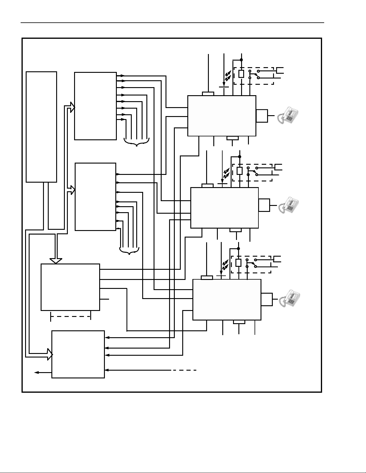
Figure 8 - PABX Typical Applicatio n
Page 9
Preliminary Information MH88500
Side View
0.010 +
(0.25 +
Notes:
1) Not to scale
2)Dimensions in inches).
3) (Dimen sions in millimet res).
*Dimensio ns to centre of pin &
tolerance non ac cumulati ve.
0.080 Max
(2.0 Max)
0.002
0.05)
0.12 Max
(3.1 Max)
0.02
0.52+
(13.2+
0.05 +
(1.3 +
0.5)
0.01
0.5)
1234 1920
***
0.05 +
0.02
(1.3 +
0.05)
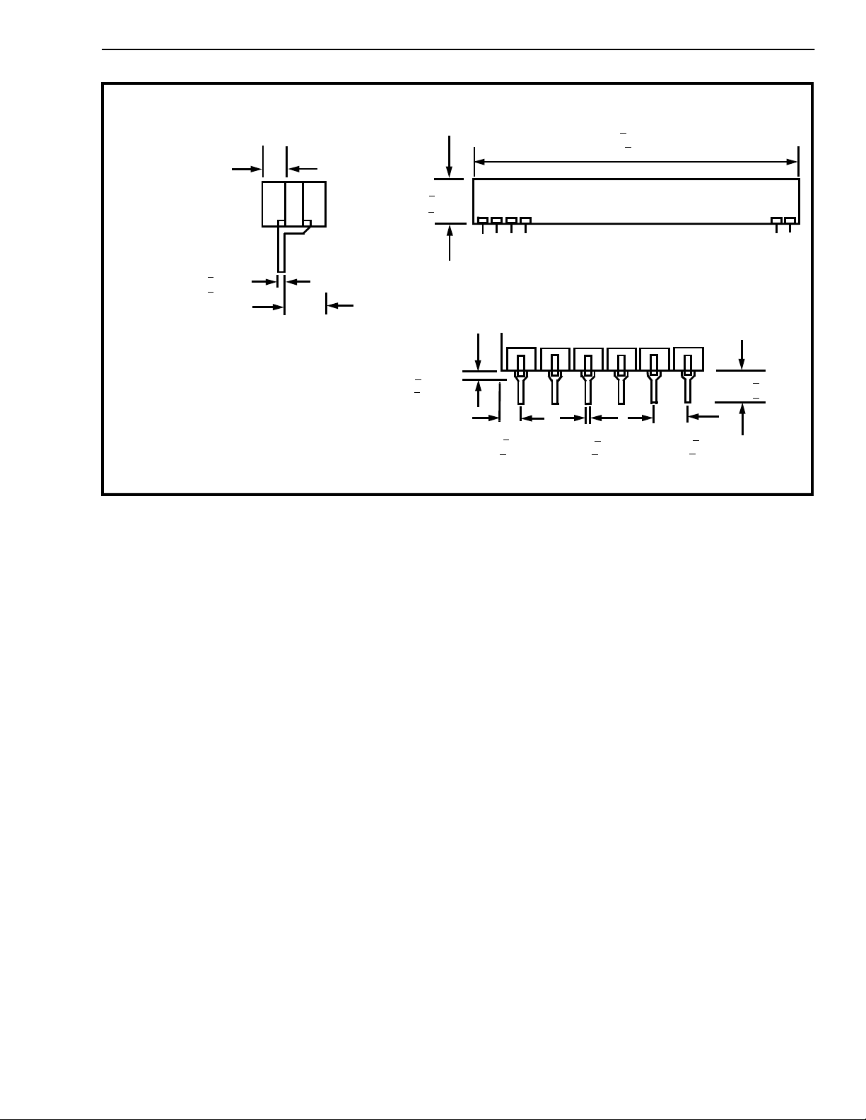
Figure 9 -Mechanical Data
0.02 0 +
(0.51 +
2.00 + 0.02 0
0.5)
(50.8 +
0.05
0.13)
0.100 +
(2.54 +
0.10
0.13)
0.18 +
(4.6 +
0.02
0.5)
2-41
Page 10

MH88500 Preliminary Information
Notes:
2-42
 Loading...