

Page 1
MH88422
Line Interface Circuit
Preliminary Information
Features
• FAX and Modem interf ace (V29/V2 2 bis)
• Variants mat ch Germ an, UK & 600
Ω network
impedance s
• Provides reinforced barrier to interna tional PTT
requiremen ts
• Transformerless 2-4 W ire conversion
• Loop star t oper ation
• Pulse and DT MF operati on
• Accommo date s extern al mo nitor ph one
• Line state dete ction out put s:
• -l oop curr ent/ri nging outp uts
• Single +5V operat ion, l ow idle po wer (5 mW)
• Full Duplex
• Suitable for p ower dow n ap plica tions
Applications
Interface to Central Office for:
•DAA
• Modem
•FAX
• Answering M achi ne
• Terminal Equip men t
ISSUE 5 April 1995
Ordering Information
MH88422 -1 14 Pin DIL Pa ckage
MH88422 -2 14 Pin DIL Packag e
MH88422 -3 14 Pin DIL Packag e
Surface Mount Options are available by adding the
Suffix “S”
Description
The Mitel MH88422 Line Interface Circuit provides a
complete audio and signalling link between audio
equipment and central office. The functions provided
by the MH88422 include 2-4 Wire conversion, loop
seizure, ring voltage and loop current detection. The
device is fabricated as thick film hybrid which
incorporates various technologies for optimum circuit
design, high voltage isolation and very high
reliability.
Variants are provided to meet German (-1) and UK
(-3) line impedance (see section on Line
Impedances), as well as a 600Ω variants (-2).
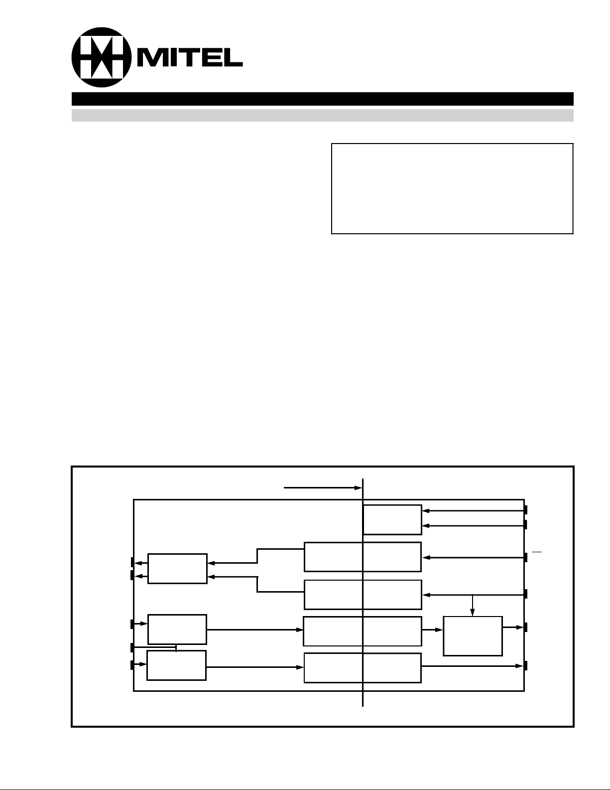
Isolation Barrier
Power
Supply
Opto-
TIP
RING
Active
Termina tio n
TXIN
TF
RLS
Audio Input
Buffer
Input
Buffer
NETWORK CONNECTIONS
Isolation
Opto-
Isolation
Opto-
Isolation
Opto-
Isolation
Logic Input
Buffer
Audio
Buffer
Audio
Buffer
Loop
Ring &
Buffer
USER CONNECTIONS
Transhybrid
Loss
Cancellat io n
Circuit
VDD
AGND
LC
VR
VX
RVLC
Figure 1 - Functional Block Diagram
2-21
Page 2
MH88422 Preliminary Information
VDD
AGND
LC
RVLC
NC
VX
VR
1
2
3
4
5
6
78
14
TIP
13
RLS
12
NC
11
TF
10
TXIN
RING
9
NC
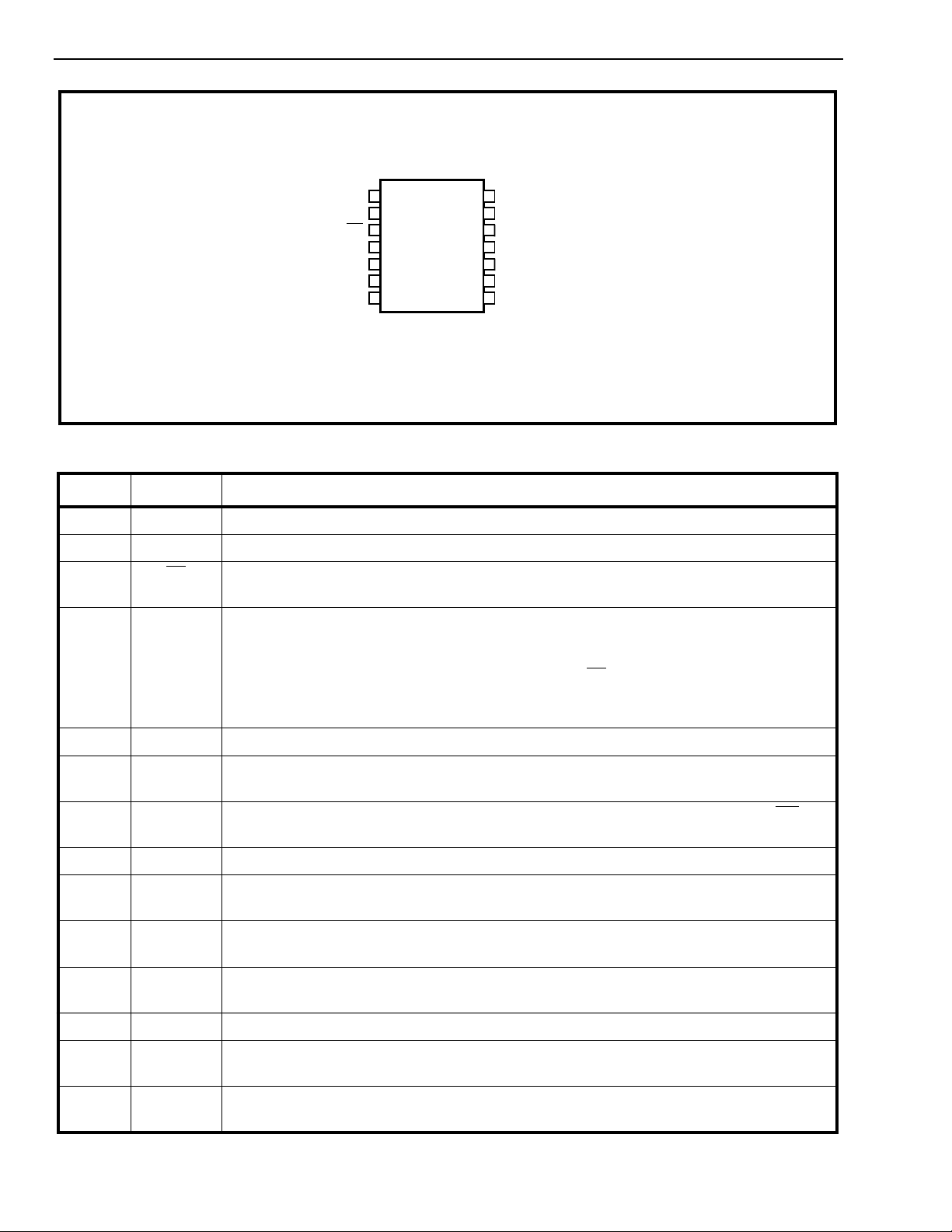
Figure 2 - Pin Connections
Pin Description
Pin # Name Description
1VDDPositive Pow er Su pp ly Voltage. +5V.
2AGNDAnalog Ground. 4-Wire Ground. Normally connect ed to System Ground.
3LC
4RVLCRin g Voltage and Current Detect (Output). A logic low indicates that loop current is
Loop Control (Input). A logic low activates internal circuitr y which provides a dc
termination across Tip and Ring. Used for seizing the line and dial pulsing.
detected. The loop current can be due to the external monitor phone or the MH88422 in
the off-hook mode. The RVLC output pulses when the external monitor phone is dial
pulsing or when the MH88422 is dial pulsing via the LC
input. In addition, when the
MH88422 is on the on-hook mode, a pulsing output indicates ringing voltage across the
Tip and Ring leads. The pulsing output frequency is twice the ringing frequency.
5NCNo Connection should be mad e to this pin.
6VXTransmit (Outp u t). 4-Wire ground (AGND) referenced audio out put , biased at 2.5V.
Outputs in off-hook mode only.
7VRRecei ve (In pu t). 4-Wire ground (AG ND) referenced audio input, biased at 2.5V. LC
must be activated low and loop current must be flowing .
8NCNo Connection should be mad e to this pin.
9 RING Ring Lead. Connects to the “Ring” lead of the central office through an opt iona l relay
contact. The central office “Tip” and “Ring” leads may be interchanged.
10 TXIN Transmit (Input). Connects to the “Ring” lead of the central offi ce through a coupli ng
capacitor.
11 TF Tip Feed. Connects to the “Tip” lead of the central office through an internal resistor and
an optional external resistor.
12 NC No Connection sho uld be mad e to this pin.
13 RLS Ring Loop Sense (Input). Sense node for ringing voltage detector and the loop current
detector.
14 TIP Tip Lead. Connects to the “Tip” lead of the central office through an opti onal relay
contact. The central office “Tip” and “Ring” leads may be interchanged.
2-22
Page 3

Preliminary Information MH88422
Functional Description
The MH88422 Line Interface Circuit is a COIC
(Central Office Interface Circuit) used to interface
FAX’s Modems or user defined equipment to Central
Office 2-Wire Analog Trunks.
Opto-Isolation
The isolation barrier is designed to meet regulatory
requirements for a reinforced barrier of 3kVac. It
provides full isolation of mains voltages up to 250V
RMS and all telecom voltages.
In order that this barrier is not bypassed a creepage/
clearance distance of 6.4mm minimum must be
maintained between wiring, pcb tracking, etc.,
connected to external circuitry on either side of the
barrier. To make this requirement simpler, pins on the
MH88422 connected to opposite sides of the barrier
are on opposite sides of the package.
External Protection Circuit
The RVLC outputs pulses when the external monitor
phone is dial pulsing or when the MH88422 is dial
pulsing via the LC
In addition, when the MH88422 is on-hook, a pulsing
output indicates that ringing voltage is across the tip
and ring leads; the pulsing output frequency is twice
the ringing frequency. See Figure 3.
Ringing frequency may require external validation.
An RC monostable is usually satisfactory for this
purpose or this may also be achieved using software
applications.
mode.
2-4 Wire Conversion
The 2-4 Wire conversion circuit converts the
balanced full duplex signal at Tip and Ring of the
central office line into a transmit ground referenced
signal at VX (Transmit) of the MH88422. It also
converts the receive ground referenced signal at VR
(Receive) of the MH88422 into a balanced transmit
signal at Tip and Ring of the central office line.
To meet regulatory high voltage requirement, an
external protection circuit is required. The protection
circuit shown in Figure 3 (Clamp Diode D1) is
recommended.
DC Loop Termination
The DC loop termination circuitry provides the loop
with an active DC load termination when a logic low
is applied to the LC
termination is similar to a resistance of
approximately 300Ω (loop current dependent).
Internal optically isolated circuitry is used to switch
the termination in and out the loop. This is used for
both seizing the line as well as generating dial
pulses. The MH88422 will not seize the line when
powered down.
(Loop Control) input. The
Supervision Features
The supervision circuitry is capable of detecting
ringing voltage and loop current as well as the status
of an optional external monitor phone. The RVLC
(Ring Voltage Loop Current Detect) output provides
a logic low when loop current flows due to the
external monitor phone or the MH88422 being in the
off-hook m ode .
In full duplex transmission, the Tip-Ring signal
consists of an audio signal from the central office as
well as an audio signal due to the VR input. There is
an internal cancellation circuit which prevents the V
signal appearing at the VX output. The degree to
which the 2-4 wire conver sion circuit min imizes the
contribution of the VR signal at the VX output is
specified as transhybrid loss (THL).
The MH88422 is suitable to drive a COMBO II codec
or a VLSI modem device.
Line Impedance
The MH88422 provides a fixed Tip-ring impedance
which conforms to the following PTT requirements.
MH88422-1 Zin = 200 + 820 // 115nF
Germany
MH88422-2 Zin = 600Ω
MH88422-3 Zin = 370 + 620 // 310nF
UK
R
2-23
Page 4
MH88422 Preliminary Information
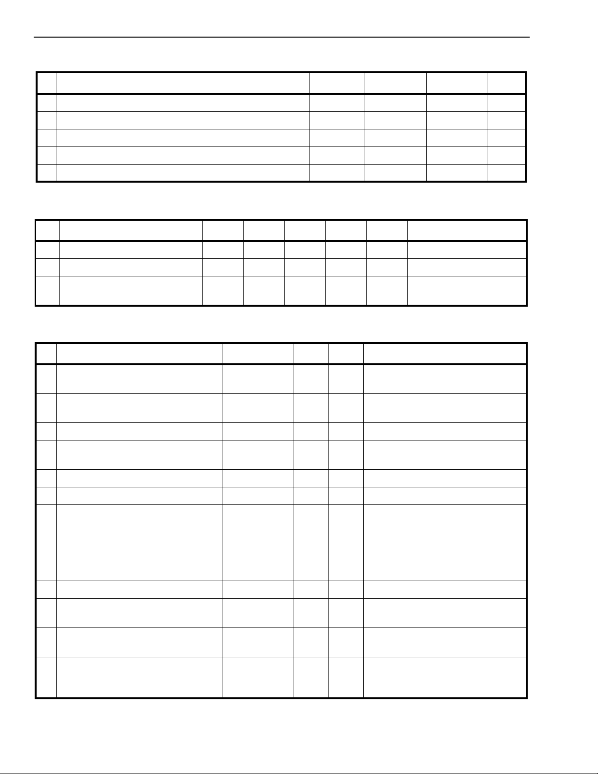
Absolute Maximum Ratings* - All voltages are with respect to AGND unless otherwise specified.
Parameter Symbol Min Max Units
.
1 DC Supply Voltage V
2 Storage Temperature T
3 DC Loop Voltage V
4 Ringing Voltage V
5 Loop Current I
* Exceeding these values may cause permanent damage. Functional operation under these conditions is not implied
DD
S
Bat
R
Loop
Recommended Operating Conditions.
Parameters Sym Min Typ
1 DC Supply Voltages V
2 Operating Temperature T
3 Ringing Voltage V
‡ Typical figures are at 25°C with nom inal +5V sup ply and are for design aid only
DD
OP
R
4.5 5.0 5.5 V
070°C
‡
Max Units Test Conditions
75 V
Loop Electrical Characteristics*
‡
Characteristics Sym Min Typ
1
Ringing Voltage No Detect
-1 Variant only Detect
Ringing Voltage No Detect
All other Variants Detect
2
Ringing Frequency 15 68 Hz
VR
27
VR
14
Max Units Test Conditions
20 V
7V
V
V
RMS
RMS
RMS
RMS
-0.3 6 V
-55 +80 °C
-100 +100 V
- 120 V
-90
V
RMS
Bat
=-48V
Refer to FT2 1TR2 for test
method
Externally
Adjustable
RMS
mA
3
On-Hook 2-wire Impedance 40k Ω 1kHz
4
Operating Loop Current 15 80 mA
5
Operating Loop Resista nce 2800 Ω V
6
Off-Hook DC -1 Variant
Voltage
-2 Variant
-3 Variant
7
Leakage Current (2-Wire to AGND) 10 µ A 100V
8
Leakage Current on Hook
6.0
6.0
4.0
4.0
6.0
6.0
9.6
15
6.0
7.8
9.0
12.5
V
V
V
V
V
V
910µAV
(Tip to Ring)
9
DC Resistance during dialling
-1 variant only 200 220 Ω I
10
Dial Pulse Distort ion ON
-1 Variant OFF
All other Variant
* Loop Electrical Characteristics are over recommended operating conditions unless otherwise stated.
‡ Typical figures are at 25°C and are for desi gn aid only.
Note 1: All of the above characteristics use a test circuit as per Figure 3.
0
+6
0
+2
+8
+2
+4
+10
+4
ms
ms
ms
=-48V, I
Bat
=25mA
I
Loop
=42mA
I
Loop
=15-20mA
I
Loop
=26mA
I
Loop
=25mA
I
Loop
=42mA
I
Loop
=-50V
Bat
=20-40mA
Loop
DC
Loop
=15mA
2-24
Page 5
Preliminary Information MH88422
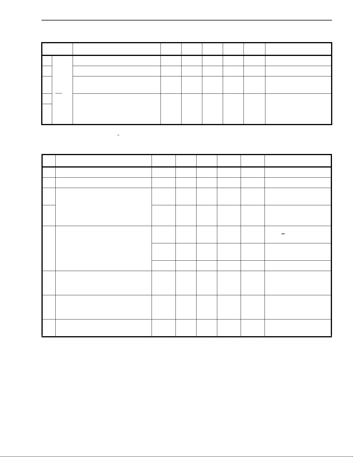
DC Electrical Characteristics†
Characteristics Sym Min Typ
‡
Max Units Test Conditions
1
2 Power Consumption PC 15 mW V
3 Low Level Output Voltage
RVLC
LC
4 Low Level Input Voltage
5
† DC Electrical Characteristics are over Recommended Operating Conditions unless otherwise stated.
‡ Typical figures are at 25°C with nominal+
Supply Current I
High Level Output Voltage
High Level Input Voltage
Low Level Input Current
High Level Input Current
5V supplies and are for design aid only.
DD
V
OL
V
OH
V
V
I
IH
I
IL
2.4
IL
2.0
IH
3mAV
0.4 V
V
0.8
V
V
60
µΑµAV
60
= -5.0V, Idle state
DD
= -5.0V, Idle state
DD
I
= 4mA
OL
= 0.4mA
I
OH
= 5.0V
IH
= 0.0V
V
IL
AC Electrical Characteristics† - MH88422 All Variants
Characteristi cs Sym Min Typ
1 Input Impedance VR 47k Ω
2 Output Impedance at VX
3 Receive Gain (VR to 2-wire)
40
Frequency Response Gain
(relative to Gain @ 1kHz)
‡
Max Units Test Conditions
10 Ω
3.5 dB Input 0.5V at 1kHz
dB
0
dB
300 Hz
3400 Hz
5 Signal Output Overload Level
at 2-Wire
6 Total Harmonic Distortion
at 2-wire
7 Power Supply Reject Ratio
at 2-wire
at VX
at VX
at VX
+2.0 +3.0 dBm V
+2.0 +3.0 dBm
THD
PSRR
1.2
1.2
30
30
%
%
dB
dB
5% @ 1kHz
THD <
=15 to 40mA
I
Loop
=4.5V to 5.5V
DD
Input -10dB at 1 kHz
DC loop = 25mA
=5.0V
V
DD
Ripple 0.1V,1kHz on
V
DD
8 Transhybrid Loss THL 20 dB Input -3.5dBm, 1kHz at
V
R
† Electrical Characteristics are over Recommended Operating Conditions unless otherwise stated.
‡ Typical figures are at 25°C and are for design aid only.
Note 1: All of the above characteristics use a test circuit as per Figure 3.
Note 2: All of the above test conditions use a test source impedance which matches the device’s impedance.
Note 3: dBm is referenced to 600Ω unless otherwise stated.
2-25
Page 6
MH88422 Preliminary Information
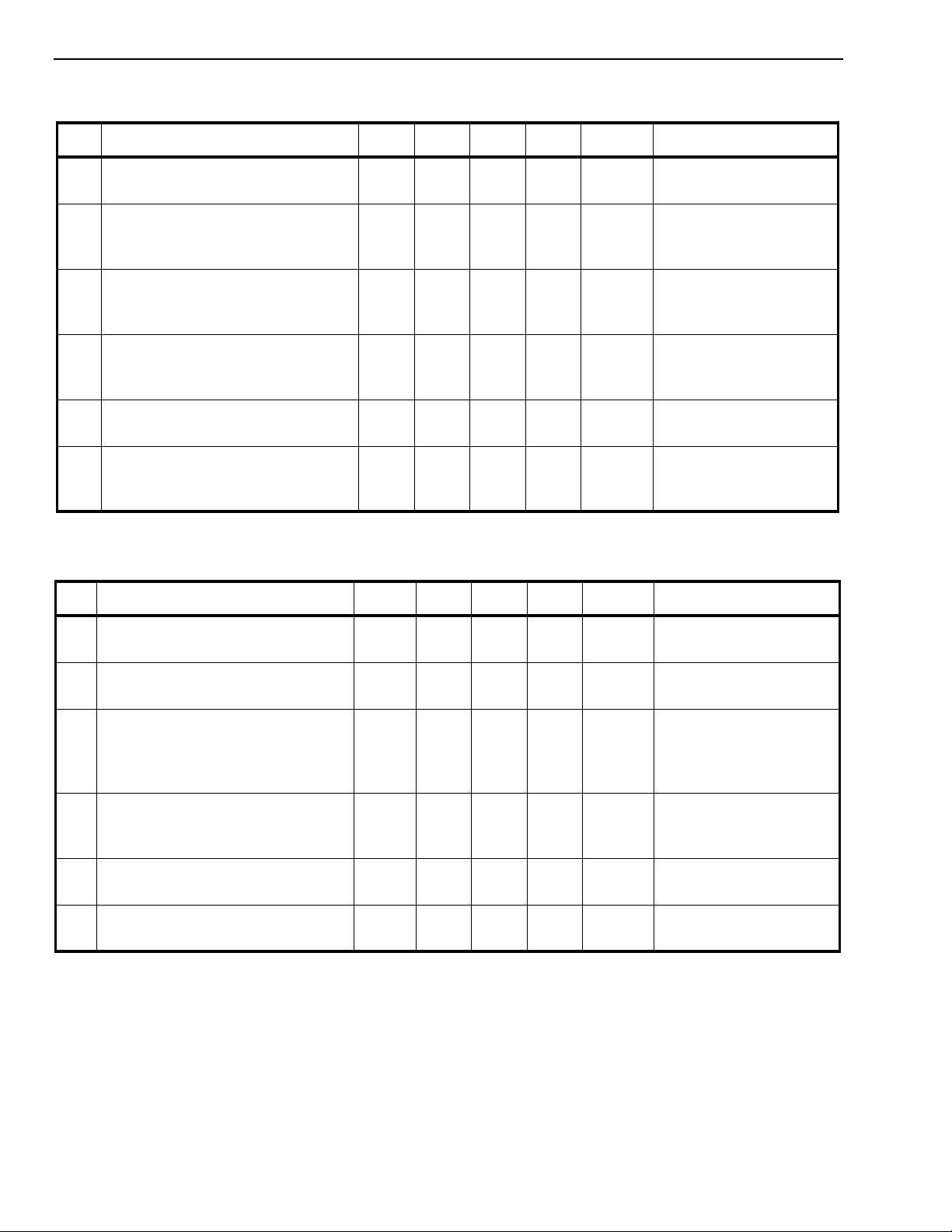
AC Electrical Characteristics† - MH88422-1
Characteris tics Sym M in Typ
‡
Max Units Test Conditions
1 2-Wire input Impedance
Zin 900 Ω @ 1kHz
(200Ω + 8 20 Ω //115nF)
2 Retu rn Loss at 2-Wire
(200Ω + 8 20 Ω //115nF)
3 Longit udi nal to Meta llic Ba lance 40
4 Idle Channel Noise
at 2-Wire
At VX
RL 20
20
20
55
53
Nc
22
24
26
65
60
60
-72
-72
dB
dB
dB
dB
dB
dB
-58 dBmp
dBmp
300-500Hz
500-2500Hz
2500-3400Hz
50-300Hz
300-1000Hz
1000-4000Hz
5 Transmit Gain (2-Wire to VX) -0.4 dB Input 0.5V @ 1kHz
Off -Hook
6 Frequen cy Response Gain
(relative to gain @ 1kHz)
† Electrical Characteristics are over Recommended Operating Conditions unless otherwise stated.
‡ Typical figures are at 25°C and are for design aid only.
-0.6
-0.6
dB
dB
300Hz
3400Hz
AC Electrical Characteristics† - MH88422-2
‡
Characteristi cs Sym Min Typ
Max Units Test Conditions
1 2-Wire Input Impedance
ZIn 600 Ω @ 1kHz
(600Ω)
2 Return Loss at 2-Wire
(Reference 600Ω )
3 Longitudinal to Metallic Balance
Metallic to Longitudinal Balance
4 Idle Channel Noise
at 2-Wire
at VX
ERL
SFRL2014
58
53
60
40
Nc
20
18
60
55
13
13
dB 500-2500Hz
dB
dB
dB
dB
20 dBrnC
dBrnC
200-3200Hz
200-1000Hz
1k-3kHz
200-1000Hz
1k-4kHz
5 Transmit Gain (2-Wire to Vx) -0.4 dB Input 0.5V @ 1kHz
Off- Hook
6 Frequency Response Gain
(relative to gain @ 1kHz)
† Electrical Characteristics are over Recommended Operating Conditions unless otherwise stated.
‡ Typical figures are at 25°C and are for design aid only.
-0.6
-0.6
dB
dB
200Hz
3400Hz
2-26
Page 7

Preliminary Information MH89770
AC Electrical Characteristics† - MH88422-3
Characteristics Sym Min Typ‡Max Units Test Conditions
1 2-Wire In put I mpe dance
(370Ω + 6 20 Ω // 310nF)
2 Retu rn Loss at 2-Wire
(370Ω + 6 20 Ω // 310nF)
3 Longit udi nal to Meta llic Balance 50 60 dB 300-3400Hz
4 Idle Channel Noise
at 2-Wire
at VX
5 Transmit Gain (2-Wire to Vx) -0.4 dB Input 0.5V @ 1kHz
6 Freque n cy Gain
(relative to gain @ 1kHz)
† AC Electrical Characteristics are over Recommended Operating Conditions unless otherwise stated.
‡ Typical figures are at 25°C and are for design aid only.
Note 1: All of the above characteristics use a test circuit as per Figure 3.
Note 2: All of the above test conditions use a test source impedance which matches the device’s impedance.
Note 3: dBm is referenced to 600Ω unless otherwise stated.
TIP-RING Drive Circuit
The audio input ground (AGND) referenced signal at
VR, biased at 2.5V, is converted to a balanced output
signal at Tip-Ring. 2-4 wire isolation is achieved
through the use of optocouplers when the LC
activated, low, and loop current flowing.
Zin 700 Ω @ 1kHz
RL 18 20 dB 200-2400Hz
Nc
-80
-80
-0.6
-0.6
The output impedance of the VX output is about 10Ω,
therefore, with two external 1kΩ resistors configured
as per Figure 5, this will result in 6dB of attenuation fo r
a total gain of -6.4dB. For cor rec t gai n, t he M H8 842 2
input impedance must match the line impedance.
input is
-70
-68
dBmp
dBmp
dB
dB
Off-Hook
300Hz
3400Hz
Receive G ain
TIP-RING Receive Circuit
The differential audio signal at Tip-Ring is converted to
a ground (AGND) referenced si gnal, bia sed at 2. 5V, at
the VX output. 2-4 Wire isolat ion is achieved through
the use of o ptocouplers. The receive circuit operated
when LC
is low and loop current is flowing
Transmit Ga in
Transmit Gain (Tip-Ring to VX) is fixed as indicat ed in
“AC Electrical Characteristics”.
However, by adding external resistors to the VX
output, the Transmit Gain can be reduced as shown in
Figure 5. To limit the output current drawn, the
minimum recomm ended resista nce to ground is 2kΩ.
Overall Transmit Gain =
-0.4 dB + 20log (R4 / (R4 + R3))
Receive Gain (VR to Tip-Ring) is fixed as indicated in
“AC Electrical Cha ra c te ristics”. Howeve r, by adding a
single external resistor in series with the VR input,
the Receive Gain can be reduced.
Overall Receive Gain =
3.5dB + 20log (47kΩ /(47kΩ + Rext),
The input impedance of the VR input is 47kΩ,
therefore, an external 100kΩ resistor in series with
this input will result in 10dB of attenuation for a total
gain of - 6. 5d B.
For correct gain, the MH88422 input impedance
must match the line impedance.
2-27
Page 8
MH88422 Preliminary Information
TIP
D1
RING
NOTES:
Calls are set up and cleared in this mode by the
external controller. It turns on the loop via Loop
Control, diallin g by pulsing loop control (or via
DTMF tones) and clearing down by turning Loop
Control off.
VX
VR
RVLC
LC
6
7
4
3
Ring Voltage & Loop
Current Detect Output
Loop Control Input
C2
14
13
11
10
MH88422
TIP
RLS
TF
TXIN
9
RING
1
+5V
AGNDVDD
2
+
C1
1) C1: 10µF, 6V Ta ntalum
2) C2: 0.1µF, 250V (Typical Value)
3) D1: 180VDC Foldback Diode, e.g. TISP4180, TISP5180
4) VX and VR are biased at 2.5V, therefore, coupling capacitors
may be required depending on application.
Audio Output
Audio Input
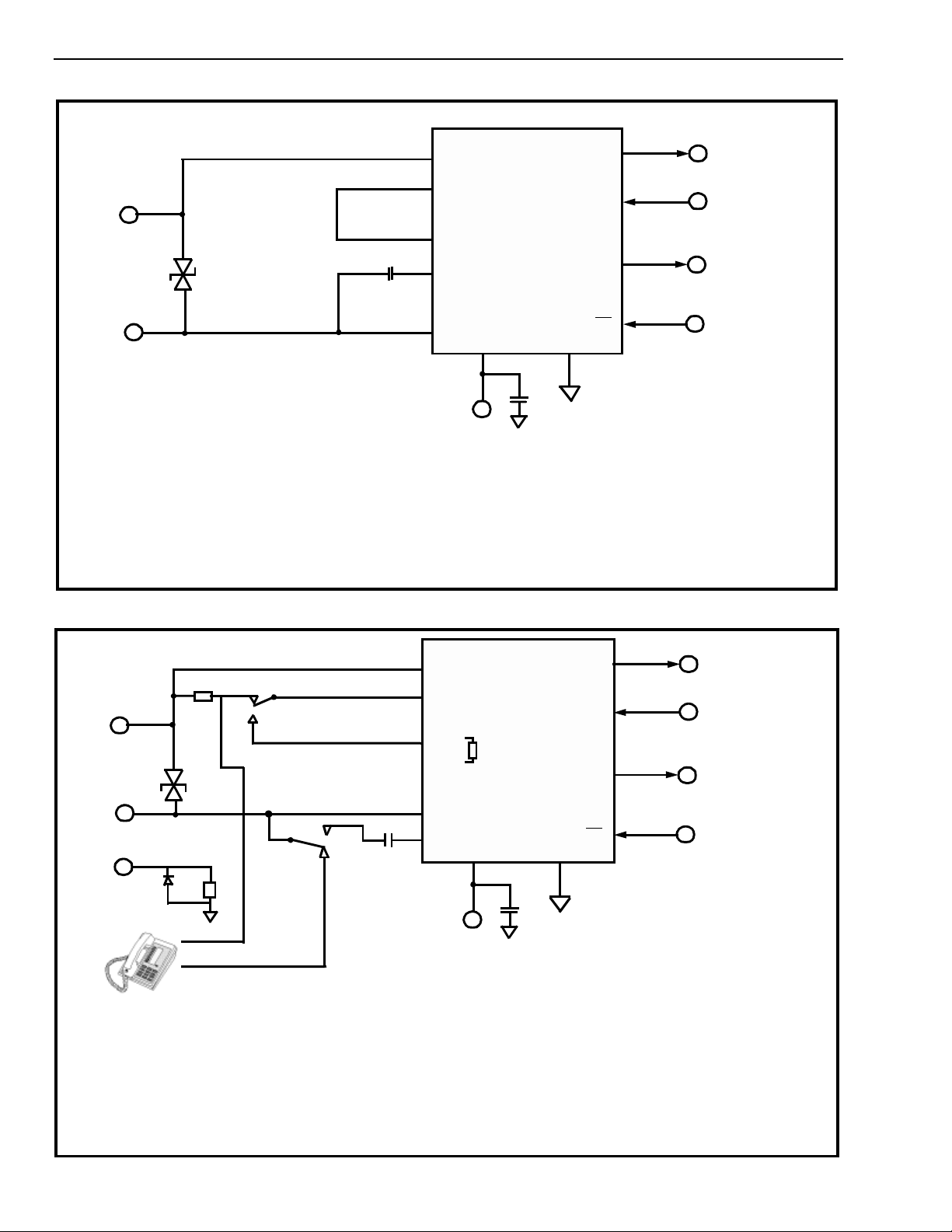
Figure 3 - Typical Applicati on Circuit
14
R6
TIP
D1
RING
Line
Relay
Input
NOTES:
R2 & C2 form a dummy ringer, where R2 is on the hybrid and C2 must be fitted by the customer.
To initate a manual call, lift the handset. The RVLC pin will indicat e that the line has been seize d by the monito r phone .
The required numbe r is then dialled and the connecti on s esta blishe d. Duri ng this phase the Loop Cont rol
input should be turned ON to ensure that when the relay K1 is operated and the monitor phone removed from the line loop
current is still maintained . On receipt of the corre ct progress tones the externa l control le r shoul d contro l the data tran smission
and clear down the call when it is comp let ed by turn in g the Loop Con trol OFF. For applicatio ns in som e coun trie s su ch as
Germany the MH88422 can not be used with an optional telephone but may still be used in a combined telephone/fax machine.
K1a
K1b
C2
K1
K1b
5) R6 adjust the monitor phone detect sensitivity typically set to 200 ohms for 5mA limit on the
-1 variant and 75 ohms on the -3 variant.
6) K1b is added to remove the dummy ringer when using a combined phone on the-1 variant
and is not required for all other variants.
13
11
10
9
TIP
RLS
TF
RING
TXIN
MH88422
R2
Internal
dummy
Ringer
Resistor
1
+5V
+
C1
3) D1: 180VDC Foldback Diode, e.g. TISP4180, TISP5180
4) VX and VR are biased at 2.5V, therefore , coup ling capa cito rs
may be required depe nd ing on ap plication.
RVLC
AGNDVDD
2
6
VX
7
VR
4
3
LC
1) C1: 10µF, 6V Tantalum
2) C2: 0.47µF, 100V
Ring Voltage & Loop
Current Detect Outpu t
Audio Output
Audio Input
Loop Control Input
2-28
Figure 4 - Typical Appl icati on Circu it wi th Dum my Ri ng er and M on ito r Phone
Page 9
Preliminary Information MH88422
TIP
D1
RING
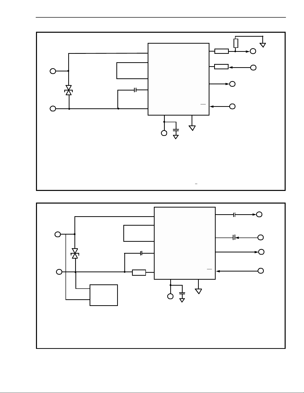
RECEIVE GAIN:
Audio input to Tip-Ring
=20log(47k/(R5+47K))+3.5dB
= -6.5dB
TRANSMIT GAIN:
Tip-Ring to Audio Output
=20log(R4(R3+ R4))- 0.4dB
= -6.4dB
Note:
The VX output gain has been reduced by 6dB
(to -6.4dB) and the VR input gain has been
reduced by 9.9dB (to -6.4dB) in this example.
C2
14
13
10
R3
TIP
MH88422
RLS
11
TF
RVLC
TXIN
9
RING
VDD
1
+5V
1) C1: 10µF, 6V Tantalum
2) C2: 0.1µF, 250V (Typical Value)
180VDC Foldback Diode, e.g. TISP 4180 , TISP5 180
3) D1:
4) VX and VR are biased at 2.5V, therefor e, coup ling capacito r s
may be required depending on application.
5) (R3+R4) should be > 2kΩ to prevent overload.
AGND
2
+
C1
VX
VR
LC
6
100k
7
R5
4
3
R4
Audio Output
Audio Input
Ring Voltage & Loop
Current Detect Output
Loop Control Input
Figure 5 - Typical App licati on Circuit for Gai n Adju stm ent
14
TIP
13
RLS
TIP
D1
RING
Meter
Pulse
Detector
Note:
Meter pulses at high frequency (16kHz or 12kHz) and high level (10V RMS) are used in some countries.
The VX amplifier has a low pass filter which attenuates by typically 15dB at 16kHz (For the -1 variant).
If this proves insufficient for specific applications, an LC reject filter is recommended.
C2
Meter
Pulse
Filter
11
10
TF
TXIN
9
RING
MH88422
1
+5V
VX
VR
RVLC
LC
AGNDVDD
2
+
C1
6
10µF
7
10µF
4
Current Detect Output
3
1) C1: 10µF, 6V Ta ntalum
2) C2: 0.1µF, 250V (Typical Value)
3) D1:180VDC Foldback Diode,
e.g. TISP4180, TISP5 18 0.
Audio Output
Audio Input
Ring Voltage & Loop
Loop Control Input
Figure 6 - Typical Application Circui t with Meter Pul se Filter and Coup ling Capaci t or
2-29
Page 10
MH88422 Preliminary Information
AAAA
AAAA
AAAA
AAAA
A
A
AAA
AAAA
AAAA
AAAA
AAAA
A
A
A
AAA
TIP
C2
D1
RING
Notes:
1) C1: 10µF, 6V Tantalum
2) C2:1.8µF, 250V (Normally in master socket)
3) D1:180VDC Foldback Diode , e.g. TISP418 0, TISP518 0
14
13
11
10
TIP
MH88422
RLS
TF
TXIN
9
RING
1
VDD
R2
RVLC
AGND
2
+
VX
VR
LC
6
7
4
Audio Output
Audio Input
Ring Voltage & Loop
Current Detect Output
3
Loop Control Input
C1
+5V
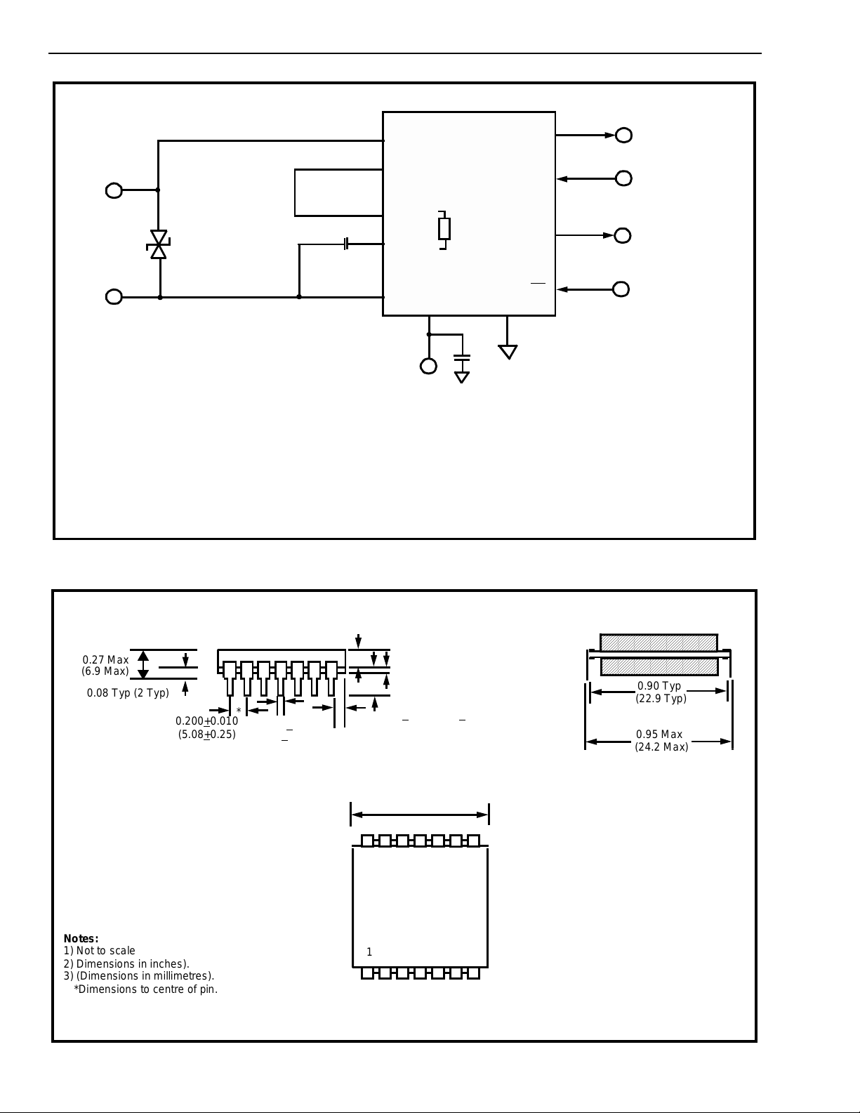
Figure 7 -Typical Application Circuit show in g UK Dumm y Ringe r Circu it.
0.27 Max
(6.9 Max)
0.08 Typ (2 Typ)
0.200+
(5.08+
Notes:
1) Not to sc ale
2) Dimensions in inches).
3) (Dimensions in millimetres).
*Dim en si on s to ce ntre of pin.
0.010
0.25)
*
0.19 Max (4.8 Max)
0.020 + 0.005
(0.5 +
0.12)
0.10 Typ
(2.54 Typ)
0.063 Max(1.6 Min)
0.015 (6.6+0.4)
0.26+
1.42 Max
(36.1 Max)
1
AAA
AAA
AAA
AAA
AAA
AAA
AAAA
AAAA
AAAA
AAAA
AAAA
AAAA
AAAA
AAAA
AAAA
AAAA
AAAA
AAAA
0.90 Typ
(22.9 Typ)
0.95 Max
(24.2 Max)
AAAA
AAAA
AAAA
AAAA
AAAA
AAAA
AAAA
AAAA
AAAA
AAAA
AAAA
AAAA
AA
AA
AA
AA
AA
AA
2-30
Figure 8 - Mechanical Data for 14 Pin DIL Hybrid
Page 11
Preliminary Information MH88422
AAAA
AAAA
AAAA
AAAA
A
A
AAA
AAAA
AAAA
AAAA
AAAA
A
A
AAA
AA
AA
AA
AA
AA
AA
AA
AA
AA
AA
0.19 Max
(4.8 Max)
0.063 Max
(1.6 Max)
0.10 Typ
(2.54 Typ)
Notes:
1) Not to scale
2) Dimensions in inches).
3) (Dimensions in millimetres).
*Dimensions to centre of pin.
*
0.20 + 0.005
(5.0 +
0.12)
*
0.20 + 0.010
(5.08 + 0.25)
0.08 Typ (2 Typ)
1.42 Max
(36.1 Max)
0.33 Max
(8.4 Max)
1.08 Max
(27.4 Max)
AAAA
AAAA
AAAA
AAAA
AAAA
AAAA
AAAA
AAAA
AAAA
AAAA
AAAA
AAAA
AAAA
AAAA
AAAA
AAAA
AAAA
AAAA
AAAA
AAAA
AAAA
AAAA
AAAA
AAAA
AAAA
AA
AA
AA
AA
AA
0.060 Typ
(1.52)
0.125+0.015±
0.38)
(3.18+
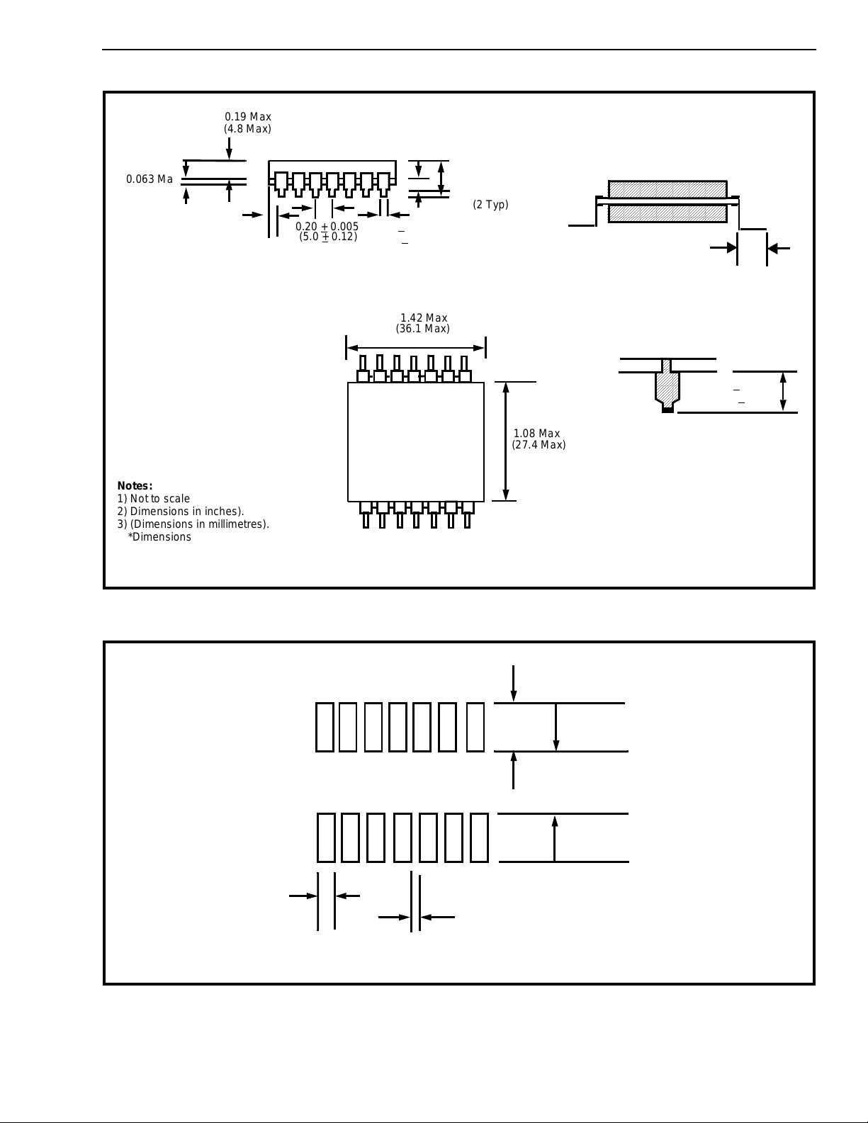
Figure 9 - Mechani cal Data for 14 Pin Surface M oun t Hybri d
0.1
(2.5)
0.89
(22.6)
0.04
(1.02)
0.16
(4.06)
Figure 10 - Recomme nde d Fo otpr int for 14 Pin Surface Mo un t Hybri d
2-31
Page 12

MH88422 Preliminary Information
Notes:
2-32
 Loading...