

Page 1
Preliminary Spec.
MITSUBISHI LSIs
MH32V7245BST -5, -6
HYPER PAGE MODE 2415919104 - BIT ( 33554432 - WORD BY 72 - BIT ) DYNAMIC RAM
DESCRIPTION
The MH32V7245BST is 33554432-word x 72-bit dynamic
ram stacked structural module. This consist of thirty-six
industry standard 16M x 4 dynamic RAMs in TSOP and
two industry standard input buffer in TSSOP.
The stacked structure of TSOP on a card edge dual in-line
package provides any application where high densities and
large of quantities memory are required.
This is a socket-type memory module ,suitable for easy
interchange or addition of module.
FEATURES
/RAS
/CAS Address /OE Cycle Power
access
access
access
Type name
MH32V7245BST-5
MH32V7245BST-6
Utilizes industry standard 16M x 4 RAMs TSOP and industry
standard input buffer in TSSOP
168-pin (84-pin dual dual in-line package) stacked structure
Single 3.3V(+/- 0.3V) supply operation
Low stand-by power dissipation . . . . . . . . . . 64.9mW(Max)
Low operation power dissipation
MH32V7245BST -5 . . . . . . . . . . . . . . . . . . 8.44W(Max)
MH32V7245BST -6 . . . . . . . . . . . . . . . . . . 7.79W(Max)
All input are directly LVTTL compatible
All output are three-state and directry LVTTL compatible
Includes(0.22 uF x 38) decoupling capacitors
4096 refresh cycle every 64ms (A0 - A11)
Hyper-page mpde,Read-modify-write,/CAS before /RAS refresh,
Hidden refresh capabilities
JEDEC standard pin configration & Buffered PD pin
Buffered input except /RAS and DQ
Gold plating contact pads
time
time
(max.ns)
(max.ns)
50 18 30 182084
60 20 35
time
(max.ns)
access
time
(max.ns)
time
(min.ns)
110
dissipation
(typ.W)
7.03
5.87
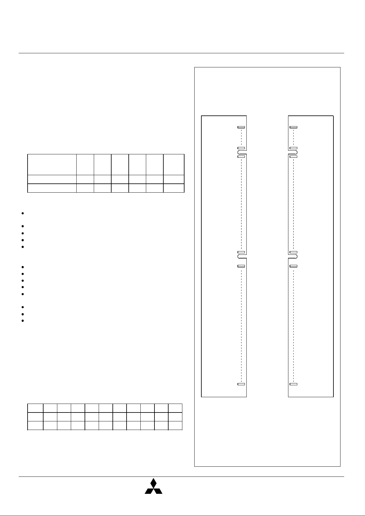
PIN CONFIGURATION
85pin
94pin
95pin
124pin
BACK SIDE
125pin
1pin
10pin
11pin
40pin
FRONT SIDE
41pin
APPLICATION
Main memory unit for computers , Microcomputer memory
PD&ID TABLE
PD1 PD2 PD3 PD4 PD5 PD6 PD7 PD8 ID0 ID1
- 5
1 0 0 0 1 0
- 6
1 0 0 0 1 1 1 0 0 0
- 7 1 0 0 0 1 0 1 0 0 0
1 = NC , 0 = drive to VOL
PD pin . . . buffered. When /PDE is low, PD information can be read
ID pin . . . non-buffered
1
MIT - DS - 0218-0.0
0
0 0
0
MITSUBISHI
ELECTRIC
168pin
84pin
13/JUL./1998
Page 2

Preliminary Spec.
MITSUBISHI LSIs
MH32V7245BST -5, -6
HYPER PAGE MODE 2415919104 - BIT ( 33554432 - WORD BY 72 - BIT ) DYNAMIC RAM
PIN CONFIGURATION
Pin No. Pin Name Pin No. Pin Name Pin No. Pin Name Pin No. Pin Name
1
2
3
4
5
6
7
8
9
10
11
12
13
14
15
16
17
18
19
20
21
22
23
24
25
26
27
28
29
30
31
32
33
34
35
36
37
38
39
40
41
42
Vss
DQ0
DQ1
DQ2
DQ3
Vcc
DQ4
DQ5
DQ6
DQ7
DQ8
Vss
DQ9
DQ10
DQ11
DQ12
DQ13
Vcc
DQ14
DQ15
DQ16
DQ17
Vss
Reserved
Reserved
Vcc
/WE0
/CAS0
Reserved
/RAS0
/OE0
Vss
A0
A2
A4
A6
A8
A10 A11
Reserved
Vcc
RFU
RFU
43
44
45
46
47
48
49
50
51
52
53
54
55
56
57
58
59
60
61
62
63
64
65
66
67
68
69
70
71
72
73
74
75
76
77
78
79
80
81
82
83
84
Vss
/OE2
/RAS2
/CAS4
Reserved
/WE2
Vcc
Reserved
Reserved
DQ18
DQ19
Vss
DQ20
DQ21
DQ22
DQ23
Vcc
DQ24
RFU
RFU
RFU
RFU
DQ25
DQ26
DQ27
Vss
DQ28
DQ29
DQ30
DQ31
Vcc
DQ32
DQ33
DQ34
DQ35
Vss
PD1
PD3
PD5
PD7
ID0
Vcc
85
86
87
88
89
90
91
92
93
94
95
96
97
98
99
100
101
102
103
104
105
106
107
108
109
110
111
112
113
114
115
116
117
118
119
120
121
122
123
124
125
126
Vss
DQ36
DQ37
DQ38
DQ39
Vcc
DQ40
DQ41
DQ42
DQ43
DQ44
Vss
DQ45
DQ46
DQ47
DQ48
DQ49
Vcc
DQ50
DQ51
DQ52
DQ53
Vss
Reserved
Reserved
Vcc
RFU
/CAS1
Reserved
/RAS1
RFU
Vss
A1
A3
A5
A7
A9
Reserved
Vcc
RFU
B0
127
128
129
130
131
132
133
134
135
136
137
138
139
140
141
142
143
144
145
146
147
148
149
150
151
152
153
154
155
156
157
158
159
160
161
162
163
164
165
166
167
168
RFU
/RAS3
/CAS5
Reserved
/PDE
Reserved
Reserved
DQ54
DQ55
DQ56
DQ57
DQ58
DQ59
DQ60
RFU
RFU
RFU
RFU
DQ61
DQ62
DQ63
DQ64
DQ65
DQ66
DQ67
DQ68
DQ69
DQ70
DQ71
PD2
PD4
PD6
PD8
Vss
Vcc
Vss
Vcc
Vss
Vcc
Vss
ID1
Vcc
Reserved: Reserved use
RFU: Reserved for future use
2
MIT - DS - 0218-0.0
MITSUBISHI
13/JUL./1998
ELECTRIC
Page 3
Preliminary Spec.
HYPER PAGE MODE 2415919104 - BIT ( 33554432 - WORD BY 72 - BIT ) DYNAMIC RAM
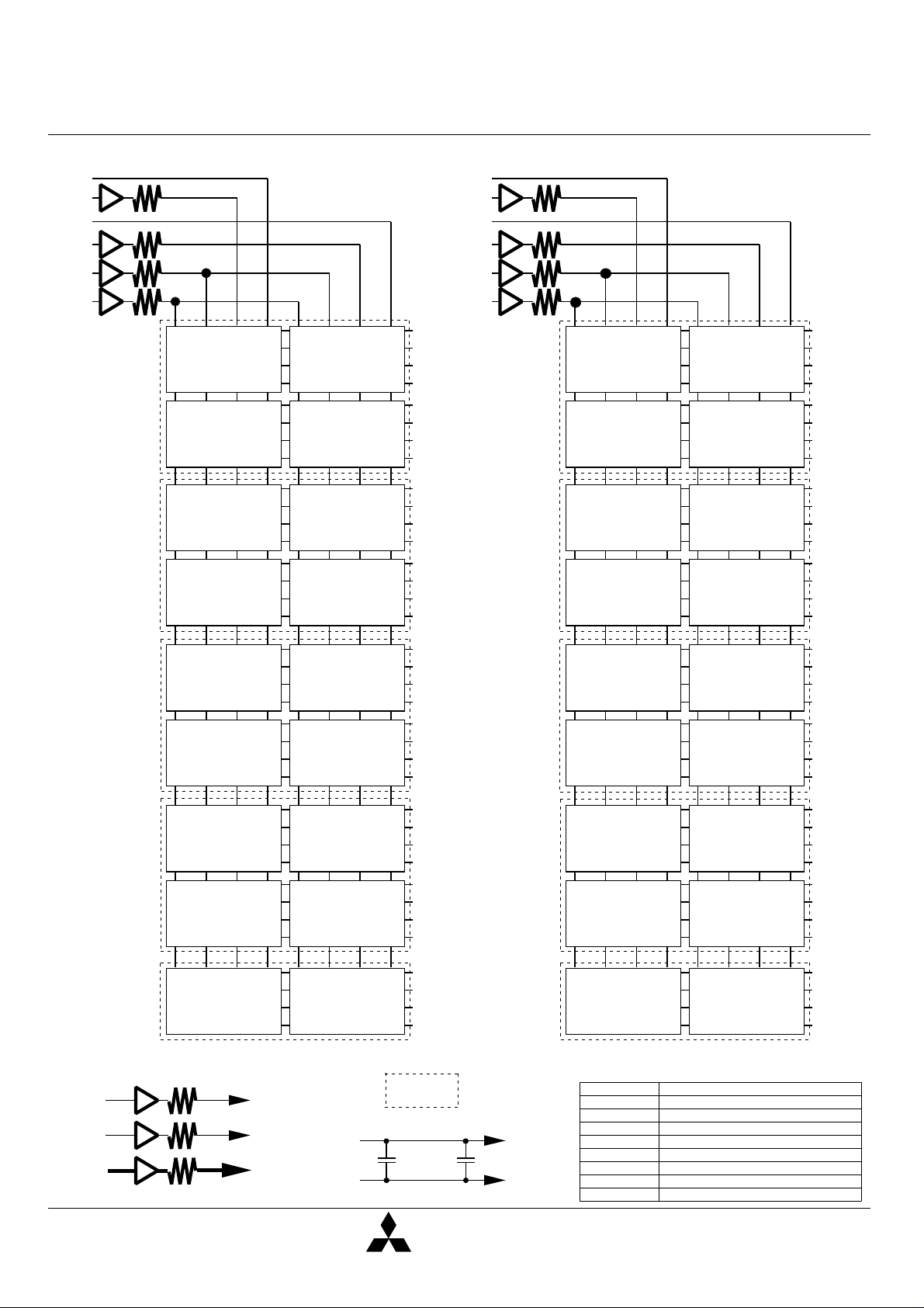
BLOCK DIAGRAM
MITSUBISHI LSIs
MH32V7245BST -5, -6
/RAS0
/CAS0
/RAS1
/CAS1
/WE0
/OE0
D0
D1
D2
D3
/RAS/CAS/W/OE
DQ1
~DQ4
/RAS/CAS/W/OE
DQ1
~DQ4
/RAS/CAS/W/OE
DQ1
~DQ4
/RAS/CAS/W/OE
DQ1
~DQ4
D18
D19
D20
D21
/RAS/CAS/W/OE
DQ1
~DQ4
/RAS/CAS/W/OE
DQ1
~DQ4
/RAS/CAS/W/OE
DQ1
~DQ4
/RAS/CAS/W/OE
DQ1
~DQ4
DQ0
DQ1
DQ2
DQ3
DQ4
DQ5
DQ6
DQ7
DQ8
DQ9
DQ10
DQ11
DQ12
DQ13
DQ14
DQ15
/RAS2
/CAS4
/RAS3
/CAS5
/WE2
/OE2
D9
D10
D11
D12
/RAS/CAS/W/OE
DQ1
~DQ4
/RAS/CAS/W/OE
DQ1
~DQ4
/RAS/CAS/W/OE
DQ1
~DQ4
/RAS/CAS/W/OE
DQ1
~DQ4
D27
D28
D29
D30
/RAS/CAS/W/OE
DQ1
~DQ4
/RAS/CAS/W/OE
DQ1
~DQ4
/RAS/CAS/W/OE
DQ1
~DQ4
/RAS/CAS/W/OE
DQ1
~DQ4
DQ36
DQ37
DQ38
DQ39
DQ40
DQ41
DQ42
DQ43
DQ44
DQ45
DQ46
DQ47
DQ48
DQ49
DQ50
DQ51
A0
B0
A1 - A11
/RAS/CAS/W/OE
DQ1
D4
~DQ4
/RAS/CAS/W/OE
DQ1
D5
~DQ4
/RAS/CAS/W/OE
DQ1
D6
~DQ4
/RAS/CAS/W/OE
DQ1
D7
~DQ4
/RAS/CAS/W/OE
DQ1
D8
~DQ4
D : M5M465405BTP
D0 - D8
D18 - D26
D9 - D17
D27 - D35
D0 - D35
D22
D23
D24
D25
D26
Vcc
Vss
/RAS/CAS/W/OE
DQ1
~DQ4
/RAS/CAS/W/OE
DQ1
~DQ4
/RAS/CAS/W/OE
DQ1
~DQ4
/RAS/CAS/W/OE
DQ1
~DQ4
/RAS/CAS/W/OE
DQ1
~DQ4
DQ16
DQ17
DQ18
DQ19
DQ20
DQ21
DQ22
DQ23
DQ24
DQ25
DQ26
DQ27
DQ28
DQ29
DQ30
DQ31
DQ32
DQ33
DQ34
DQ35
C1 - C20
. . .
Stacked Unit
D0 - D35
& INPUT BUFFER
/RAS/CAS/W/OE
DQ1
D13
~DQ4
/RAS/CAS/W/OE
DQ1
D14
~DQ4
/RAS/CAS/W/OE
DQ1
D15
~DQ4
/RAS/CAS/W/OE
DQ1
D16
~DQ4
/RAS/CAS/W/OE
DQ1
D17
~DQ4
PIN NAME FUNCTION
/RAS
/CAS
/WE
/OE
A, B
DQ
Vcc
Vss
ROW ADDRESS STROBE INPUT
COLUMN ADDRESS STROBE INPUT
WRITE CONTROL INPUT
OUTPUT ENABLE INPUT
ADDRESS INPUT
DATA I/O
POWER SUPPLY
GROUND
D31
D32
D33
D34
D35
DQ1
~DQ4
DQ1
~DQ4
DQ1
~DQ4
DQ1
~DQ4
DQ1
~DQ4
DQ52
/RAS/CAS/W/OE
DQ53
DQ54
DQ55
DQ56
/RAS/CAS/W/OE
DQ57
DQ58
DQ59
DQ60
/RAS/CAS/W/OE
DQ61
DQ62
DQ63
DQ64
/RAS/CAS/W/OE
DQ65
DQ66
DQ67
/RAS/CAS/W/OE
DQ68
DQ69
DQ70
DQ71
3
MIT - DS - 0218-0.0
MITSUBISHI
13/JUL./1998
ELECTRIC
Page 4
Preliminary Spec.
MH32V7245BST -5, -6
HYPER PAGE MODE 2415919104 - BIT ( 33554432 - WORD BY 72 - BIT ) DYNAMIC RAM
FUNCTION
The MH32V7245BST provide, in addition to normal read,
write, and read-modify-write operations,
Table 1 Input conditions for each mode
Operation
Read
Write (Early write)
Write (Delayed write)
Read-modify-write
Hidden refresh
/CAS before /RAS refresh
Standby
Note : ACT : active, NAC : nonactive, DNC : don' t care, VLD : valid, IVD : Invalid, APD : applied, OPN : open
/RAS /CAS
ACT
ACT
ACT
ACT
ACT
ACT
NAC
ACT
ACT
ACT
ACT
ACT
ACT
DNC
Inputs Input/Output
/W
NAC
ACT
ACT
ACT
DNC
NAC
DNC
a number of other functions, e.g., hyper page mode, /CAS
before /RAS refresh, and delayed-write. The input conditions
for each are shown in Table 1.
/OE
ACT
DNC
DNC
ACT
ACT
DNC
DNC
Row
address address
APD
APD
APD
APD
DNC
DNC
DNC
Column
APD
APD
APD
APD
DNC
DNC
DNC
Input
OPN
VLD
VLD
VLD
OPN
DNC
DNC
Output
VLD
OPN
IVD
VLD
VLD
OPN
OPN
MITSUBISHI LSIs
Refresh Remark
NO
NO
NO
NO
YES
YES
NO
Hyper page mode
identical
4
MIT - DS - 0218-0.0
MITSUBISHI
13/JUL./1998
ELECTRIC
Page 5
Preliminary Spec.
HYPER PAGE MODE 2415919104 - BIT ( 33554432 - WORD BY 72 - BIT ) DYNAMIC RAM
ABSOLUTE MAXIMUM RATINGS
Symbol
Vcc
IO
Pd
Topr
Tstg
Supply voltage
Output current
Power dissipation
Operating temperature
Storage temperature
MH32V7245BST -5, -6
Parameter Conditions
With respect to Vss
Ta=25°C
MITSUBISHI LSIs
Ratings
-0.5~4.6
50
20
0~70
-40~100
Unit
V
mA
W
°C
°C
RECOMMENDED OPERATING CONDITIONS
Symbol
Vcc
Vss
VIH
VIL
Note 1 : All voltage values are with respect to Vss
Supply voltage
Supply voltage
High-level input voltage, all inputs
Low-level input voltage
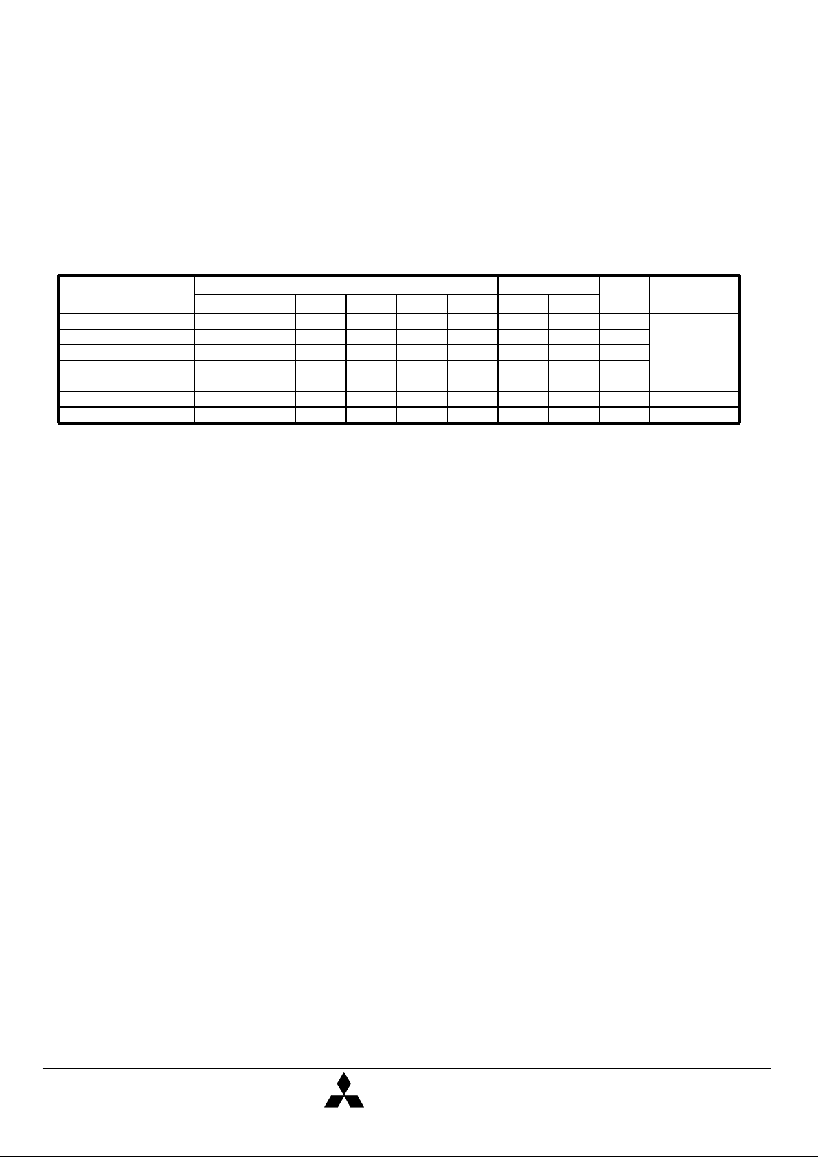
ELECTRICAL CHARACTERISTICS
Symbol
VOH
VOL
IOZ
I I
I I (RAS)
ICC1 (AV)
ICC2
ICC4(AV)
ICC6(AV)
Note 2: Current flowing into an IC is positive, out is negative.
3: Icc1 (AV), Icc3 (AV), Icc4 (AV) and Icc6 (AV) are dependent on cycle rate. Maximum current is measured at the fastest cycle rate.
4: Icc1 (AV) and Icc4 (AV) are dependent on output loading. Specified values are obtained with the output open.
5: Under condition of colmun address being changed once or less while /RAS=VIL and /CAS=VIH
High-level output voltage
Low-level output voltage
Off-state output current
Input current (except /RAS)
Input current (/RAS)
Average supply
current
from Vcc operating
Supply current from Vcc , stand-by
Average supply current
from Vcc
Hyper-Page-Mode
Average supply current from Vcc
/CAS before /RAS refresh
mode
Parameter
Parameter
(Ta=0~70°C, Vcc=3.3V ± 0.3V, Vss=0V, unless otherwise noted) (Note 2)
- 5
(Note 3,4,5)
- 6
- 5
(Note 3,4,5)
- 6
- 5
(Note 3,5)
- 6
(Ta=0~70°C, unless otherwise noted) (Note 1)
Limits
Min Nom Max
3.6
3.3
3.0
0
0
2.0
-0.3
IOH=-2.0mA
IOL=2.0mA
Q floating 0V VOUT Vcc
VII
0V VIN Vcc+0.3V, Other input pins=0V
VII
0V VIN Vcc+0.3V, Other input pins=0V
/RAS, /CAS cycling
tRC=tWC=min.
output open
/RAS=/CAS =VIH, output open
/RAS=/CAS Vcc -0.2, output open
/RAS=VIL,/CAS cycling
tPC=min.
output open
/CAS before /RAS refresh cycling
tRC=min.
output open
Vcc+0.3
0.8
Test conditions
VII
VII
VII
IIV
Unit
V
0
V
V
V
VII
Min
2.4
0
-20
-10
-90
Limits
Typ
Max
Vcc
0.4
20
10
90
2378
2198
56
38
1838
1658
2378
2198
Unit
V
V
µA
µA
µA
mA
mA
mA
mA
CAPACITANCE
Symbol Parameter
5
CI (/RAS)
C(DQ)
MIT - DS - 0218-0.0
Input capacitance, /RAS input
Input capacitance, except /RAS input 15
Input/Output capacitance,DATA
(Ta = 0~70°C, Vcc = 3.3V ± 0.3V, Vss = 0V, unless otherwise noted)
Test conditions
VI=Vss
f=1MHZ
Vi=25mVrms
MITSUBISHI
ELECTRIC
Limits
Min Max
Typ
80
25
13/JUL./1998
Unit
pF
pFCI
pF
Page 6
Preliminary Spec.
MITSUBISHI LSIs
MH32V7245BST -5, -6
HYPER PAGE MODE 2415919104 - BIT ( 33554432 - WORD BY 72 - BIT ) DYNAMIC RAM
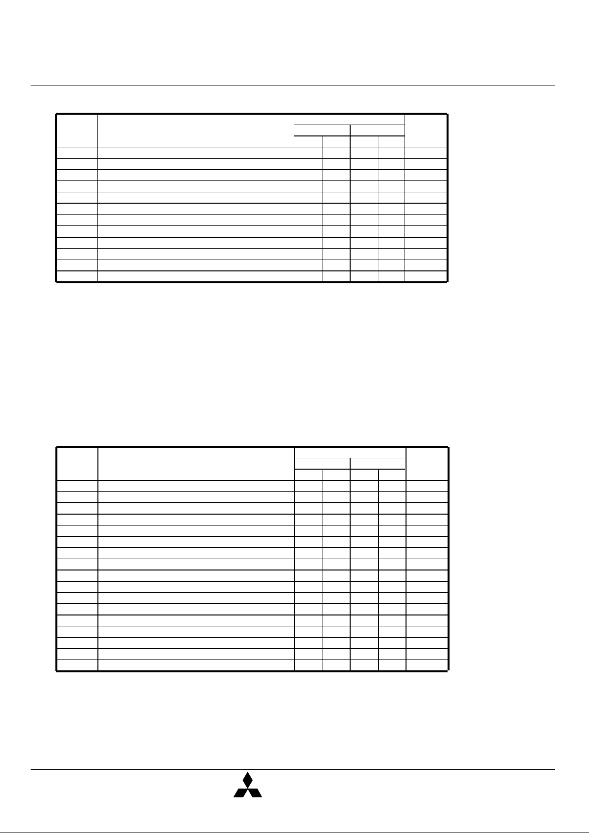
SWITCHING CHARACTERISTICS
(Ta=0~70°C, Vcc=3.3V ± 0.3V, Vss=0V, unless otherwise noted , see notes 6,14,15)
Limits
ParameterSymbol Unit
- 5
Min Max
tCAC
tRAC
tAA
tCPA
tOEA
tOHC Output hold time from /CAS
tOHR
tCLZ
tOEZ
tWEZ Output disable time after /WE high (Note 12)
tOFF
tREZ
Note 6: An initial pause of 500 us is required after power-up followed by a minimum of eight initialization cycles (any combination of cycles containing a /CAS before /RAS refresh).
Note the /RAS may be cycled during the initial pause . And any 8 /RAS or /RAS /CAS cycles are required after prolonged periods (greater than 64 ms) of /RAS inactivity
before proper device operation is achieved.
7: Measured with a load circuit equivalent to 1TTL loads and 50pF,VOH=2.4V(IOH=-2mA) and VOL=0.4V(IOL=-2mA).
The reference levels for measuring of output signals are 2.0V(VOH) and 0.8V(VOL).
8: Assumes that tRCD tRCD(max), tASC tASC(max) and tCP tCP(max).
9: Assumes that tRCD tRCD(max) and tRAD tRAD(max). If tRCD or tRAD is greater than the maximum recommended value shown in this table, tRAC will
increase by amount that tRCD exceeds the value shown.
10: Assumes that tRAD tRAD(max) and tASC tASC(max).
11: Assumes that tCP tCP(max) and tASC tASC(max).
12: tOEZ (max), tWEZ(max), tOFF(max) and tREZ(max) defines the time at which the output achieves the high impedance state (IOUT I +/- 10 uAI) and is not
reference to VOH(min) or VOL(max).
13: Output is disable after both /RAS and /CAS go to high.
Access time from /CAS
Access time from /RAS
Columu address access time
Access time from /CAS precharge
Access time from /OE
Output hold time from /RAS
Output low impedance time from /CAS low
(Note 7,8)
(Note 7,9)
(Note 7,10)
(Note 7,11)
(Note 7)
(Note 13)
(Note 7)
Output disable time after /OE high (Note 12)
Output disable time after /CAS high
Output disable time after /RAS high
IIV
VII
IIV
VII
IIV
VII
VII
IIV
(Note 12,13)
(Note 12,13)
IIV
18
50
30
33
18
10
5
10
18
18
18
13
- 6
Min Max
20
60
35
38
20
10
5
10
20
20
20
15
ns
ns
ns
ns
ns
ns
ns
ns
ns
ns
ns
ns
VII
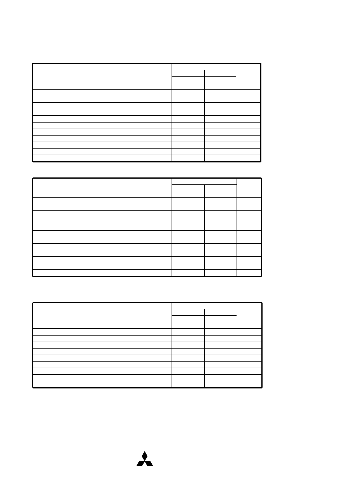
TIMING REQUIREMENTS (For Read, Write, Read-Modify-Write ,Refresh, and Hyper-Page Mode Cycles)
(Ta=0~70°C, Vcc=3.3V ± 0.3V, Vss=0V, unless otherwise noted ,see notes 14,15)
Limits
ParameterSymbol
-5
Min Max
tREF
tRP
tRCD
tCRP
tRPC
tCPN
tRAD
tASR
tASC
tRAH
tCAH
tDZC
tDZO
tRDD
tCDD
tODD
tT Transition time
Note 14: The timing requirements are assumed tT =2ns.
15: VIH(min) and VIL(max) are reference levels for measuring timing of input signals.
16: tRCD(max) is specified as a reference point only. If tRCD is less than tRCD(max), access time is tRAC. If tRCD is greater than tRCD(max), access time is
controlled exclusively by tCAC or tAA. .
17: tRAD(max) is specified as a reference point only. If tRAD tRAD(max) and tASC tASC(max), access time is controlled exclusively by tAA.
18: tASC(max) is specified as a reference point only. If tRCD tRCD(max) and tASC tASC(max), access time is controlled exclusively by tCAC.
19: Either tDZC or tDZO must be satisfied.
20: Either tRDD or tCDD or tODD must be satisfied.
21: tT is measured between VIH(min) and VIL(max).
Refresh cycle time
/RAS high pulse width
Delay time, /RAS low to /CAS low
Delay time, /CAS high to /RAS low
Delay time, /RAS high to /CAS low
/CAS high pulse width
Column address delay time from /RAS low
Row address setup time before /RAS low
Column address setup time before /CAS low
Row address hold time after /RAS low
Column address hold time after /CAS low
Delay time, data to /CAS low
Delay time, data to /OE low
Delay time, /RAS high to data
Delay time, /CAS high to data
Delay time, /OE high to data
IIV
IIV
(Note16)
(Note17)
(Note18)
(Note19)
(Note19)
(Note20)
(Note20)
(Note20)
(Note21)
64
30
32
9
10
0
8
5
20
5
0
10 13
3
8
0
0
13
18
18
501
VII
IIV
-6
Min Max
64
40
40
9
10
0
10
7
25
5
0
5
10
0
0
15
20
20
50
1 ns
Unit
ms
ns
ns
ns
ns
ns
ns
ns
ns
ns
ns
ns
ns
ns
ns
ns
6
MIT - DS - 0218-0.0
MITSUBISHI
13/JUL./1998
ELECTRIC
Page 7
Preliminary Spec.
MH32V7245BST -5, -6
HYPER PAGE MODE 2415919104 - BIT ( 33554432 - WORD BY 72 - BIT ) DYNAMIC RAM
Read and Refresh Cycles
Limits
ParameterSymbol Unit-6
tRC
tRAS
tCAS
tCSH
tRSH
tRCS
tRCH
tRRH
tRAL
tCAL
tORH
tOCH /CAS hold time after /OE iow ns
Note 22: Either tRCH or tRRH must be satisfied for a read cycle.
Read cycle time
/RAS iow pulse width
/CAS iow pulse width
/CAS hold time after /RAS iow
/RAS hold time after /CAS iow
Read Setup time after /CAS high
Read hold time after /CAS iow
Read hold time after /RAS iow
Column address to /RAS hold time
Column address to /CAS hold time
/RAS hold time after /OE iow
(Note 22)
(Note 22)
Write Cycle (Early Write and Delayed Write)
ParameterSymbol Unit
tWC
tRAS
tCAS
tCSH
tRSH
tWCS
tWCH
tCWL
tRWL
tWP
tDS
tDH
Write cycle time
/RAS iow pulse width
/CAS iow pulse width
/CAS hold time after /RAS iow
/RAS hold time after /CAS low
Write setup time before /CAS low
Write hold time after /CAS low
/CAS hold time after /W low
/RAS hold time after W low
Write pulse width
Data setup time before /CAS low or W low
Data hold time after /CAS low or W low
(Note 24)
-5
Min Max
84
50
10000
8
10000
30
18
0
0
0
30
13
18
13
-5
Min Max
84
10000
50
10000
8
30
18
0
8
8
13
8
-5
13
Min Max
104
60
10
43
20
0
35
18
20
15
Limits
Min Max
104
60
10
35
20
10
10
15
10
-5
15
MITSUBISHI LSIs
ns
10000
10000
0
0
-6
10000
10000
0
ns
ns
ns
ns
ns
ns
ns
ns
ns
ns
ns
ns
ns
ns
ns
ns
ns
ns
ns
ns
ns
ns
Read-Write and Read-Modify-Write Cycles
Limits
ParameterSymbol
tRWC
tRAS
tCAS
tCSH
tRSH
tRCS
tCWD
tRWD
tAWD
tOEH
Note 23: tRWC is specified as tRWC(min)=tRAC(max)+tODD(min)+tRWL(min)+tRP(min)+4tT.
24:tWCS, tCWD,tRWD ,tAWD and,tCPWD are specified as reference points only. If tWCS tWCS(min) the cycle is an early write cycle and the DQ pins will remain
high impedance throughout the entire cycle. If tCWD tCWD(min), tRWD tRWD (min), tAWD tAWD(min) and tCPWD tCPWD(min) (for Fast page mode cycle
only), the cycle is a read-modify-write cycle and the DQ will contain the data read from the selected address. If neither of the above condition (delayed write) of the
DQ (at access time and until /CAS or /OE goes back to VIH) is indeteminate.
7
MIT - DS - 0218-0.0
Read write/read modify write cycle time
/RAS low pulse width
/CAS low pulse width
/CAS hold time after /RAS low
/RAS hold time after /CAS low
Read setup time before /CAS low
Delay time, /CAS low to /W low
Delay time, /RAS low to /W low
Delay time, address to /W low
OE hold time after W low
IIV
(Note23)
(Note24)
(Note24)
(Note24)
IIV
MITSUBISHI
-5
Min Max
109
75
10000
38
10000
65
43
0
28
60
40
13
IIV
IIV
-6
Min Max
133
89
10000
44
10000
77
49
0
32
72
47
15
Unit
ns
ns
ns
ns
ns
ns
ns
ns
ns
ns
IIV
13/JUL./1998
ELECTRIC
Page 8

Preliminary Spec.
MH32V7245BST -5, -6
HYPER PAGE MODE 2415919104 - BIT ( 33554432 - WORD BY 72 - BIT ) DYNAMIC RAM
Hyper Page Mode Cycle (Read, Early Write, Read -Write, Read-Modify-Write Cycle,
Read Write Mix Cycle,Hi-Z control by /OE or /W) (Note 25)
Limits
ParameterSymbol
tHPC
tHPRWC
tDOH
tRAS
tCP
tCPRH
tCPWD
tCHOL
tOEPE
tWPE
tHCWD
tHAWD
tHPWD
tHCOD
tHAOD
tHPOD
Note 25: All previously specified timing requirements and switching characteristics are applicable to their respective Hyper page mode cycle.
26: tRAS(min) is specified as two cycles of /CAS input are performed.
27: tCP(max) is specified as a reference point only.
Hyper page mode read/write cycle time
Hyper page mode read write/read modify write cycle time
Output hold time from /CAS low
/RAS low pulse width for read write cycle
/CAS high pulse width
/RAS hold time after /CAS precharge
Delay time,/CAS precharge to /W low
Hold time to maintain the data Hi-Z until /CAS access
/OE Pulse width(Hi-Z control)
/W Pulse width(Hi-Z control)
Delay time,/CAS low to /W low after read
Delay time, Address to /W low after read
Delay time,/CAS precharge to /W low after read
Delay time,/CAS low to /OE high after read
Delay time,Address to /OE high after read
Delay time, /CAS precharge to /OE high after read
(Note26)
(Note27)
(Note24)
-5
Min Max
20
55
10
100000
65
8
33
43
7
7
7
28
40
43
13
25
28
15 16
-6
Min Max
25
66
10
100000
77
10
38
50
7
7
7
32
47
50
15
30
33
Unit
ns
ns
ns
ns
ns
ns
ns
ns
ns
ns
ns
ns
ns
ns
ns
ns
MITSUBISHI LSIs
/CAS before /RAS Refresh Cycle (Note 28)
Limits
ParameterSymbol Unit
tCSR
tCHR
tRSR
tRHR
Note 28: Eight or more /CAS before /RAS cycles instead of eight /RAS cycles are necessary for proper operation of /CAS before /RAS refresh
mode.
/CAS setup time before /RAS low
/CAS hold time after /RAS low
Read setup time before /RAS low
Read hold time after /RAS low
-5
Min Max
10
5
15
5
-6
Min Max
10
5
15
5
ns
ns
ns
ns
8
MIT - DS - 0218-0.0
MITSUBISHI
13/JUL./1998
ELECTRIC
Page 9

Preliminary Spec.
Timing Diagrams (Note 29)
Read Cycle
MITSUBISHI LSIs
MH32V7245BST -5, -6
HYPER PAGE MODE 2415919104 - BIT ( 33554432 - WORD BY 72 - BIT ) DYNAMIC RAM
tRC
/RAS
/ CAS
A0,B0~A11
/W
DQ
(INPUTS)
DQ
(OUTPUTS)
/OE
VIH
VIL
VIH
VIL
VIH
VIL
VIH
VIL
VIH
VIL
VOH
VOL
VIH
VIL
tCRP
tASR tRAH
ROW
ADDRESS
tRAD
tRCD
tDZC
tASC tCAH
tRCS
tRAC
COLUMN
ADDRESS
tCLZ
tDZO
tRAS
tCAC
tAA
tCSH
tOEA
tRAL
tCAL
tCAS
Hi-Z
tRSH
tOCH
tRDD
tREZ
tOHR
DATA VALID
tRP
tCRP
tASR
ROW
ADDRESS
tRRH
tRCH
tCDD
tWEZ
tOFF
tOHC
Hi-ZHi-Z
tOEZ
tODD
tORH
Note 29
Indicates the don't care input.
VIH(min) VIN VIH(max) or VIL(min) VIN VIL(max)
VII
VII
VII
VII
Indicates the invalid output.
9
MIT - DS - 0218-0.0
MITSUBISHI
13/JUL./1998
ELECTRIC
Page 10

Preliminary Spec.
Early Write Cycle
MITSUBISHI LSIs
MH32V7245BST -5, -6
HYPER PAGE MODE 2415919104 - BIT ( 33554432 - WORD BY 72 - BIT ) DYNAMIC RAM
tWC
/RAS
/CAS
A0,B0~A11
/W
DQ
(INPUTS)
VIH
VIL
VIH
VIL
VIH
VIL
VIH
VIL
VIH
VIL
tCRP
tASR
tRAH
ROW COLUMN
ADDRESS
tRCD
tASC
tWCS
tDS
tRAS
tCAH
ADDRESS
DATA VALID
tWCH
tDH
tCSH
tRSH
tCAS
tRP
tCRP
tASR
ROW
ADDRESS
10
DQ
(OUTPUTS)
/OE
VOH
VOL
VIH
VIL
MIT - DS - 0218-0.0
Hi-Z
MITSUBISHI
ELECTRIC
13/JUL./1998
Page 11

Preliminary Spec.
Delayed Write Cycle
MITSUBISHI LSIs
MH32V7245BST -5, -6
HYPER PAGE MODE 2415919104 - BIT ( 33554432 - WORD BY 72 - BIT ) DYNAMIC RAM
tWC
/RAS
/ CAS
A0,B0~A11
/W
DQ
(INPUTS)
VIH
VIL
VIH
VIL
VIH
VIL
VIH
VIL
VIH
VIL
tCRP
tASR tRAH
ROW
ADDRESS
tRCD
tASC
tRCS
tDZC
tCSH
tCLZ
tRAS
tCAH
COLUMN
ADDRESS
Hi-Z
tRSH
tCAS
tWCH
tDS
tRP
tCRP
tASR
ROW
ADDRESS
tCWL
tRWL
tWP
tDH
DATA
VALID
11
DQ
(OUTPUTS)
/OE
MIT - DS - 0218-0.0
VOH
VOL
VIH
VIL
Hi-Z
tDZO
MITSUBISHI
ELECTRIC
tOEZ
Hi-Z
tOEH
tODD
13/JUL./1998
Page 12

Preliminary Spec.
HYPER PAGE MODE 2415919104 - BIT ( 33554432 - WORD BY 72 - BIT ) DYNAMIC RAM
Read-Write, Read-Modify-Write Cycle
MITSUBISHI LSIs
MH32V7245BST -5, -6
tRWC
/RAS
/ CAS
A0,B0~A11
/W
DQ
(INPUTS)
DQ
(OUTPUTS)
/OE
VIH
VIL
VIH
VIL
VIH
VIL
VIH
VIL
VIH
VIL
VOH
VOL
VIH
VIL
tCRP
tASR
tRAS
tCSH
tRCD
tRAD
tRAH
ROW
ADDRESS ADDRESS
Hi-Z
tASC
tRCS
tDZC
tRAC
tDZO
tCAH
COLUMN
Hi-Z
tCAC
tAA
tCLZ
tOEA
tAWD
tCWD
tRWD
DATA
VALID
tRSH
tCAS
tOEZ
tDS
tODD
tRP
tCRP
tASR
ROW
ADDRESS
tCWL
tRWL
tWP
tDH
DATA VALID
Hi-Z
tOEH
12
MIT - DS - 0218-0.0
MITSUBISHI
ELECTRIC
13/JUL./1998
Page 13

Preliminary Spec.
HYPER PAGE MODE 2415919104 - BIT ( 33554432 - WORD BY 72 - BIT ) DYNAMIC RAM
Hyper Page Mode Read Cycle
MITSUBISHI LSIs
MH32V7245BST -5, -6
/RAS
/ CAS
A0,B0~A11
/W
DQ
(INPUTS)
DQ
(OUTPUTS)
/OE
VIH
VIL
VIH
VIL
VIH
VIL
VIH
VIL
VIH
VIL
VOH
VOL
VIL
VIH
tCRP
tASR
ADDRESS
ROW
tRAH
Hi-Z
tRAD
tCSH tHPC
tRCD
tASC
COLUMN-1
tRCS
tDZC
tRAC
tDZO tOEA
tCAS
tCAH
tCAL tCAL tCAL
tCAC
tAA
tCLZ
VALID-1
tOCH
tRAS
tCP
DATA
tCAS
tCAHtASC tCAHtASC
COLUMN-2 COLUMN-3
Hi-Z
tCAC
tAA
tDOH
DATA
VALID-2
tCPA
tRSH
tCP tCAS
tCPRH
tCAC
tAA
tDOH
tCPA
tRP
tASR
ROW
ADDRESS
tRRH
tRCH
tWEZ
tRDD
tCDD
tREZ
tOHR
tOFF
tOHC
DATA
VALID-3
tOEZ
tODD
13
MIT - DS - 0218-0.0
MITSUBISHI
ELECTRIC
13/JUL./1998
Page 14

Preliminary Spec.
HYPER PAGE MODE 2415919104 - BIT ( 33554432 - WORD BY 72 - BIT ) DYNAMIC RAM
Hyper Page Mode Early Write Cycle
MITSUBISHI LSIs
MH32V7245BST -5, -6
/RAS
/ CAS
A0,B0~A11
/W
DQ
(INPUTS)
VIH
VIL
VIH
VIL
VIH
VIL
VIH
VIL
VIH
VIL
tCRP
tASR
tRAH
ROW
ADDRESS
tRAS
tCSH
tRCD
tASC
COLUMN-1
tWCS
tDS tDH tDS tDH tDS tDH
VALID-1
tCAS
tCAH
tWCH tWCS tWCH tWCS tWCH
DATA
tHPC
tCP
tASC
VALID-2
tCAS
tCAL tCAL
tCAH
COLUMN-2 COLUMN-3
DATA
tRSH
tCP tCAS
tASC
tCAH
DATA
VALID-3
tRP
tCRP
tASR
ROW
ADDRESS
14
DQ
(OUTPUTS)
/OE
MIT - DS - 0218-0.0
VOH
VOL
VIL
VIH
Hi-Z
MITSUBISHI
ELECTRIC
13/JUL./1998
Page 15

Preliminary Spec.
HYPER PAGE MODE 2415919104 - BIT ( 33554432 - WORD BY 72 - BIT ) DYNAMIC RAM
Hyper Page Mode Read-Write,Read-Modify-Write Cycle
MITSUBISHI LSIs
MH32V7245BST -5, -6
/RAS
/ CAS
A0,B0~A11
/W
DQ
(INPUTS)
DQ
(OUTPUTS)
/OE
VIH
VIL
VIH
VIL
VIH
VIL
VIH
VIL
VIH
VIL
VOH
VOL
VIH
VIL
tCRP
tASR
ADDRESS
ROW
tRAH
Hi-Z
tRCD
tRAD
tASC
tRCS
tDZC
tCLZ
tRAC
tDZO
tRAS
tCSH
tCAS
tCP
tCAH
COLUMN-1
tAWD
tCWD
tRWD
Hi-Z Hi-Z
tCAC
tAA
DATA
VALID-1
tOEA
tCWL
tDS
DATA
VALID-1
Hi-Z Hi-Z
tODD
tOEZ
tWP
tDH
tASC
COLUMN-2
tRCS
tDZC
tCPA
tDZO
tAA
tCAH
tAWD
tCPWD
tCAC
tOEA
tHPRWC
tCAS
tCWD
tCLZ
DATA
VALID-2
tDS
tODD
tOEZ
tRWL
tCWL
tWP
DATA
VALID-2
tOEH
tRP
tCRP
tASR
ROW
ADDRESS
tDH
15
MIT - DS - 0218-0.0
MITSUBISHI
ELECTRIC
13/JUL./1998
Page 16

Preliminary Spec.
Hyper Page Mode Mix Cycle (1)
MITSUBISHI LSIs
MH32V7245BST -5, -6
HYPER PAGE MODE 2415919104 - BIT ( 33554432 - WORD BY 72 - BIT ) DYNAMIC RAM
/RAS
/ CAS
A0,B0~A11
DQ
(INPUTS)
/W
VIH
VIL
VIH
VIL
VIH
VIL
VIH
VIL
VIH
VIL
tCRP
tASR
ADDRESS
ROW
tRAH
tRAD
tRCD
tASC
tCSH
COLUMN-1
tRCS
tDZC
tAA
tCAH
tCAL
tCAC
tCLZ
tCAS
tCP
tWCS
tDS
tRAS
tHPC
tCAS tCP
tCAHtASC tCAHtASC
COLUMN-2
tWCH
tCAL
tDH
DATA
VALID-2
tWEZ
tDZ
C
COLUMN-3
tCPWD
tAA
tCAC
tCLZ
tAWD
tCWD
tHPRWC
tCAS
tDS
tDH
DATA
VALID-3
tRWL
tCWL
tWP
tRP
tCRP
tASR
ADDRESS
ROW
DQ
(OUTPUTS)
16
VOH
VOL
VIL
/OE
VIH
MIT - DS - 0218-0.0
Hi-Z
tRAC
tDZO tOEA
DATA
VALID-1
tOEZ
tOCH
tODD
MITSUBISHI
ELECTRIC
tDZO
tCPA
tOEA
DATA
VALID-3
tOEZ
tODD
tOEH
13/JUL./1998
Page 17

Preliminary Spec.
HYPER PAGE MODE 2415919104 - BIT ( 33554432 - WORD BY 72 - BIT ) DYNAMIC RAM
Hyper Page Mode Mix Cycle (2)
MITSUBISHI LSIs
MH32V7245BST -5, -6
/RAS
/ CAS
A0,B0~A11
/W
DQ
(INPUTS)
DQ
(OUTPUTS)
/OE
VIH
VIL
VIH
VIL
VIH
VIL
VIH
VIL
VIH
VIL
VOH
VOL
VIL
VIH
tHPC
tCP tCAS
tASC
tCAH
COLUMN-1
tCAL
tHCWD
tHAWD
tHPWD
Hi-Z
tCAC
tAA
tCPA
tHCOD
tHAOD
tHPOD
tRCH
DATA
VALID-1
tWEZ
tOEZ
tCAS
tASC
tWCS
tDS
tODD
tCAH
COLUMN-2 COLUMN-3
tCAL
tWCH
tDH
DATA
VALID-2
Hi-Z
tDZC
tASC
tDZC
tCLZ
tCAC
tAA
tCPA
tOEA
tCAH
Hi-Z
DATA
VALID-3
17
MIT - DS - 0218-0.0
MITSUBISHI
ELECTRIC
13/JUL./1998
Page 18

Preliminary Spec.
HYPER PAGE MODE 2415919104 - BIT ( 33554432 - WORD BY 72 - BIT ) DYNAMIC RAM
Hyper Page Mode Read Cycle ( Hi-Z control by OE )
MITSUBISHI LSIs
MH32V7245BST -5, -6
/RAS
/ CAS
A0,B0~A11
/W
DQ
(INPUTS)
DQ
(OUTPUTS)
/OE
VIH
VIL
VIH
VIL
VIH
VIL
VIH
VIL
VIH
VIL
VOH
VOL
VIL
VIH
tCRP
tASR
tRAH
ROW
ADDRESS
tRAD
Hi-Z
tRCD
tASC
tRCS
tDZC
tRAC
tDZO
tCSH
tCAH
COLUMN-1
tCAC
tAA
tCLZ
tOEA
tCAS
DATA
VALID-1
tOEZ
tRAS
tHPC
tCP
VALID-1
tOCH
tOEA
tOEPE
tCAS
tCAHtASC
COLUMN-2 COLUMN-3
Hi-Z
tCAC
tAA
tDOH
DATA
tCPA
DATA
VALID-2
tCHOL
tCP
tASC
Hi-Z
tCPA
tOEZ
tOEPE
tCPRH
tCAH
tRAL
tCAC
tAA
tCLZ
tRSH
tCAS
tRP
tCRP
tASR
ROW
ADDRESS
tRRH
tRCH
tWEZ
tRDD
tCDD
tREZ
tOHR
tOFF
tOHC
DATA
VALID-3
tOEZ
tODD
18
MIT - DS - 0218-0.0
MITSUBISHI
ELECTRIC
13/JUL./1998
Page 19

Preliminary Spec.
HYPER PAGE MODE 2415919104 - BIT ( 33554432 - WORD BY 72 - BIT ) DYNAMIC RAM
Hyper Page Mode Read Cycle ( Hi-Z control by W )
MITSUBISHI LSIs
MH32V7245BST -5, -6
/RAS
/ CAS
A0,B0~A11
DQ
(INPUTS)
DQ
(OUTPUTS)
/OE
/W
VIH
VIL
VIH
VIL
VIH
VIL
VIH
VIL
VIH
VIL
VOH
VOL
VIL
VIH
tCRP
tASR
tRAH
ROW
ADDRESS
Hi-Z
tRAD
tCSH
tRCD
tASC
tRCS
tDZC
tRAC
tDZO tOEA
tCAH
COLUMN-1
tCAC
tAA
tCLZ
tCAS
tOCH
tRAS
tHPC
tCP
tASC tCAHtASC
DATA
VALID-1
tCAS
tCAH
COLUMN-2 COLUMN-3
tRCH
Hi-Z
tCAC
tAA
tDOH
DATA
VALID-2
tCPA
tRSH
tCP tCAS
tCPRH
tRAL
tRCS
tWPE
tCAC
tAA
tWEZ
tCLZ
Hi-Z
tCPA
tRP
tCRP
tASR
ROW
ADDRESS
tRRH
tRCH
tRDD
tCDD
tREZ
tOHR
tOFF
tOHC
DATA
VALID-3
tOEZ
tODD
19
MIT - DS - 0218-0.0
MITSUBISHI
ELECTRIC
13/JUL./1998
Page 20

Preliminary Spec.
HYPER PAGE MODE 2415919104 - BIT ( 33554432 - WORD BY 72 - BIT ) DYNAMIC RAM
/CAS before /RAS Refresh Cycle
MITSUBISHI LSIs
MH32V7245BST -5, -6
/RAS
/ CAS
A0,B0~A11
/W
DQ
(INPUTS)
DQ
(OUTPUTS)
VIH
VIL
VIH
VIL
VIH
VIL
VIH
VIL
VIH
VIL
VOH
VOL
tRPC
tRRH
tRCH
tRP
tCPN
tREZ
tOHR
tOFF
tOHC
tCSR
tCHR
tRAS
tRC
tRPC
tCSR
tCHR
Hi-Z
tRAS
tRC
tRPC
tRP
tCRP
tASR
ROW
ADDRESS
COLUMN
ADDRESS
tRCS
20
/OE
VIH
VIL
MIT - DS - 0218-0.0
tOEZ
MITSUBISHI
ELECTRIC
13/JUL./1998
Page 21

Preliminary Spec.
HYPER PAGE MODE 2415919104 - BIT ( 33554432 - WORD BY 72 - BIT ) DYNAMIC RAM
Hidden Refresh Cycle (Read) (Note 31)
MITSUBISHI LSIs
MH32V7245BST -5, -6
/RAS
/ CAS
A0,B0~A11
/W
DQ
(INPUTS)
DQ
(OUTPUTS)
/OE
VIH
VIL
VIH
VIL
VIH
VIL
VIH
VIL
VIH
VIL
VOH
VOL
VIH
VIL
tCRP
tASR
tRAH
ROW
ADDRESS
tRCD
tRAD
tASC
tRCS
tDZC
Hi-Z
tRAC
tDZO tOEA
tRC
tRAS
tCAH
COLUMN
ADDRESS
tRAL
tCAC
tAA
tCLZ
tRSH
tORH
tRP
tCHR
Hi-Z
DATA VALID
tRAS
tRC
tRP
tASR
ROW
ADDRESS
tRRH
tRCH
tCDD
tRDD
tREZ
tOHR
tOFF
tOHC
Hi-Z
tOEZ
tODD
21
Note 31: Early write, delayed write, read write or read modify write cycle is applicable instead of read cycle.
Timing requirements and output state are the same as that of each cycle shown above.
MIT - DS - 0218-0.0
MITSUBISHI
ELECTRIC
13/JUL./1998
Page 22

Preliminary Spec.
133.35±0.13
127.35±0.133±0.13
1±0.13
R2±0.13
Package outline
38.1±0.13
17.78±0.13
3±0.13
MITSUBISHI LSIs
MH32V7245BST -5, -6
HYPER PAGE MODE 2415919104 - BIT ( 33554432 - WORD BY 72 - BIT ) DYNAMIC RAM
6.77Max
5.1Min
1.27±0.1
5.1Min
23.495±0.13 43.18±0.13
MIT - DS - 0218-0.0
MITSUBISHI
ELECTRIC
13/JUL./1998
 Loading...