

Page 1
Preliminary Spec.
DESCRIPTION
Type name
133MHz
5.4nsMH32S72DBFA-6
TSOP package , industry standard Resister in TSSOP package ,
Frequency
(CL = 4)
Some contents are subject to change without notice.
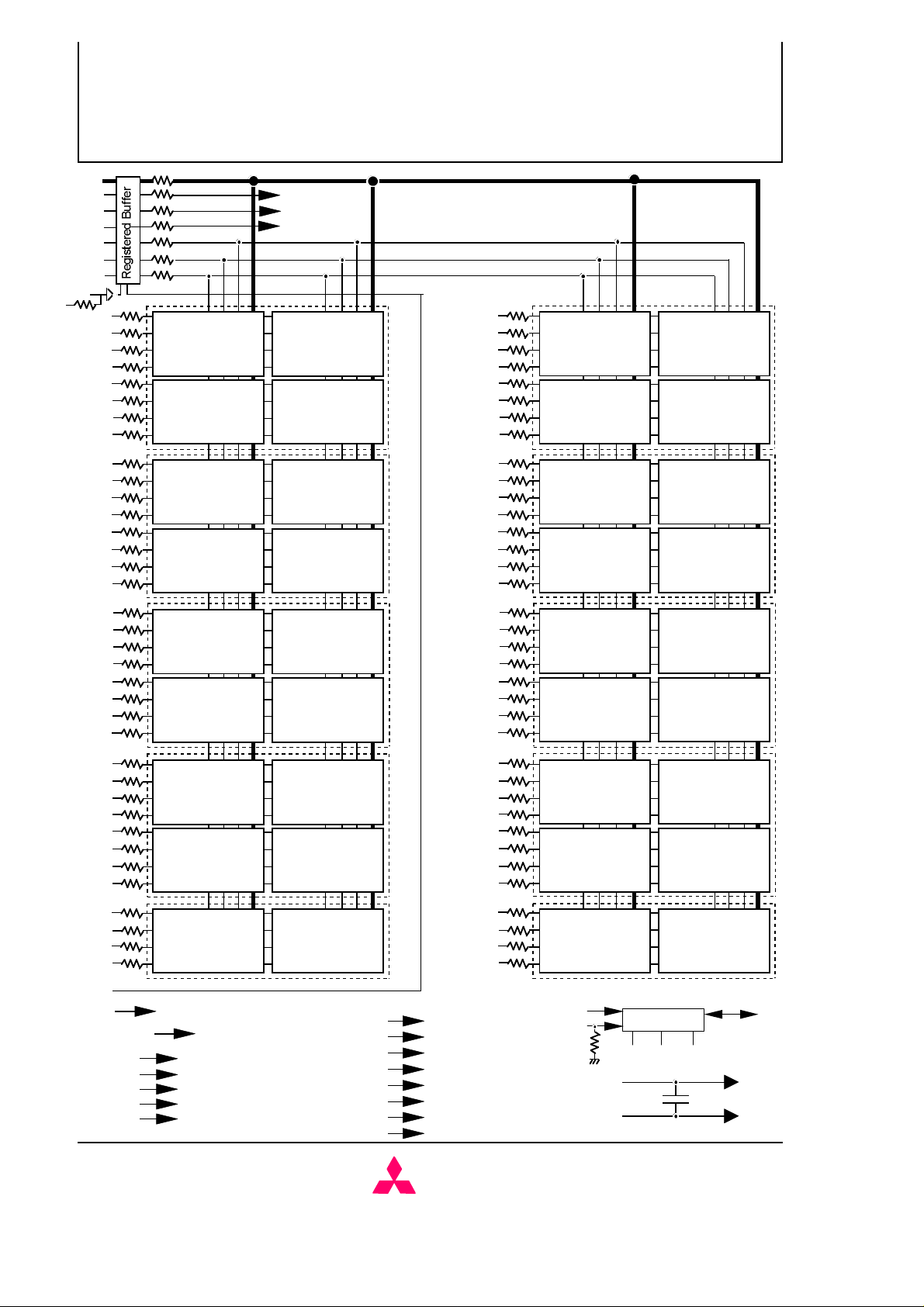
2,415,919,104-BIT ( 33,554,432-WORD BY 72-BIT ) Synchronous DYNAMIC RAM
The MH32S72DBFA is 33554432 - word x 72-bit
Synchronous DRAM stacked structural module. This
consist of thirty-six industry standard 16M x 4
Synchronous DRAMs in TSOP.
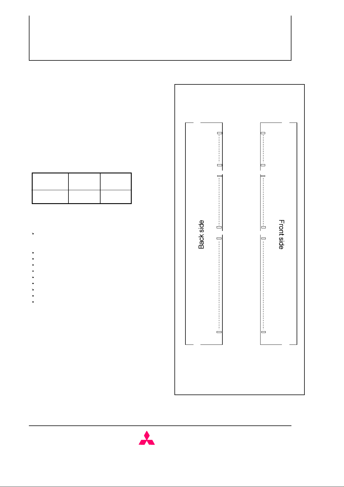
The stacked structure of TSOP on a card edge dual inline package provides any application where high
densities and large of quantities memory are required.
This is a socket-type memory module ,suitable for
easy interchange or addition of module.
MITSUBISHI LSIs
MH32S72DBFA -6
85pin
1pin
FEATURES
CLK
Max.
Utilizes industry standard 16M X 4 Synchronous DRAMs in
and industry standard PLL in TSSOP package.
Single 3.3V +/- 0.3V supply
Burst length 1/2/4/8/Full Page (programmable)
Burst type sequential / interleave (programmable)
Column access random
Burst Write / Single Write (programmable)
Auto precharge / Auto bank precharge controlled by A10
Auto refresh and Self refresh
LVTTL Interface
4096 refresh cycles every 64ms
APPLICATION
Main memory unit for computers, Microcomputer memory.
Access Time
[latch mode]
94pin
95pin
124pin
125pin
168pin
10pin
11pin
40pin
41pin
84pin
MIT-DS-352-0.0
MITSUBISHI
ELECTRIC
30/Sep. /1999
1
Page 2
Preliminary Spec.
Some contents are subject to change without notice.
MITSUBISHI LSIs
MH32S72DBFA -6
2,415,919,104-BIT ( 33,554,432-WORD BY 72-BIT ) Synchronous DYNAMIC RAM
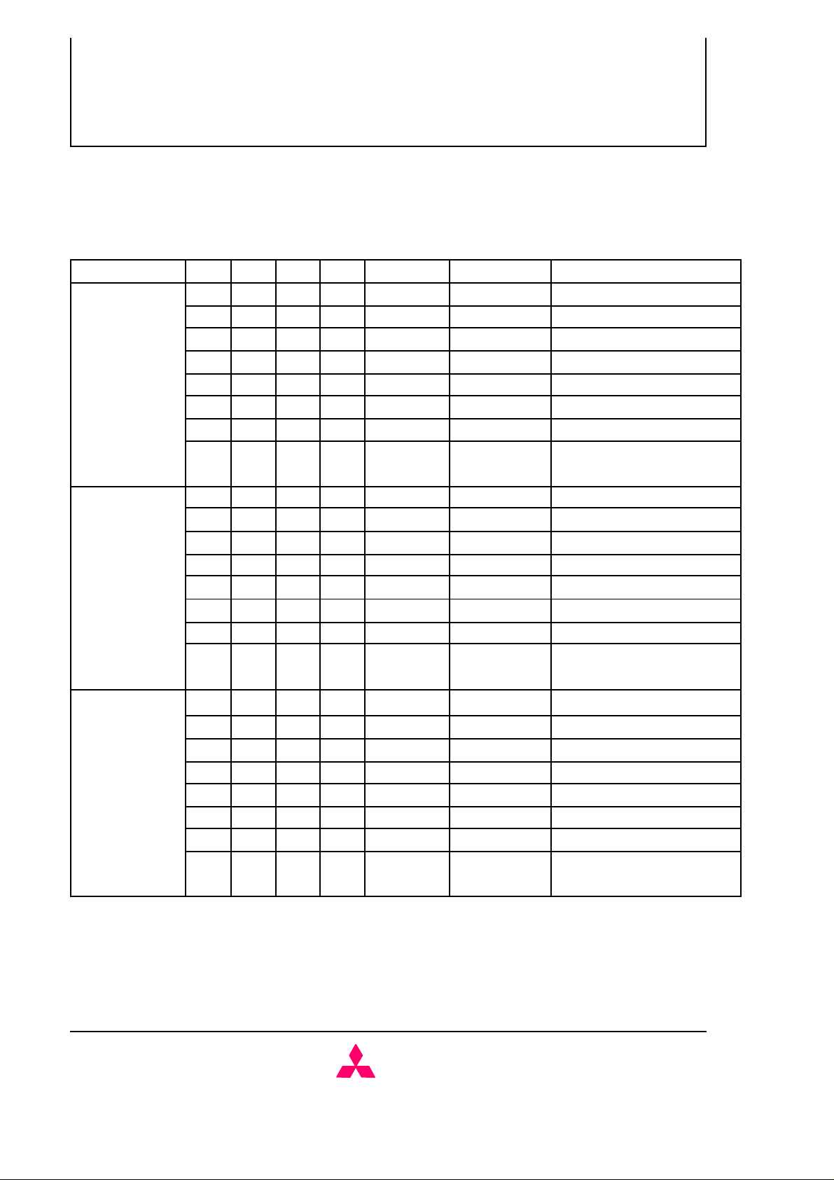
PIN NO. PIN NAME PIN NO. PIN NAME PIN NO. PIN NAME PIN NO. PIN NAME
1
2 DQ0 44 NC
3 DQ1 45 /S2
4 DQ2 46 DQMB2
5 DQ3 47 DQMB3
6 VDD 48 NC
7 DQ4 49 VDD
8 DQ5 50 NC
9 DQ6 51 NC
10 DQ7 52
11 DQ8 53
12
13 DQ9 55 DQ16
14 DQ10 56 DQ17
15 DQ11 57 DQ18
16 DQ12 58 DQ19
17 DQ13 59 VDD
18 VDD 60 DQ20
19 DQ14 61 NC
20 DQ15 62 NC
21
22
23 VSS 65 DQ21
24 NC 66 DQ22
25 NC 67 DQ23
26 VDD 68
27
28 DQMB0 70 DQ25
29 DQMB1 71 DQ26
30 /S0 72 DQ27
31 NC 73 VDD
32 VSS 74 DQ28
33 A0 75 DQ29
34 A2 76 DQ30
35 A4 77 DQ31
36 A6 78 VSS
37 A8 79
38
39
40 VDD 82 SDA
41 VDD 83 SCL
42 CK0 84 VDD
VSS
VSS
CB0
CB1
/WE0
A10
BA1
43
54 VSS
63
64 VSS
69 DQ24
80 NC
81
VSS 85
86
87
88
89
90
91
92
93
CB2
CB3
NC
VSS 110
CK2
WP
94
95
96
97
98
99
100
101
102
103
104
105
106
107
108
109
111
112
113
114
115
116
117
118
119
120
121
122
123
124
125
126
VSS 127
DQ32 128
DQ33 129
DQ34 130 DQMB6
DQ35 131 DQMB7
VDD 132
DQ36 133 VDD
DQ37 134 NC
DQ38 135 NC
DQ39 136
DQ40 137
VSS 138 VSS
DQ41 139 DQ48
DQ42 140 DQ49
DQ43 141 DQ50
DQ44 142 DQ51
DQ45 143 VDD
VDD 144 DQ52
DQ46 145 NC
DQ47 146
CB4
CB5
VSS 149 DQ53
NC 150 DQ54
NC 151 DQ55
VDD 152 VSS
/CAS 153 DQ56
DQMB4 154 DQ57
DQMB5 155 DQ58
/S1
/RAS 157 VDD
VSS 158 DQ60
A1 159 DQ61
A3 160 DQ62
A5 161 DQ63
A7 162 VSS
A9 163
BA0
A11
VDD 166 SA1
CK1 167 SA2
NC
147
148 VSS
156 DQ59
164 NC
165 SA0
168 VDD
VSS
CKE0
/S3
NC
CB6
CB7
NC
REGE
CK3
NC = No Connection
MIT-DS-352-0.0
MITSUBISHI
ELECTRIC
30/Sep. /1999
2
Page 3
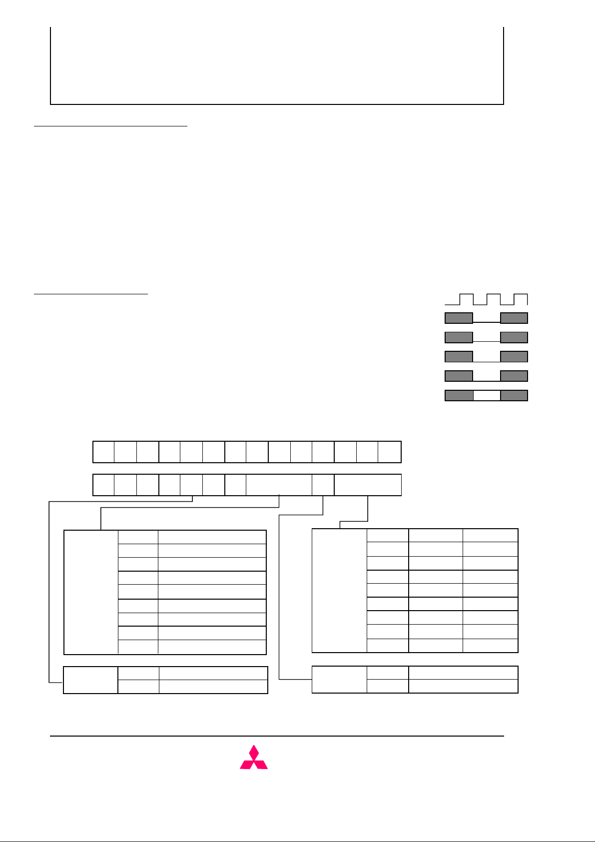
Add
D18
D19D0D1
D2
D20
D3
D21D4D22
D5
D23
D6
D24
D7
D25D8D26D9D27
D10
D28
D11
D29
D12
D30
D13
D31
D14
D32
D15
D33
D16
D34
D17
D35
47K
CKE0
/S0-3
DQM0-7
/W
/RAS
/CAS
REGE
Vdd
DQ0
DQ1
DQ2
DQ3
DQ4
DQ5
DQ6
DQ7
Preliminary Spec.
Some contents are subject to change without notice.
2,415,919,104-BIT ( 33,554,432-WORD BY 72-BIT ) Synchronous DYNAMIC RAM
RCKE0
R/S0-3
RDQM0-7
MITSUBISHI LSIs
MH32S72DBFA -6
DQ32
DQ33
DQ34
DQ35
DQ36
DQ37
DQ38
DQ39
DQ8
DQ9
DQ10
DQ11
DQ12
DQ13
DQ14
DQ15
DQ16
DQ17
DQ18
DQ19
DQ20
DQ21
DQ22
DQ23
DQ24
DQ25
DQ26
DQ27
DQ28
DQ29
DQ30
DQ31
CB0
CB1
CB2
CB3
From PLL
CK0
CK1 - CK3 Terminated
RCKE0
R/S0
R/S1
R/S2
R/S3
PLL
D0-35
D0-3,D8-12,D17
D18-21,D26-30,D35
D4-7,D13-16
D22-25,D31-34
RDQM 0
RDQM 1
RDQM 2
RDQM 3
RDQM 4
RDQM 5
RDQM 6
RDQM 7
DQ40
DQ41
DQ42
DQ43
DQ44
DQ45
DQ46
DQ47
DQ48
DQ49
DQ50
DQ51
DQ52
DQ53
DQ54
DQ55
DQ56
DQ57
DQ58
DQ59
DQ60
DQ61
DQ62
DQ63
CB4
CB5
CB6
CB7
D0-1,D18-19
D2-3,D8,D20-21,D26
SCL
WP
D4-5,D22-23
D6-7,D24-25
D9-10,D27-28
D11-12,D17,D29-30,D35
D13-14,D31-32
D15-16,D33-34
SERIAL PD
A0 A1 A2
SA0 SA1 SA2
VDD
VSS
SDA
D0 to D35
D0 to D35
MIT-DS-352-0.0
MITSUBISHI
ELECTRIC
30/Sep. /1999
3
Page 4
Preliminary Spec.
PIN FUNCTION
the bank to which a command is applied.BA must be set
Register enable:When REGE is low,All control signals and
Some contents are subject to change without notice.
2,415,919,104-BIT ( 33,554,432-WORD BY 72-BIT ) Synchronous DYNAMIC RAM
MITSUBISHI LSIs
MH32S72DBFA -6
CK0
CKE0
/S0 - 3
/RAS,/CAS,/W
A0-11
BA0-1
Input
Input
Input
Input
Input
Input
Master Clock:All other inputs are referenced to the rising
edge of CK
Clock Enable:CKE controls internal clock.When CKE is
low,internal clock for the following cycle is ceased. CKE is
also used to select auto / self refresh. After self refresh
mode is started, CKE E becomes asynchronous input.Self
refresh is maintained as long as CKE is low.
Chip Select: When /S is high,any command means
No Operation.
Combination of /RAS,/CAS,/W defines basic commands.
A0-11 specify the Row/Column Address in conjunction with
BA.The Row Address is specified by A0-11.The Column
Address is specified by A0-9.A10 is also used to indicate
precharge option.When A10 is high at a read / write
command, an auto precharge is performed. When A10 is
high at a precharge command, both banks are precharged.
Bank Address:BA0,1 is not simply BA.BA0,1 specifies
with ACT,PRE,READ,WRITE commands
DQ0-63
CB0-7
DQM0-7
Vdd,Vss
REGE
MIT-DS-352-0.0
Input/Output
Input
Power Supply
Output
Data In and Data out are referenced to the rising edge
of CK
Din Mask/Output Disable:When DQMB is high in burst
write.Din for the current cycle is masked.When DQMB is
high in burst read,Dout is disabled at the next but one cycle.
Power Supply for the memory mounted module.
address are buffered. (Buffer mode) When REGE is
high,All control and address are latched. (Latch mode)
MITSUBISHI
ELECTRIC
30/Sep. /1999
4
Page 5
Preliminary Spec.
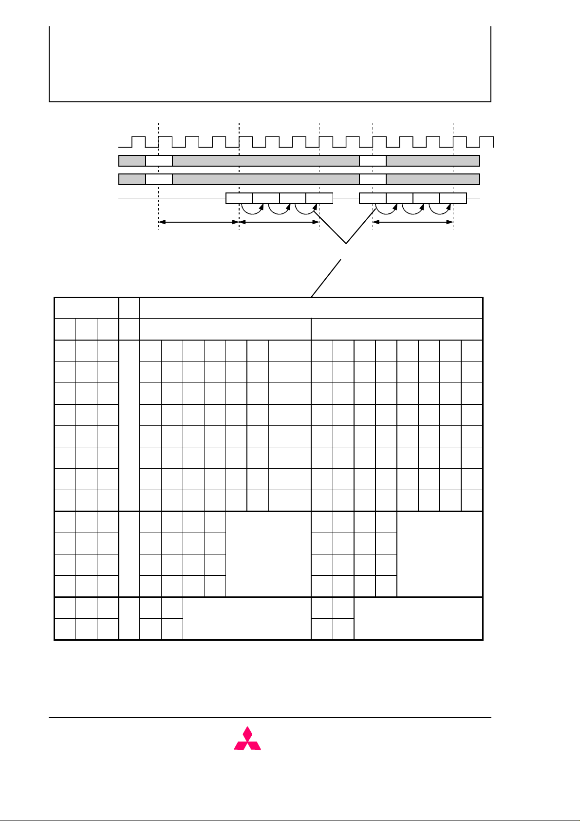
BASIC FUNCTIONS
Each command is defined by control signals of /RAS,/CAS and /WE at CK rising edge. In
READ command starts burst read from the active bank indicated by BA.First output
Some contents are subject to change without notice.
MITSUBISHI LSIs
MH32S72DBFA -6
2,415,919,104-BIT ( 33,554,432-WORD BY 72-BIT ) Synchronous DYNAMIC RAM
The MH32S72DBFA provides basic functions,bank(row)activate,burst read / write,
bank(row)precharge,and auto / self refresh.
addition to 3 signals,/S,CKE and A10 are used as chip select,refresh option,and
precharge option,respectively.
To know the detailed definition of commands please see the command truth table.
CK
/S
/RAS
/CAS
/WE
CKE
A10
Chip Select : L=select, H=deselect
Command
Command
Command
Refresh Option @refresh command
Precharge Option @precharge or read/write command
define basic commands
Activate(ACT) [/RAS =L, /CAS = /WE =H]
ACT command activates a row in an idle bank indicated by BA.
Read(READ) [/RAS =H,/CAS =L, /WE =H]
data appears after /CAS latency. When A10 =H at this command,the bank is
deactivated after the burst read(auto-precharge,READA).
Write(WRITE) [/RAS =H, /CAS = /WE =L]
WRITE command starts burst write to the active bank indicated by BA. Total data
length to be written is set by burst length. When A10 =H at this command, the bank
is deactivated after the burst write(auto-precharge,WRITEA).
Precharge(PRE) [/RAS =L, /CAS =H,/WE =L]
PRE command deactivates the active bank indicated by BA. This command also
terminates burst read / write operation. When A10 =H at this command, both banks
are deactivated(precharge all, PREA).
Auto-Refresh(REFA) [/RAS =/CAS =L, /WE =CKE =H]
PEFA command starts auto-refresh cycle. Refresh address including bank address
are generated internally. After this command, the banks are precharged automatically.
MIT-DS-352-0.0
MITSUBISHI
30/Sep. /1999
ELECTRIC
5
Page 6
Preliminary Spec.
Some contents are subject to change without notice.
2,415,919,104-BIT ( 33,554,432-WORD BY 72-BIT ) Synchronous DYNAMIC RAM
COMMAND TRUTH TABLE
MITSUBISHI LSIs
MH32S72DBFA -6
COMMAND
Deselect
No Operation
Row Address Entry &
Bank Activate
Single Bank Precharge
Precharge All Banks
Column Address Entry
& Write
Column Address Entry
& Write with Auto-
Precharge
Column Address Entry
& Read
Column Address Entry
& Read with Auto-
Precharge
Auto-Refresh
Self-Refresh Entry
Self-Refresh Exit
Burst Terminate
Mode Register Set
MNEMONIC
DESEL
NOP
ACT
PRE
PREA
WRITE
WRITEA
READ
READA
REFA
REFS
REFSX
TBST
MRS
CKE
n-1
H
H
H
H
H
H
H
H
H
H
H
L
L
H
H
CKE
n
X
X
X
X
X
X
X
X
X
H
L
H
H
X
X
/CS
H
L
L
L
L
L
L
L
L
L
L
H
L
L
L
/RAS
X
H
L
L
L
H
H
H
H
L
L
X
H
H
L
/CAS
X
H
H
H
H
L
L
L
L
L
L
X
H
H
L
/WE
X
H
H
L
L
L
L
H
H
H
H
X
H
L
L
BA0,1
X
X
V
V
X
V
V
V
V
X
X
X
X
X
L
A11
X
X
V
X
X
X
X
X
X
X
X
X
X
X
L
A10
X
X
V
L
H
L
H
L
H
X
X
X
X
X
L
A0-9
X
X
V
X
X
V
V
V
V
X
X
X
X
X
V*1
H=High Level, L=Low Level, V=Valid, X=Don't Care, n=CLK cycle number
NOTE:
1. A7-A9 =0, A0-A6 =Mode Address
MIT-DS-352-0.0
MITSUBISHI
ELECTRIC
30/Sep. /1999
6
Page 7
Preliminary Spec.
Some contents are subject to change without notice.
2,415,919,104-BIT ( 33,554,432-WORD BY 72-BIT ) Synchronous DYNAMIC RAM
FUNCTION TRUTH TABLE
MITSUBISHI LSIs
MH32S72DBFA -6
Current State
IDLE
ROW ACTIVE
READ
/S
/RAS
H
L
L
L
L
L
L
L
H
L
L
L
L
L
L
L
L
H
L
L
L
L
L
L
L
L
/CAS
X
H
H
H
L
L
L
L
X
H
H
H
H
L
L
L
L
X
H
H
H
H
L
L
L
L
/WE
X
H
H
L
H
H
L
L
X
H
H
L
L
H
H
L
L
X
H
H
L
L
H
H
L
L
X
H
L
X
H
L
H
L
X
H
L
H
L
H
L
H
L
X
H
L
H
L
H
L
H
L
Address
X
X
BA
BA,CA,A10
BA,RA
BA,A10
X
Op-Code,
Mode-Add
X
X
BA
BA,CA,A10
BA,CA,A10
BA,RA
BA,A10
X
Op-Code,
Mode-Add
X
X
BA
BA,CA,A10
BA,CA,A10
BA,RA
BA,A10
X
Op-Code,
Mode-Add
Command
DESEL
NOP
TBST
READ/WRITE
ACT
PRE/PREA
REFA
MRS
DESEL
NOP
TBST
READ/READA
WRITE/
WRITEA
ACT
PRE/PREA
REFA
MRS
DESEL
NOP
TBST
READ/READA
WRITE/WRITEA
ACT
PRE/PREA
REFA
MRS
Action
NOP
NOP
ILLEGAL*2
ILLEGAL*2
Bank Active,Latch RA
NOP*4
Auto-Refresh*5
Mode Register Set*5
NOP
NOP
NOP
Begin Read,Latch CA,
Determine Auto-Precharge
Begin Write,Latch CA,
Determine Auto-Precharge
Bank Active/ILLEGAL*2
Precharge/Precharge All
ILLEGAL
ILLEGAL
NOP(Continue Burst to END)
NOP(Continue Burst to END)
Terminate Burst
Terminate Burst,Latch CA,
Begin New Read,Determine
Auto-Precharge*3
Terminate Burst,Latch CA,
Begin Write,Determine AutoPrecharge*3
Bank Active/ILLEGAL*2
Terminate Burst,Precharge
ILLEGAL
ILLEGAL
MIT-DS-352-0.0
MITSUBISHI
ELECTRIC
30/Sep. /1999
7
Page 8
Preliminary Spec.
FUNCTION TRUTH TABLE
(continued)
Some contents are subject to change without notice.
2,415,919,104-BIT ( 33,554,432-WORD BY 72-BIT ) Synchronous DYNAMIC RAM
MITSUBISHI LSIs
MH32S72DBFA -6
Current State
WRITE
READ with
AUTO
PRECHARGE
WRITE with
AUTO
PRECHARGE L
/S
/RAS
H
L
L
L
L
L
L
L
L
H
L
L
L
L
L
L
L
L
H
L
L
L
L
L
L
L
/CAS
X
H
H
H
H
L
L
L
L
X
H
H
H
H
L
L
L
L
X
H
H
H
H
L
L
L
L
/WE
X
H
H
L
L
H
H
L
L
X
H
H
L
L
H
H
L
L
X
H
H
L
L
H
H
L
L
X
H
L
H
L
H
L
H
L
X
H
L
H
L
H
L
H
L
X
H
L
H
L
H
L
H
L
Address
X
X
BA
BA,CA,A10
BA,CA,A10
BA,RA
BA,A10
X
Op-Code,
Mode-Add
X
X
BA
BA,CA,A10
BA,CA,A10
BA,RA
BA,A10
X
Op-Code,
Mode-Add
X
X
BA
BA,CA,A10
BA,CA,A10
BA,RA
BA,A10
X
Op-Code,
Mode-Add
Command
DESEL
NOP
TBST
READ/READA
WRITE/
WRITEA
ACT
PRE/PREA
REFA
MRS
DESEL
NOP
TBST
READ/READA
WRITE/
WRITEA
ACT
PRE/PREA
REFA
MRS
DESEL
NOP
TBST
READ/READA
WRITE/
WRITEA
ACT
PRE/PREA
REFA
MRS
Action
NOP(Continue Burst to END)
NOP(Continue Burst to END)
Terminate Burst
Terminate Burst,Latch CA,
Begin Read,Determine Auto-
Precharge*3
Terminate Burst,Latch CA,
Begin Write,Determine AutoPrecharge*3
Bank Active/ILLEGAL*2
Terminate Burst,Precharge
ILLEGAL
ILLEGAL
NOP(Continue Burst to END)
NOP(Continue Burst to END)
ILLEGAL
ILLEGAL
ILLEGAL
Bank Active/ILLEGAL*2
ILLEGAL*2
ILLEGAL
ILLEGAL
NOP(Continue Burst to END)
NOP(Continue Burst to END)
ILLEGAL
ILLEGAL
ILLEGAL
Bank Active/ILLEGAL*2
ILLEGAL*2
ILLEGAL
ILLEGAL
MIT-DS-352-0.0
MITSUBISHI
ELECTRIC
30/Sep. /1999
8
Page 9
Preliminary Spec.
Some contents are subject to change without notice.
MH32S72DBFA -6
2,415,919,104-BIT ( 33,554,432-WORD BY 72-BIT ) Synchronous DYNAMIC RAM
FUNCTION TRUTH TABLE(continued)
MITSUBISHI LSIs
Current State
PRE -
CHARGING
ROW
ACTIVATING
/S
H
L
L
L
L
L
L
L
H
L
L
L
L
L
L
L
/RAS
X
H
H
H
L
L
L
L
X
H
H
H
L
L
L
L
/CAS
X
H
H
L
H
H
L
L
X
H
H
L
H
H
L
L
/WE
X
H
L
X
H
L
H
L
X
H
L
X
H
L
H
L
Address
X
X
BA
BA,CA,A10
BA,RA
BA,A10
X
Op-Code,
Mode-Add
X
X
BA
BA,CA,A10
BA,RA
BA,A10
X
Op-Code,
Mode-Add
Command
DESEL
NOP
TBST
READ/WRITE
ACT
PRE/PREA
REFA
MRS
DESEL
NOP
TBST
READ/WRITE
ACT
PRE/PREA
REFA
MRS
Action
NOP(Idle after tRP)
NOP(Idle after tRP)
ILLEGAL*2
ILLEGAL*2
ILLEGAL*2
NOP*4(Idle after tRP)
ILLEGAL
ILLEGAL
NOP(Row Active after tRCD
NOP(Row Active after tRCD
ILLEGAL*2
ILLEGAL*2
ILLEGAL*2
ILLEGAL*2
ILLEGAL
ILLEGAL
WRITE RE-
COVERING
MIT-DS-352-0.0
H
L
L
L
L
L
L
L
X
H
H
H
L
L
L
L
X
H
H
L
H
H
L
L
X
H
L
X
H
L
H
L
X
X
BA
BA,CA,A10
BA,RA
BA,A10
X
Mode-Add
Op-Code,
MITSUBISHI
DESEL
NOP
TBST
READ/WRITE
ACT
PRE/PREA
REFA
MRS
NOP
NOP
ILLEGAL*2
ILLEGAL*2
ILLEGAL*2
ILLEGAL*2
ILLEGAL
ILLEGAL
30/Sep. /1999
9
ELECTRIC
Page 10
Preliminary Spec.
1. All entries assume that CKE was High during the preceding clock cycle and the current
Some contents are subject to change without notice.
MH32S72DBFA -6
2,415,919,104-BIT ( 33,554,432-WORD BY 72-BIT ) Synchronous DYNAMIC RAM
FUNCTION TRUTH TABLE(continued)
MITSUBISHI LSIs
Current State
RE-
FRESHING
MODE
REGISTER
SETTING
/S
H
L
L
L
L
L
L
L
H
L
L
L
L
L
L
/RAS
X
H
H
H
L
L
L
L
X
H
H
H
L
L
L
/CAS
X
H
H
L
H
H
L
L
X
H
H
L
H
H
L
/WE
X
H
L
X
H
L
H
L
X
H
L
X
H
L
H
Address
X
X
BA
BA,CA,A10
BA,RA
BA,A10
X
Op-Code,
Mode-Add
X
X
BA
BA,CA,A10
BA,RA
BA,A10
X
Command
DESEL
NOP NOP(Idle after tRC)
TBST
READ/WRITE
ACT
PRE/PREA
REFA
MRS
DESEL
NOP
TBST
READ/WRITE
ACT
PRE/PREA
REFA
NOP(Idle after tRC)
ILLEGAL
ILLEGAL
ILLEGAL
ILLEGAL
ILLEGAL
ILLEGAL
NOP(Idle after tRSC)
NOP(Idle after tRSC)
ILLEGAL
ILLEGAL
ILLEGAL
ILLEGAL
ILLEGAL
Action
L
L
L
L
Op-Code,
Mode-Add
MRS
ILLEGAL
ABBREVIATIONS:
H = Hige Level, L = Low Level, X = Don't Care
BA = Bank Address, RA = Row Address, CA = Column Address, NOP = No Operation
NOTES:
clock cycle.
2. ILLEGAL to bank in specified state; function may be legal in the bank indicated by BA,
depending on the state of that bank.
3. Must satisfy bus contention, bus turn around, write recovery requirements.
4. NOP to bank precharging or in idle state.May precharge bank indicated by BA.
5. ILLEGAL if any bank is not idle.
ILLEGAL = Device operation and / or date-integrity are not guaranteed.
MIT-DS-352-0.0
MITSUBISHI
30/Sep. /1999
ELECTRIC
10
Page 11
Preliminary Spec.
2. Power-Down and Self-Refresh can be entered only form the All banks idle State.
Some contents are subject to change without notice.
MH32S72DBFA -6
2,415,919,104-BIT ( 33,554,432-WORD BY 72-BIT ) Synchronous DYNAMIC RAM
FUNCTION TRUTH TABLE FOR CKE
MITSUBISHI LSIs
Current State
SELF -
REFRESH*1
POWER
DOWN
ALL BANKS
IDLE*2
ANY STATE
other than
listed above
CK
n-1
CK
n
H
L
L
L
L
L
L
H
L
L
H
H
H
H
H
H
H
L
H
H
L
L
X
H
H
H
H
H
L
X
H
L
H
L
L
L
L
L
L
X
H
L
H
L
/S
X
H
L
L
L
L
X
X
X
X
X
L
H
L
L
L
L
X
X
X
X
X
/RAS
X
X
H
H
H
L
X
X
X
X
X
L
X
H
H
H
L
X
X
X
X
X
/CAS
X
X
H
H
L
X
X
X
X
X
X
L
X
H
H
L
X
X
X
X
X
X
/WE
X
X
H
L
X
X
X
X
X
X
X
H
X
H
L
X
X
X
X
X
X
X
Add
X
INVALID
Exit Self-Refresh(Idle after tRC)
X
Exit Self-Refresh(Idle after tRC)
X
ILLEGAL
X
ILLEGAL
X
ILLEGAL
X
NOP(Maintain Self-Refresh)
X
X
INVALID
Exit Power Down to Idle
X
NOP(Maintain Self-Refresh)
X
X
Refer to Function Truth Table
Enter Self-Refresh
X
Enter Power Down
X
Enter Power Down
X
ILLEGAL
X
ILLEGAL
X
ILLEGAL
X
Refer to Current State = Power Down
X
X
Refer to Function Truth Table
Begin CK0 Suspend at Next Cycle*3
X
X
Exit CK0 Suspend at Next Cycle*3
X
Maintain CK0 Suspend
Action
ABBREVIATIONS:
H = High Level, L = Low Level, X = Don't Care
NOTES:
1. CKE Low to High transition will re-enable CK and other inputs asynchronously.
A minimum setup time must be satisfied before any command other than EXIT.
3. Must be legal command.
MIT-DS-352-0.0
MITSUBISHI
ELECTRIC
30/Sep. /1999
11
Page 12
Preliminary Spec.
POWER ON SEQUENCE
After these sequence, the SDRAM is idle state and ready for normal operation.
MODE REGISTER
LENGTH
BURST
Some contents are subject to change without notice.
MITSUBISHI LSIs
MH32S72DBFA -6
2,415,919,104-BIT ( 33,554,432-WORD BY 72-BIT ) Synchronous DYNAMIC RAM
Before starting normal operation, the following power on sequence is necessary to prevent
a SDRAM from damaged or malfunctioning.
1. Apply power and start clock. Attempt to maintain CKE high, DQMB high and NOP
condition at the inputs.
2. Maintain stable power, stable cock, and NOP input conditions for a minimum of 500µs.
3. Issue precharge commands for all banks. (PRE or PREA)
4. After all banks become idle state (after tRP), issue 8 or more auto-refresh commands.
5. Issue a mode register set command to initialize the mode register.
Burst Length, Burst Type and /CAS Latency can be
programmed by setting the mode register(MRS). The mode
register stores these date until the next MRS command, which
may be issue when both banks are in idle state. After tRSC
from a MRS command, the SDRAM is ready for new command.
BA0
0
LATENCY
MODE
BA1
0
0 0 0
0 0 1
0 1 0
0 1 1
1 0 0
1 0 1
1 1 0
1 1 1
A11
0
CL
A9
A10
0
/CAS LATENCY
WM
A8
0
R
R
2
3
R
R
R
R
A7
0
A5
A6
LTMODE
A4
A3
BT
BURST
A2
BL
BA0,1 A11-A0
A1
A0
BL
0 0 0
0 0 1
0 1 0
0 1 1
1 0 0
1 0 1
1 1 0
1 1 1
CLK
/CS
/RAS
/CAS
/WE
BT= 0
1
2
4
8
R
R
R
FP
V
BT= 1
1
2
4
8
R
R
R
R
WRITE
MODE
MIT-DS-352-0.0
0
1
BURST
SINGLE BIT
TYPE
MITSUBISHI
0
1
R: Reserved for Future Use
FP: Full Page
ELECTRIC
SEQUENTIAL
INTERLEAVED
30/Sep. /1999
12
Page 13
Preliminary Spec.
Some contents are subject to change without notice.
2,415,919,104-BIT ( 33,554,432-WORD BY 72-BIT ) Synchronous DYNAMIC RAM
CK
MITSUBISHI LSIs
MH32S72DBFA -6
Command
Address
DQ
CL= 3
BL= 4
Initial Address BL
A2
0
0
0
0
1
A1
0
0
1
1
0
A0
0
1
0
1
8
0
Read
Y
/CAS Latency
1
0
2
1
3
2
4
3
5
4
Sequential
3
2
4
3
5
4
6
5
7
6
Q0 Q1 Q2 Q3
Burst Length
Column Addressing
5
4
6
5
7
6
0
7
1
0
7
6
0
7
1
0
2
1
3
2
Burst Type
1
0
0
1
3
2
2
3
5
4
Write
Y
D0 D1
Burst Length
Interleaved
3
2
2
3
1
0
0
1
7
6
D3
D2
5
4
4
5
7
6
6
7
1
0
7
6
6
7
5
4
4
5
3
2
0
1
1
1
-
-
-
-
-
-
MIT-DS-352-0.0
1
0
1
1
1
0
0
0
1
0
1
1
1
0
-
-
1
6
5
7
6
0
7
1
0
2
1
4
3
2
0
3
1
0
2
1
0
0
7
1
0
2
1
3
2
0
3
1
0
1
2
2
1
3
2
3
4
MITSUBISHI
4
3
5
4
5
6
4
5
7
6
6
7
1
0
0
1
3
2
2
3
1
0
1
0
6
7
5
4
4
5
3
2
2
3
1
0
1
0
0
1
3
2
3
2
2
3
1
0
1
0
30/Sep. /1999
13
ELECTRIC
Page 14
Preliminary Spec.
ABSOLUTE MAXIMUM RATINGS
mA
RECOMMENDED OPERATING CONDITION
CAPACITANCE
Some contents are subject to change without notice.
2,415,919,104-BIT ( 33,554,432-WORD BY 72-BIT ) Synchronous DYNAMIC RAM
MITSUBISHI LSIs
MH32S72DBFA -6
Symbol
Vdd
VI
VO
IO
Pd
Topr
Tstg
Operating Temperature
Parameter
Supply Voltage
Input Voltage
Output Voltage
Output Current
Power Dissipation
Storage Temperature
(Ta=0 ~ 70°C, unless otherwise noted)
Symbol
Vdd
Parameter
Supply Voltage
Condition
with respect to Vss
with respect to Vss
with respect to Vss
Ta=25°C
Min.
3.0
Limits
Typ.
3.3
Ratings
-0.5 ~ 4.6
-0.5 ~ 4.6
-0.5 ~ 4.6
50
39
0 ~ 70
-40 ~ 100
Max.
3.6
Unit
V
V
V
W
°C
°C
Unit
V
Vss
VIH
VIL
Note)
1:VIH(max)=5.5V for pulse width less than 10ns.
2.VIL(min)=-1.0 for pulse width less than 10ns.
High-Level Input Voltage all inputs
Low-Level Input Voltage all inputs
Supply Voltage
0
2.0
-0.3
0
(Ta=0 ~ 70°C, Vdd = 3.3 +/- 0.3V, Vss = 0V, unless otherwise noted)
Symbol
CI(A)
Input Capacitance, address pin
CI(C)
CI(CK)
CI(K)
CI/O
MIT-DS-352-0.0
Parameter
Input Capacitance, control pin
Input Capacitance, CKE pin
Input Capacitance, CK pin
Input Capacitance, I/O pin
Test Condition
1MHz,
1.4V bias
200mV swing
MITSUBISHI
Limits(max.)
ELECTRIC
Vdd+0.3
25
25
50
50
29
0
0.8
Unit
pF
pF
pF
pF
pF
30/Sep. /1999
V
V
V
14
Page 15
Preliminary Spec.
AVERAGE SUPPLY CURRENT from Vdd
AC OPERATING CONDITIONS AND CHARACTERISTICS
Limits
(max)
precharge stanby
in power-down mode
precharge stanby current
in non power-down mode
active stanby current
one bank active (discrete)
Some contents are subject to change without notice.
MITSUBISHI LSIs
MH32S72DBFA -6
2,415,919,104-BIT ( 33,554,432-WORD BY 72-BIT ) Synchronous DYNAMIC RAM
(Ta=0 ~70°C, Vdd = 3.3 ± 0.3V, Vss = 0V, unless otherwise noted)
Parameter
operating current
one bank active (discrete)
current
in non power-down mode
burst current
auto-refresh current
self-refresh current
Note)
1.Icc(max) is specified at the output open condition.
2.Input signals are changed one time during 30ns.
Symbol
Icc1
Icc2P
Icc2PS
Icc2N
Icc2NS
Icc3N
Icc3NS
Icc4
Icc5
Icc6
tRC=min.tCLK=min, BL=1,CL=3
CKE=L,tCLK=15ns, /CS>Vcc-0.2V
CKE=CLK=L, /CS>Vcc-0.2V
CKE=H,tCLK=15ns,VIH>Vcc-0.2V,VIL<0.2V
CKE=H,CLK=L,VIH>Vcc-0.2V,VIL<0.2V(fixed)
CKE=H,tCLK=15ns
CKE=H,CLK=L
tCLK=min, BL=4, CL=3,all banks active(discerte)
tRC=min, tCLK=min
CKE <0.2V
Test Condition
(Ta=0 ~ 70°C, Vdd = 3.3 ± 0.3V, Vss = 0V, unless otherwise noted)
Symbol
VOH(DC)
VOL(DC)
IOZ
Ii
Parameter
High-Level Output Voltage(DC)
Low-Level Output Voltage(DC)
Off-stare Output Current
Input Current
Test Condition
IOH=-2mA
IOL=2mA
Q floating VO=0 ~ Vdd
VIH=0 ~ Vdd+0.3V
Limits
Min.
2.4
-10
-10
Max.
0.4
10
10
Unit
V
V
uA
uA
-6
1925
107
71
755
575
1115
935
2195
4715
71
Unit
mA
mA
mA
mA
mA
mA
mA
mA
mA
mA
MIT-DS-352-0.0
MITSUBISHI
ELECTRIC
30/Sep. /1999
15
Page 16
Preliminary Spec.
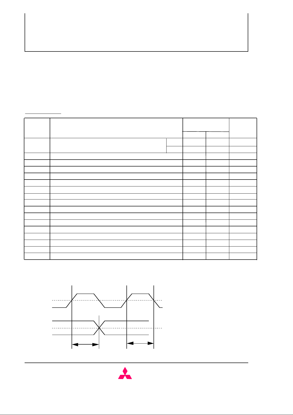
AC TIMING REQUIREMENTS
Parameter
Self Refresh Exit time
Note:1 The timing requirements are assumed tT=1ns.If tT is longer than 1ns,(tT-1)ns
should be added to the parameter.
Some contents are subject to change without notice.
MITSUBISHI LSIs
MH32S72DBFA -6
2,415,919,104-BIT ( 33,554,432-WORD BY 72-BIT ) Synchronous DYNAMIC RAM
(Ta=0 ~ 70C, Vdd = 3.3 +/- 0.3V, Vss = 0V, unless otherwise noted)
Input Pulse Levels: 0.8V to 2.0V
Input Timing Measurement Level: 1.4V
LATCH MODE
Symbol
tCLK CK cycle time
tCH CK High pulse width
tCL CK Low pulse width
tT Transition time of CK
tIS Input Setup time(all inputs)
tIH Input Hold time(all inputs)
tRC Row Cycle time
tRFC Row Refresh Cycle time
tRCD Row to Column Delay
tRAS Row Active time
tRP Row Precharge time
tWR
Write Recovery time
tRRD Act to Act Deley time
tRSC Mode Register Set Cycle time
tSRX
tPDE Power Down Exit time
tREF Refresh Interval time
CL=3
CL=4 7.5 ns
Min. Max.
10
2.5
2.5
1
1.5
0.8
67.5
75
20
45
20
15
15
10
7.5
7.5
Limits
10
100K
64
Unit
ns
ns
ns
ns
ns
ns
ns
ns
ns
ns
ns
ns
ns
ns
ns
ns
ms
CK
1.4V
Any AC timing is
referenced to the input
signal crossing
Signal
MIT-DS-352-0.0
1.4V
MITSUBISHI
through 1.4V.
30/Sep. /1999
ELECTRIC
16
Page 17
Preliminary Spec.
SWITCHING CHARACTERISTICS
Parameter
Output Hold time
Parameter
Self Refresh Exit time
Note:1 The timing requirements are assumed tT=1ns.If tT is longer than 1ns,(tT-1)ns
should be added to the parameter.
Some contents are subject to change without notice.
MITSUBISHI LSIs
MH32S72DBFA -6
2,415,919,104-BIT ( 33,554,432-WORD BY 72-BIT ) Synchronous DYNAMIC RAM
BUFFER MODE
Limits
Symbol
CL=2
tCLK CK cycle time
CL=3 ns
tCH CK High pulse width ns
tCL CK Low pulse width
tT Transition time of CK
tIS Input Setup time(all inputs)
tIH Input Hold time(all inputs) ns
tRC Row Cycle time
tRFC Row Refresh Cycle time
tRCD Row to Column Delay
tRAS Row Active time
tRP Row Precharge time
tWR
Write Recovery time
tRRD Act to Act Deley time
tRSC Mode Register Set Cycle time
tSRX
tPDE Power Down Exit time
tREF Refresh Interval time
Min. Max.
10
7.5
2.5
2.5
1
6.5
0
67.5
75
20
45
20
15
15
10
7.5
7.5
10
100K
64
Unit
ns
ns
ns
ns
ns
ns
ns
ns
ns
ns
ns
ns
ns
ns
ms
(Ta=0 ~ 70C, Vdd = 3.3 +/- 0.3V, Vss = 0V, unless otherwise noted)
LATCH MODE
Limits
Symbol
Unit
Min. Max.
6
ns
5.4
ns
tAC Access time from CK
tOH
from CK
CL=3
CL=4
CL=3
CL=4
3
2.7
Delay time, output low
tOLZ
tOHZ
impedance from CK
Delay time, output high
impedance from CK
0
2.7 5.4
ns
ns
NOTE)
1.If clock rising time is longer than 1ns, (tr /2-0.5ns) should be added to the parameter.
MIT-DS-352-0.0
MITSUBISHI
30/Sep. /1999
ELECTRIC
17
Page 18

Preliminary Spec.
Parameter
Output Hold time
Some contents are subject to change without notice.
2,415,919,104-BIT ( 33,554,432-WORD BY 72-BIT ) Synchronous DYNAMIC RAM
BUFFER MODE
MITSUBISHI LSIs
MH32S72DBFA -6
Symbol
Limits
Min. Max.
CL=2
6
tAC Access time from CK
tOH
from CK
CL=3
CL=2
CL=3
3
2.7
5.4
Delay time, output low
tOLZ
tOHZ
impedance from CK
Delay time, output high
impedance from CK
0
2.7 5.4
NOTE)
1.If clock rising time is longer than 1ns, (tr /2-0.5ns) should be added to the parameter.
Output Load Condition
CK
Unit
ns
ns
ns
ns
1.4V
VOUT
MIT-DS-352-0.0
Ext.CL=50pF
CK
tAC tOH
Output Timing
Measurement
Reference Point
tOHZ
MITSUBISHI
ELECTRIC
DQ
1.4V
1.4VDQ
30/Sep. /1999
1.4V
18
Page 19

Preliminary Spec.
/WE
Some contents are subject to change without notice.
2,415,919,104-BIT ( 33,554,432-WORD BY 72-BIT ) Synchronous DYNAMIC RAM
WRITE CYCLE (single bank) BL=4,Buffer mode(REGE="L")
CLK
/CS
1
0
3
2
5
4
6
tRC
MITSUBISHI LSIs
MH32S72DBFA -6
7
9
8
10
11
12
13
14
15
16
17
/RAS
/CAS
CKE
DQM
A0-9
A10
A11
tRAS
tRCD
tWR
X
X
X
Y
tRP
tRCD
X
X
X
Y
BA0,1
REGE
DQ
MIT-DS-352-0.0
0
ACT#0
0 0
D0 D0 D0 D0
WRITE#0
PRE#0
MITSUBISHI
ELECTRIC
0
ACT#0
Italic parameter indicates minimum case
0
D0 D0 D0 D0
WRITE#0
30/Sep. /1999
19
Page 20

Preliminary Spec.
/WE
Some contents are subject to change without notice.
2,415,919,104-BIT ( 33,554,432-WORD BY 72-BIT ) Synchronous DYNAMIC RAM
MITSUBISHI LSIs
MH32S72DBFA -6
CLK
/CS
/RAS
/CAS
CKE
DQM
WRITE CYCLE (dual bank)
1
0
tRRD
2
tRCD
3
4
tRAS
5
tRC
6
tWR
7
9
8
BL=4,Buffer mode(REGE="L")
10
tRP
tWR
11
12
tRRD
13
tRCD
14
15
16
17
A0-9
A10
A11
BA0,1
REGE
DQ
X
X
X
0
ACT#0
Y
X
X
X
0 1
1
D0 D0 D0 D0
WRITE#0
ACT#1
Y
0
D1 D1 D1 D1
PRE#0
WRITE#1
Italic parameter indicates minimum case
X
X
X
0
ACT#0
X
X
X
1
2
ACT#2
PRE#1
Y
0
D0 D0 D0 D0
WRITE#0
MIT-DS-352-0.0
MITSUBISHI
ELECTRIC
30/Sep. /1999
20
Page 21

Preliminary Spec.
/WE
Some contents are subject to change without notice.
2,415,919,104-BIT ( 33,554,432-WORD BY 72-BIT ) Synchronous DYNAMIC RAM
MITSUBISHI LSIs
MH32S72DBFA -6
CLK
/CS
/RAS
/CAS
CKE
DQM
WRITE CYCLE (single bank)
1
0
tRCD
3
2
tRAS
5
4
tRC
6
tWR
7
9
8
tRP
BL=4,Lacth mode(REGE="H")
10
11
12
tRCD
13
14
15
16
17
A0-9
A10
A11
BA0,1
REGE
DQ
X
X
X
0
ACT#0
Y
0 0
D0 D0 D0 D0
WRITE#0
PRE#0
X
X
X
0
ACT#0
Italic parameter indicates minimum case
Y
0
D0 D0 D0 D0
WRITE#0
MIT-DS-352-0.0
MITSUBISHI
ELECTRIC
30/Sep. /1999
21
Page 22

Preliminary Spec.
/WE
Some contents are subject to change without notice.
2,415,919,104-BIT ( 33,554,432-WORD BY 72-BIT ) Synchronous DYNAMIC RAM
MITSUBISHI LSIs
MH32S72DBFA -6
CLK
/CS
/RAS
/CAS
CKE
DQM
WRITE CYCLE (dual bank)
1
0
tRRD
tRCD
3
2
4
tRAS
BL=4,Latch mode(REGE="H")
5
tRC
6
tWR
7
9
8
10
tRP
tWR
11
12
tRRD
13
tRCD
14
15
16
17
A0-9
A10
A11
BA0,1
REGE
DQ
X
X
X
0
ACT#0
Y
X
X
X
0 1
1
D0 D0 D0 D0
WRITE#0
ACT#1
Y
0
D1 D1 D1 D1
PRE#0
WRITE#1
Italic parameter indicates minimum case
X
X
X
0
ACT#0
X
X
X
1
2
ACT#2
PRE#1
Y
0
D0 D0 D0
WRITE#0
MIT-DS-352-0.0
MITSUBISHI
ELECTRIC
30/Sep. /1999
22
Page 23

Preliminary Spec.
/WE
Some contents are subject to change without notice.
2,415,919,104-BIT ( 33,554,432-WORD BY 72-BIT ) Synchronous DYNAMIC RAM
MITSUBISHI LSIs
MH32S72DBFA -6
CLK
/CS
/RAS
/CAS
CKE
DQM
READ CYCLE (single bank)
1
0
tRCD
3
2
tRAS tRP
5
4
tRC
DQM read latency =2
7
6
8
BL=4,CL=3,Buffer mode(REGE="L")
9
10
11
12
tRCD
13
14
15
16
17
A0-9
A10
A11
BA0,1
REGE
DQ
X
X
X
0
ACT#0
Y
0 0
CL=3
Q0 Q0 Q0 Q0
READ#0
READ to PRE ≥ BL allows full data out
PRE#0
X
X
X
0
ACT#0
Italic parameter indicates minimum case
Y
0
Q0 Q0
READ#0
MIT-DS-352-0.0
MITSUBISHI
ELECTRIC
30/Sep. /1999
23
Page 24

Preliminary Spec.
/WE
Some contents are subject to change without notice.
2,415,919,104-BIT ( 33,554,432-WORD BY 72-BIT ) Synchronous DYNAMIC RAM
MITSUBISHI LSIs
MH32S72DBFA -6
BL=4,CL=3,Buffer mode(REGE="L")READ CYCLE (dual bank)
CLK
/CS
/RAS
/CAS
CKE
DQM
A0-9
1
0
tRRD
tRCD
X
3
2
Y
X
5
4
tRAS tRP
DQM read latency =2
6
tRC
7
Y
9
8
10
11
X
12
tRRD
13
tRCD
15
14
Y
X
16
17
A10
A11
BA0,1
REGE
DQ
MIT-DS-352-0.0
X
X
0
ACT#0
X
X
0 0
1
CL=3
READ#0
ACT#1
1
CL=3
Q0 Q0 Q0 Q0
PRE#0
READ#1
Italic parameter indicates minimum case
MITSUBISHI
ELECTRIC
X
X
0
Q1 Q1 Q1 Q1
ACT#0
PRE#1
ACT#2
X
X
21
0
READ#0
30/Sep. /1999
Q0
24
Page 25

Preliminary Spec.
/WE
Some contents are subject to change without notice.
2,415,919,104-BIT ( 33,554,432-WORD BY 72-BIT ) Synchronous DYNAMIC RAM
MITSUBISHI LSIs
MH32S72DBFA -6
CLK
/CS
/RAS
/CAS
CKE
DQM
READ CYCLE (single bank)
1
0
tRCD
3
2
4
tRAS tRP
DQM read latency =3
5
tRC
7
6
9
8
BL=4, CL=3,Latch mode(REGE="H")
10
11
12
tRCD
13
14
15
16
17
A0-9
A10
A11
BA0,1
REGE
DQ
X
X
X
0
ACT#0
Y
0 0
CL=3
Q0 Q0 Q0 Q0
READ#0
READ to PRE ≥ BL allows full data out
PRE#0
X
X
X
0
ACT#0
Italic parameter indicates minimum case
Y
0
Q0 Q0
READ#0
MIT-DS-352-0.0
MITSUBISHI
ELECTRIC
30/Sep. /1999
25
Page 26

Preliminary Spec.
/WE
Some contents are subject to change without notice.
2,415,919,104-BIT ( 33,554,432-WORD BY 72-BIT ) Synchronous DYNAMIC RAM
MITSUBISHI LSIs
MH32S72DBFA -6
BL=4,CL=3,Latch mode(REGE="H")READ CYCLE (dual bank)
CLK
/CS
/RAS
/CAS
CKE
DQM
A0-9
1
0
tRRD
tRCD
X
3
2
Y
X
5
4
tRAS tRP
DQM read latency =3
6
tRC
7
Y
9
8
10
11
X
12
tRRD
13
tRCD
15
14
Y
X
16
17
A10
A11
BA0,1
REGE
DQ
MIT-DS-352-0.0
X
X
0
ACT#0
X
X
0 0
1
CL=3
READ#0
ACT#1
1
CL=3
Q0 Q0 Q0 Q0
PRE#0
READ#1
Italic parameter indicates minimum case
MITSUBISHI
ELECTRIC
X
X
0
Q1 Q1 Q1 Q1
ACT#0
PRE#1
ACT#2
X
X
21
0
READ#0
30/Sep. /1999
Q0
26
Page 27

Preliminary Spec.
/WE
Some contents are subject to change without notice.
MITSUBISHI LSIs
MH32S72DBFA -6
2,415,919,104-BIT ( 33,554,432-WORD BY 72-BIT ) Synchronous DYNAMIC RAM
Burst WRITE (multi bank) with AUTO-PRECHARGE BL=4,Buffer mode(REGE="L")
CLK
/CS
/RAS
/CAS
CKE
DQM
A0-9
0
X
1
tRRD
2
tRCD
4
3
Y
X
6
5
tRC
BL-1+ tWR + tRP
7
Y X
8
10
9
BL-1+ tWR + tRP
11
12
tRRD
tRCD
13
14
Y
16
15
X
17
tRCD
Y
A10
A11
BA0,1
REGE
DQ
MIT-DS-352-0.0
X
X
0
ACT#0
X
X
1
ACT#1
0 1
D0 D0 D0 D0
WRITE#0 with
AutoPrecharge
D1 D1 D1 D1
ACT#0
WRITE#1 with
AutoPrecharge
Italic parameter indicates minimum case
MITSUBISHI
ELECTRIC
X
X
0
WRITE#0
X
X
0
1
D0 D0 D0 D0
ACT#1
WRITE#1
30/Sep. /1999
1
D1
27
Page 28

Preliminary Spec.
/WE
Some contents are subject to change without notice.
MITSUBISHI LSIs
MH32S72DBFA -6
2,415,919,104-BIT ( 33,554,432-WORD BY 72-BIT ) Synchronous DYNAMIC RAM
Burst WRITE (multi bank) with AUTO-PRECHARGE BL=4,Latch mode(REGE="H")
CLK
/CS
/RAS
/CAS
CKE
DQM
A0-9
0
X
1
tRRD
2
tRCD
4
3
Y
X
6
5
tRC
BL-1+ tWR + tRP
7
Y X
8
10
9
BL-1+ tWR + tRP
11
tRCD
12
tRRD
13
14
Y
X
15
16
tRCD
17
Y
A10
A11
BA0,1
REGE
DQ
MIT-DS-352-0.0
X
X
0
ACT#0
ACT#1
X
X
0 1
1
D0 D0 D0 D0
WRITE#0 with
AutoPrecharge
D1 D1 D1 D1
ACT#0
WRITE#1 with
AutoPrecharge
Italic parameter indicates minimum case
MITSUBISHI
ELECTRIC
X
X
0
WRITE#0
X
X
0
1
D0 D0 D0 D0
ACT#1
30/Sep. /1999
1
WRITE#1
28
Page 29

Preliminary Spec.
/WE
Some contents are subject to change without notice.
MITSUBISHI LSIs
MH32S72DBFA -6
2,415,919,104-BIT ( 33,554,432-WORD BY 72-BIT ) Synchronous DYNAMIC RAM
Burst READ (multi bank) with AUTO-PRECHARGE BL=4,Buffer mode(REGE="L")
CLK
/CS
/RAS
/CAS
CKE
DQM
A0-9
0
X
1
tRRD
tRCD
2
X
4
3
Y
6
5
tRC
BL+tRP
DQM read latency =2
8
7
Y
10
9
BL+tRP
X
11
12
tRRD
tRCD
13
14
Y
16
15
X
17
tRCD
Y
A10
A11
BA0,1
REGE
DQ
MIT-DS-352-0.0
X
X
0
ACT#0
ACT#1
X
X
0
1
CL=3
READ#0 with
Auto-Precharge
1
CL=3
Q0 Q0 Q0 Q0
READ#1 with
Auto-Precharge
MITSUBISHI
ELECTRIC
X
X
0
Q1 Q1 Q1 Q1
ACT#0
Italic parameter indicates minimum case
READ#0
0
X
X
1
CL=3
ACT#1
1
Q0
Q0
30/Sep. /1999
29
Page 30

Preliminary Spec.
/WE
Some contents are subject to change without notice.
MITSUBISHI LSIs
MH32S72DBFA -6
2,415,919,104-BIT ( 33,554,432-WORD BY 72-BIT ) Synchronous DYNAMIC RAM
Burst READ (multi bank) with AUTO-PRECHARGE BL=4,Latch mode(REGE="H")
CLK
/CS
/RAS
/CAS
CKE
DQM
A0-9
0
X
1
tRRD
tRCD
2
X
4
3
Y
6
5
tRC
BL+tRP
DQM read latency =3
8
7
Y
10
9
BL+tRP
X
11
12
tRRD
tRCD
13
14
Y
16
15
X
17
tRCD
Y
A10
A11
BA0,1
REGE
DQ
MIT-DS-352-0.0
X
X
0
ACT#0
ACT#1
X
X
0
1
CL=3
READ#0 with
Auto-Precharge
1
CL=3
Q0 Q0 Q0 Q0
READ#1 with
Auto-Precharge
Italic parameter indicates minimum case
MITSUBISHI
ELECTRIC
X
X
0
Q1 Q1 Q1 Q1
ACT#0
READ#0
0
X
X
1
CL=3
ACT#1
30/Sep. /1999
Q0
1
Q0
30
Page 31

Preliminary Spec.
/WE
Some contents are subject to change without notice.
2,415,919,104-BIT ( 33,554,432-WORD BY 72-BIT ) Synchronous DYNAMIC RAM
MITSUBISHI LSIs
MH32S72DBFA -6
CLK
/CS
/RAS
/CAS
CKE
DQM
Page Mode Burst Write (multi bank)
1
0
tRRD
2
tRCD
3
5
4
7
6
BL=4,Buffer mode(REGE="L")
9
8
10
11
12
13
14
15
16
17
A0-9
A10
A11
BA0,1
REGE
DQ
X
X
X
0
ACT#0
Y
X
X
X
0 0
1
D0 D0 D0 D0
WRITE#0
ACT#1
Y Y
D0 D0 D0 D0 D0 D0 D0
WRITE#0
Y
1
D1 D1 D1 D1
WRITE#1
Italic parameter indicates minimum case
0
WRITE#0
MIT-DS-352-0.0
MITSUBISHI
ELECTRIC
30/Sep. /1999
31
Page 32

Preliminary Spec.
/WE
Some contents are subject to change without notice.
2,415,919,104-BIT ( 33,554,432-WORD BY 72-BIT ) Synchronous DYNAMIC RAM
MITSUBISHI LSIs
MH32S72DBFA -6
CLK
/CS
/RAS
/CAS
CKE
DQM
Page Mode Burst Write (multi bank)
1
0
tRRD
2
tRCD
3
5
4
7
6
BL=4,Latch mode(REGE="H")
9
8
10
11
12
13
14
15
16
17
A0-9
A10
A11
BA0,1
REGE
DQ
X
X
X
0
ACT#0
Y
X
X
X
0 0
1
D0 D0 D0 D0
WRITE#0
ACT#1
Y Y
D0 D0 D0 D0 D0 D0
WRITE#0
Y
1
D1 D1 D1 D1
WRITE#0
WRITE#1
Italic parameter indicates minimum case
0
MIT-DS-352-0.0
MITSUBISHI
ELECTRIC
30/Sep. /1999
32
Page 33

Preliminary Spec.
/WE
Some contents are subject to change without notice.
2,415,919,104-BIT ( 33,554,432-WORD BY 72-BIT ) Synchronous DYNAMIC RAM
MITSUBISHI LSIs
MH32S72DBFA -6
CLK
/CS
/RAS
/CAS
CKE
DQM
Page Mode Burst Read (multi bank)
1
0
tRRD
2
tRCD
3
5
4
7
6
BL=4,Buffer mode(REGE="L")
9
8
10
11
12
13
14
15
16
17
A0-9
A10
A11
BA0,1
REGE
DQ
X
X
X
0
ACT#0
DQM read latency=2
Y
X
X
X
0 0
1
CL=3
READ#0
ACT#1
Y Y
CL=3
Q0 Q0 Q0
Q0
READ#0
Y
1
CL=3
Q0 Q0 Q0 Q0
READ#1
0
Q1 Q1 Q1 Q1
READ#0
MIT-DS-352-0.0
Italic parameter indicates minimum case
MITSUBISHI
ELECTRIC
30/Sep. /1999
33
Page 34

Preliminary Spec.
/WE
Some contents are subject to change without notice.
2,415,919,104-BIT ( 33,554,432-WORD BY 72-BIT ) Synchronous DYNAMIC RAM
MITSUBISHI LSIs
MH32S72DBFA -6
CLK
/CS
/RAS
/CAS
CKE
DQM
Page Mode Burst Read (multi bank)
1
0
tRRD
tRCD
3
2
5
4
7
6
BL=4,Latch mode(REGE="H")
9
8
10
11
12
13
14
15
16
17
A0-9
A10
A11
BA0,1
REGE
DQ
X
X
X
0
ACT#0
DQM read latency=3
Y
X
X
X
0 0
1
CL=3
READ#0
ACT#1
Y Y
CL=3
Q0 Q0 Q0
Q0
READ#0
Y
1
CL=3
Q0 Q0 Q0 Q0
READ#1
0
Q1 Q1 Q1 Q1
READ#0
MIT-DS-352-0.0
Italic parameter indicates minimum case
MITSUBISHI
ELECTRIC
30/Sep. /1999
34
Page 35

Preliminary Spec.
/WE
Some contents are subject to change without notice.
2,415,919,104-BIT ( 33,554,432-WORD BY 72-BIT ) Synchronous DYNAMIC RAM
MITSUBISHI LSIs
MH32S72DBFA -6
CLK
/CS
/RAS
/CAS
CKE
DQM
Write Interrupted by Write / Read
0
1
tRRD
2
tRCD
4
3
5
6
tCCD
7
BL=4,Buffer mode(REGE="L")
8
10
9
11
12
13
14
15
16
17
A0-9
A10
A11
BA0,1
REGE
DQ
X
X
X
0
ACT#0
ACT#1
Burst Write can be interrupted by Write or Read of any active bank.
Y
X
X
X
0
1
D0 D0 D0 D0
WRITE#0
Y Y
0 0 0
WRITE#0
Y
1
D0 D0 D1 D1 Q0 Q0 Q0
WRITE#0
WRITE#1
Y
READ#0
Italic parameter indicates minimum case
CL=3
Q0
MIT-DS-352-0.0
MITSUBISHI
ELECTRIC
30/Sep. /1999
35
Page 36

Preliminary Spec.
/WE
Some contents are subject to change without notice.
2,415,919,104-BIT ( 33,554,432-WORD BY 72-BIT ) Synchronous DYNAMIC RAM
MITSUBISHI LSIs
MH32S72DBFA -6
CLK
/CS
/RAS
/CAS
CKE
DQM
Write Interrupted by Write / Read
0
1
tRRD
2
tRCD
4
3
5
6
tCCD
7
BL=4,Latch mode(REGE="H")
8
10
9
11
12
13
14
15
16
17
A0-9
A10
A11
BA0,1
REGE
DQ
X
X
X
0
ACT#0
ACT#1
Burst Write can be interrupted by Write or Read of any active bank.
Y
X
X
X
0
1
WRITE#0
Y Y
0 0 0
D0 D0 D0 D0
WRITE#0
WRITE#0
Y
1
D0 D0 D1 D1 Q0 Q0 Q0
WRITE#1
Y
READ#0
Italic parameter indicates minimum case
CL=3
Q0
MIT-DS-352-0.0
MITSUBISHI
ELECTRIC
30/Sep. /1999
36
Page 37

Preliminary Spec.
/WE
Some contents are subject to change without notice.
2,415,919,104-BIT ( 33,554,432-WORD BY 72-BIT ) Synchronous DYNAMIC RAM
MITSUBISHI LSIs
MH32S72DBFA -6
CLK
/CS
/RAS
/CAS
CKE
DQM
Read Interrupted by Read / Write
1
0
tRRD
tRCD
3
2
5
4
6
DQM read latency=2
BL=4,Buffer mode(REGE="L")
7
9
8
10
11
12
13
14
15
16
17
A0-9
A10
A11
BA0,1
DQ
REGE
X
X
X
0
ACT#0
ACT#1
Burst Read can be interrupted by Read or Write of any active bank.
Y
X
X
X
0 0
1
READ#0
Y Y
Q0 Q0 Q0
READ#0
Y
0
Q0
READ#0
Y
1
READ#1
Y
0
Q0 Q0 Q1 Q1
READ#0
0
Q0 D0 D0
WRITE#0
blank to prevent bus contention
MIT-DS-352-0.0
MITSUBISHI
ELECTRIC
Italic parameter indicates minimum case
30/Sep. /1999
37
Page 38

Preliminary Spec.
/WE
Some contents are subject to change without notice.
2,415,919,104-BIT ( 33,554,432-WORD BY 72-BIT ) Synchronous DYNAMIC RAM
MITSUBISHI LSIs
MH32S72DBFA -6
CLK
/CS
/RAS
/CAS
CKE
DQM
Read Interrupted by Read / Write
1
0
tRRD
tRCD
3
2
5
4
6
DQM read latency=3
BL=4,Latch mode(REGE="H")
7
9
8
10
11
12
13
14
15
16
17
A0-9
A10
A11
BA0,1
DQ
REGE
X
X
X
0
ACT#0
ACT#1
Burst Read can be interrupted by Read or Write of any active bank.
Y
X
X
X
0 0
1
READ#0
Y Y
Q0 Q0 Q0
READ#0
Y
0
Q0
READ#0
Y
1
READ#1
Y
0
Q0 Q0 Q1 Q1
READ#0
0
Q0 D0
WRITE#0
blank to prevent bus contention
MIT-DS-352-0.0
MITSUBISHI
ELECTRIC
Italic parameter indicates minimum case
30/Sep. /1999
38
Page 39

Preliminary Spec.
/WE
Some contents are subject to change without notice.
2,415,919,104-BIT ( 33,554,432-WORD BY 72-BIT ) Synchronous DYNAMIC RAM
MITSUBISHI LSIs
MH32S72DBFA -6
CLK
/CS
/RAS
/CAS
CKE
DQM
Write Interrupted by Precharge
0
1
tRRD
2
tRCD
4
3
6
5
BL=4,Buffer mode(REGE="L")
8
7
10
9
11
12
13
14
15
16
17
A0-9
A10
A11
BA0,1
DQ
REGE
X
X
X
0
ACT#0
Y
X
X
X
0
1
D0 D0 D0 D0
WRITE#0
ACT#1
Burst Write is not interrupted
by Precharge of the other bank.
WRITE#1
Y
0
1
PRE#1
Burst Write is interrupted by
Precharge of the same bank.
1 1
D1 D1 D1 D1 D1
PRE#0
X
X
X
1
ACT#1
Y
WRITE#1
MIT-DS-352-0.0
MITSUBISHI
ELECTRIC
Italic parameter indicates minimum case
30/Sep. /1999
39
Page 40

Preliminary Spec.
/WE
Some contents are subject to change without notice.
2,415,919,104-BIT ( 33,554,432-WORD BY 72-BIT ) Synchronous DYNAMIC RAM
MITSUBISHI LSIs
MH32S72DBFA -6
CLK
/CS
/RAS
/CAS
CKE
DQM
Write Interrupted by Precharge
0
1
tRRD
tRCD
2
4
3
6
5
BL=4,Latch mode(REGE="H")
8
7
10
9
11
12
13
14
15
16
17
A0-9
A10
A11
BA0,1
DQ
REGE
X
X
X
0
ACT#0
Y
X
X
X
0
1
D0 D0 D0 D0
WRITE#0
ACT#1
Burst Write is not interrupted
by Precharge of the other bank.
WRITE#1
Y
1 1
PRE#0
1
0
D1 D1 D1 D1 D1
PRE#1
Burst Write is interrupted by
Precharge of the same bank.
X
X
X
1
ACT#1
Y
WRITE#1
MIT-DS-352-0.0
MITSUBISHI
ELECTRIC
Italic parameter indicates minimum case
30/Sep. /1999
40
Page 41

Preliminary Spec.
/WE
Some contents are subject to change without notice.
2,415,919,104-BIT ( 33,554,432-WORD BY 72-BIT ) Synchronous DYNAMIC RAM
MITSUBISHI LSIs
MH32S72DBFA -6
CLK
/CS
/RAS
/CAS
CKE
DQM
Read Interrupted by Precharge
0
1
tRRD
2
tRCD
4
3
6
5
DQM read latency=2
BL=4,Buffer mode(REGE="L")
8
7
10
9
11
tRP
12
13
14
tRCD
15
16
17
A0-9
A10
A11
BA0,1
DQ
REGE
X
X
X
0
ACT#0
Y
X
X
X
0
1
READ#0
ACT#1
Burst Read is not interrupted
by Precharge of the other bank.
Y
1
Q0 Q0 Q0
Q0
READ#1
0
PRE#0
X
X
X
1
Q1 Q1
PRE#1
Burst Read is interrupted
by Precharge of the same bank.
Italic parameter indicates minimum case
1
ACT#1
Y
1
READ#1
MIT-DS-352-0.0
MITSUBISHI
ELECTRIC
30/Sep. /1999
41
Page 42

Preliminary Spec.
/WE
Some contents are subject to change without notice.
2,415,919,104-BIT ( 33,554,432-WORD BY 72-BIT ) Synchronous DYNAMIC RAM
MITSUBISHI LSIs
MH32S72DBFA -6
CLK
/CS
/RAS
/CAS
CKE
DQM
Read Interrupted by Precharge
0
1
tRRD
tRCD
2
4
3
6
5
BL=4,Latch mode(REGE="H")
8
7
10
9
11
tRP
12
13
14
tRCD
15
16
17
A0-9
A10
A11
BA0,1
DQ
REGE
X
X
X
0
ACT#0
DQM read latency=3
Y
X
X
X
0
1
READ#0
ACT#1
Burst Read is not interrupted
by Precharge of the other bank.
Y
1
Q0 Q0 Q0
Q0
READ#1
0
PRE#0
X
X
X
1
Q1 Q1
PRE#1
Burst Read is interrupted
by Precharge of the same bank.
1
ACT#1
Y
1
READ#1
MIT-DS-352-0.0
MITSUBISHI
ELECTRIC
Italic parameter indicates minimum case
30/Sep. /1999
42
Page 43

Preliminary Spec.
Mode Register Setting
/WE
Some contents are subject to change without notice.
2,415,919,104-BIT ( 33,554,432-WORD BY 72-BIT ) Synchronous DYNAMIC RAM
MITSUBISHI LSIs
MH32S72DBFA -6
CLK
/CS
/RAS
/CAS
CKE
DQM
A0-9
1
0
3
2
5
4
tRC
7
6
9
8
M
10
tRSC
11
13
12
tRCD
X
14
15
Y
16
17
A10
A11
BA0,1
DQ
REGE
MIT-DS-352-0.0
Auto-Ref (last of 8 cycles)
0
Mode
Register
Setting
MITSUBISHI
ELECTRIC
X
X
0
ACT#0
Italic parameter indicates minimum case
0
D0
D0 D0 D0
WRITE#0
30/Sep. /1999
43
Page 44

Preliminary Spec.
Auto-Refresh @BL=4
/WE
After tRC from Auto-Refresh,
Some contents are subject to change without notice.
2,415,919,104-BIT ( 33,554,432-WORD BY 72-BIT ) Synchronous DYNAMIC RAM
MITSUBISHI LSIs
MH32S72DBFA -6
CLK
/CS
/RAS
/CAS
CKE
DQM
A0-9
1
0
3
2
5
4
tRC
7
6
9
8
X
10
11
tRCD
12
13
Y
14
15
16
17
A10
A11
BA0,1
DQ
REGE
MIT-DS-352-0.0
Auto-Refresh
Before Auto-Refresh,
all banks must be idle state.
X
X
0
ACT#0
all banks are idle state.
Italic parameter indicates minimum case
MITSUBISHI
ELECTRIC
0
D0
D0 D0 D0
WRITE#0
30/Sep. /1999
44
Page 45

Preliminary Spec.
Self-Refresh
/WE
Some contents are subject to change without notice.
2,415,919,104-BIT ( 33,554,432-WORD BY 72-BIT ) Synchronous DYNAMIC RAM
MITSUBISHI LSIs
MH32S72DBFA -6
CLK
/CS
/RAS
/CAS
CKE
DQM
A0-9
1
0
CKE must be low to maintain Self-Refresh
3
2
CLK can be stopped
5
4
7
6
tSRX
9
8
10
11
12
tRC
13
14
15
17
16
X
A10
A11
BA0,1
DQ
REGE
MIT-DS-352-0.0
Self-Refresh Entry
Before Self-Refresh Entry,
all banks must be idle state.
Self-Refresh Exit
After tRC from Self-Refresh Exit,
all banks are idle state.
Italic parameter indicates minimum case
MITSUBISHI
ELECTRIC
X
X
0
ACT#0
30/Sep. /1999
45
Page 46

Preliminary Spec.
DQM Write Mask @BL=4
/WE
Some contents are subject to change without notice.
2,415,919,104-BIT ( 33,554,432-WORD BY 72-BIT ) Synchronous DYNAMIC RAM
MITSUBISHI LSIs
MH32S72DBFA -6
BL=4,Buffer mode(REGE="L")
CLK
/CS
/RAS
/CAS
CKE
DQM
A0-9
0
X
1
2
tRCD
4
3
Y
6
5
8
7
Y
10
9
11
12
Y
13
14
15
16
17
A10
A11
BA0,1
DQ
REGE
MIT-DS-352-0.0
X
X
0
ACT#0
0 0
D0 D0 D0 D0
WRITE#0
masked
WRITE#0
MITSUBISHI
ELECTRIC
0
masked
D0 D0 D0
WRITE#0
Italic parameter indicates minimum case
30/Sep. /1999
46
Page 47

Preliminary Spec.
DQM Write Mask @BL=4
/WE
Some contents are subject to change without notice.
2,415,919,104-BIT ( 33,554,432-WORD BY 72-BIT ) Synchronous DYNAMIC RAM
MITSUBISHI LSIs
MH32S72DBFA -6
BL=4,Latch mode(REGE="H")
CLK
/CS
/RAS
/CAS
CKE
DQM
A0-9
0
X
1
2
tRCD
4
3
Y
6
5
8
7
Y
10
9
11
12
Y
13
14
15
16
17
A10
A11
BA0,1
DQ
REGE
MIT-DS-352-0.0
X
X
0
ACT#0
0 0
D0 D0 D0 D0
WRITE#0
masked
WRITE#0
MITSUBISHI
ELECTRIC
0
masked
D0 D0 D0
WRITE#0
Italic parameter indicates minimum case
30/Sep. /1999
47
Page 48

Preliminary Spec.
DQM Read Mask @BL=4 CL=3
/WE
Some contents are subject to change without notice.
2,415,919,104-BIT ( 33,554,432-WORD BY 72-BIT ) Synchronous DYNAMIC RAM
MITSUBISHI LSIs
MH32S72DBFA -6
BL=4,Buffer mode(REGE="L")
CLK
/CS
/RAS
/CAS
CKE
DQM
A0-9
0
X
1
2
tRCD
4
3
Y
6
5
8
7
DQM read latency=2
Y
10
9
11
12
Y
13
14
15
16
17
A10
A11
BA0,1
DQ
REGE
MIT-DS-352-0.0
X
X
0
ACT#0
0 0
Q0 Q0 Q0 Q0
READ#0
READ#0
MITSUBISHI
ELECTRIC
0
masked
READ#0
Italic parameter indicates minimum case
masked
Q0 Q0 Q0
30/Sep. /1999
48
Page 49

Preliminary Spec.
DQM Read Mask @BL=4 CL=3
/WE
Some contents are subject to change without notice.
2,415,919,104-BIT ( 33,554,432-WORD BY 72-BIT ) Synchronous DYNAMIC RAM
MITSUBISHI LSIs
MH32S72DBFA -6
BL=4,Latch mode(REGE="H")
CLK
/CS
/RAS
/CAS
CKE
DQM
A0-9
0
X
1
2
tRCD
4
3
Y
6
5
8
7
DQM read latency=3
Y
10
9
11
12
Y
13
14
15
16
17
A10
A11
BA0,1
DQ
REGE
MIT-DS-352-0.0
X
X
0
ACT#0
0 0
Q0 Q0 Q0 Q0
READ#0
READ#0
MITSUBISHI
ELECTRIC
0
masked
READ#0
Italic parameter indicates minimum case
masked
Q0 Q0 Q0
30/Sep. /1999
49
Page 50

Preliminary Spec.
Power Down
/WE
Some contents are subject to change without notice.
2,415,919,104-BIT ( 33,554,432-WORD BY 72-BIT ) Synchronous DYNAMIC RAM
MITSUBISHI LSIs
MH32S72DBFA -6
CLK
/CS
/RAS
/CAS
CKE
DQM
A0-9
0
2
1
4
3
Standby Power Down
6
5
8
7
CKE latency=1
9
10
X
11
12
14
13
Active Power Down
15
16
17
A10
A11
BA0,1
DQ
REGE
MIT-DS-352-0.0
Precharge All
X
X
0
ACT#0
MITSUBISHI
ELECTRIC
Italic parameter indicates minimum case
30/Sep. /1999
50
Page 51

Preliminary Spec.
CLK Suspend @BL=4 CL=3
/WE
Some contents are subject to change without notice.
2,415,919,104-BIT ( 33,554,432-WORD BY 72-BIT ) Synchronous DYNAMIC RAM
MITSUBISHI LSIs
MH32S72DBFA -6
BL=4,Buffer mode(REGE="L")
CLK
/CS
/RAS
/CAS
CKE
DQM
A0-9
1
0
tRCD
CKE latency=1
X
3
2
Y
5
4
7
6
9
8
10
CKE latency=1
Y
11
12
13
14
15
16
17
A10
A11
BA0,1
DQ
REGE
MIT-DS-352-0.0
X
X
0
ACT#0
0 0
D0 D0 D0D0
WRITE#0
CLK suspended
READ#0
Italic parameter indicates minimum case
MITSUBISHI
ELECTRIC
Q0 Q0 Q0 Q0
CLK suspended
30/Sep. /1999
51
Page 52

Preliminary Spec.
CLK Suspend @BL=4 CL=3
/WE
Some contents are subject to change without notice.
2,415,919,104-BIT ( 33,554,432-WORD BY 72-BIT ) Synchronous DYNAMIC RAM
MITSUBISHI LSIs
MH32S72DBFA -6
BL=4,Latch mode(REGE="H")
CLK
/CS
/RAS
/CAS
CKE
DQM
A0-9
1
0
tRCD
CKE latency=1
X
3
2
Y
5
4
7
6
9
8
10
CKE latency=1
Y
11
12
13
14
15
16
17
A10
A11
BA0,1
DQ
REGE
MIT-DS-352-0.0
X
X
0
ACT#0
0 0
D0 D0 D0D0
WRITE#0
CLK suspended
READ#0
Italic parameter indicates minimum case
MITSUBISHI
ELECTRIC
Q0 Q0 Q0 Q0
CLK suspended
30/Sep. /1999
52
Page 53

Preliminary Spec.
Serial Presence Detect Table I
SDRAM Cycletime at Max. Supported CAS Latency (CL).
ECC
Minimum Clock Delay,Back to Back Random Column Addresses
Burst Lengths Supported
1/2/4/8/Full page
buffered,registered
Precharge All,Auto precharge
Write1/Read Burst
SDRAM Access form Clock(2nd highest CAS latency)
SDRAM Access form Clock(3rd highest CAS latency)
MITSUBISHI LSIs
Some contents are subject to change without notice.
MH32S72DBFA -6
2,415,919,104-BIT ( 33,554,432-WORD BY 72-BIT ) Synchronous DYNAMIC RAM
Byte Function described SPD enrty data SPD DATA(hex)
0 Defines # bytes written into serial memory at module mfgr 128 80
1 Total # bytes of SPD memory device 256 Bytes 08
2 Fundamental memory type SDRAM 04
3 # Row Addresses on this assembly A0-A11 0C
4 # Column Addresses on this assembly
5 # Module Banks on this assembly
6 Data Width of this assembly...
7 ... Data Width continuation 0 00
8 Voltage interface standard of this assembly LVTTL 01
9
Cycle time for CL=3
10 SDRAM Access from Clock
tAC for CL=3
11 DIMM Configuration type (Non-parity,Parity,ECC)
12 Refresh Rate/Type self refresh(15.625uS) 80
13 SDRAM width,Primary DRAM
14 Error Checking SDRAM data width
15
16
17 # Banks on Each SDRAM device 4bank 04
18 CAS# Latency
19 CS# Latency 0 01
20 Write Latency 0 01
21 SDRAM Module Attributes
22 SDRAM Device Attributes:General
SDRAM Cycle time(2nd highest CAS latency)
23
24
25 SDRAM Cycle time(3rd highest CAS latency) N/A 00
Cycle time for CL=2
tAC for CL=2
A0-A9 0A
2BANK 02
x72 48
7.5ns
5.4ns 54
x4 04
x4 04
1 01
3
N/A
N/A
75
8F
0E
00
02
04
1F
00
26
27 Precharge to Active Minimum 22.5ns 17
28 Row Active to Row Active Min. 15ns 0F
29 RAS to CAS Delay Min 22.5ns 17
30 Active to Precharge Min 45ns 2D
MIT-DS-352-0.0
MITSUBISHI
N/A 00
30/Sep. /1999
ELECTRIC
53
Page 54

Preliminary Spec.
Serial Presence Detect Table II
Manufacturing date
4D483332533732444246412D362020202020
Some contents are subject to change without notice.
2,415,919,104-BIT ( 33,554,432-WORD BY 72-BIT ) Synchronous DYNAMIC RAM
MITSUBISHI LSIs
MH32S72DBFA -6
31 Density of each bank on module
32
Command and Address signal input setup time 1.5ns 15
33 Command and Address signal input hold time
34 Data signal input setup time 1.5ns
35 Data signal input hold time
36-61
62 SPD Revision
63 Checksum for bytes 0-62
64-71 Manufactures Jedec ID code per JEP-108E MITSUBISHI 1CFFFFFFFFFFFFFF
72 Manufacturing location Miyoshi,Japan 01
73-90 Manufactures Part Number
91-92 Revision Code PCB revision rrrr
93-94
95-98 Assembly Serial Number serial number ssssssss
99-125 Manufacture Specific Data option 00
Superset Information (may be used in future) option 00
128MByte 20
0.8ns 08
0.8ns 08
rev 2 02
Check sum
Tajima,Japan 02
NC,USA 03
Germany 04
MH32S72DBFA-6
year/week code yyww
15
CD
126 Intetl specification frequency
127 Intel specification CAS# Latency support
128+ Unused storage locations open 00
100MHz 64
CL=3,AP,CK0
8D
MIT-DS-352-0.0
MITSUBISHI
ELECTRIC
30/Sep. /1999
54
Page 55

Preliminary Spec.
Max
Some contents are subject to change without notice.
2,415,919,104-BIT ( 33,554,432-WORD BY 72-BIT ) Synchronous DYNAMIC RAM
133.35
MITSUBISHI LSIs
MH32S72DBFA -6
3
8.89
11.43
3
24.495
6.35
36.83
42.18
6.35
1.27
54.61
127.35
43.18
6.5
MIT-DS-352-0.0
MITSUBISHI
ELECTRIC
30/Sep. /1999
55
Page 56

Preliminary Spec.
Mitsubishi Electric Corporation puts the maximum effort into making
non-flammable material or (iii) prevention against any malfunction or mishap.
1.These materials are intended as a reference to assist our customers in the
the products contained therein.
Some contents are subject to change without notice.
MH32S72DBFA -6
2,415,919,104-BIT ( 33,554,432-WORD BY 72-BIT ) Synchronous DYNAMIC RAM
Keep safety first in your circuit designs!
semiconductor products better and more reliable,but there is always the
possibility that trouble may occur with them. Trouble with semiconductors
consideration to safety when making your circuit designs,with appropriate
measures such as (i) placement of substitutive,auxiliary circuits,(ii) use of
Notes regarding these materials
selection of the Mitsubishi semiconductor product best suited to the
customer's application;they do not convey any license under any
intellectual property rights,or any other rights,belonging to Mitsubishi
Electric Corporation or a third party.
2.Mitsubishi Electric Corporation assumes no responsibility for any damage,
or infringement of any third-party's rights,originating in the use of any
product data,diagrams,charts or ci rcuit application examples contained in
these materials.
MITSUBISHI LSIs
3.All information contained in these materials,including product data,
diagrams and charts,represent information on products at the time of
publication of these materials,and are subject to change by Mitsubishi
Electric Corporation without notice due to product improvements or other
reasons. It is therefore recommended that customers contact Mitsubishi
Electric Corporation or an authorized Mitsubishi Semiconductor product
distributor for the latest product information before purchasing a product
listed herein.
4.Mitsubishi Electric Corporation semiconductors are not designed or
manufactured for use in a device or system that is used under
circumstances in which human life is potentially at stake. Please contact
Mitsubishi Electric Corporation or an authorized Mitsubishi Semiconductor
product distributor when considering the use of a product contained herein
for special applications,such as apparatus or systems for transportation,
vehicular,medical,aerospace,nuclear,or undersea repeater use.
5.The prior written approval of Mitsubishi Electric Corporation is necessary to
reprint or reproduce in whole or in part these materials.
6.If these products or technologies are subject the Japanese export
control restrictions,they must be exported under a license from the
Japanese government and cannot be imported into a country other than
the approved destination.
Any diversion or reexport contrary to the export control laws and
regulations of Japan and/or the country of destination is prohibited.
7.Please contact Mitsubishi Electric Corporation or an authorized Mitsubishi
Semiconductor product distributor for further details on these materials or
MIT-DS-352-0.0
MITSUBISHI
ELECTRIC
30/Sep. /1999
56
 Loading...