

Page 1
MITSUBISHI LSIs
MH2M365CXJ/CNXJ-5,-6,-7
HYPER PAGE MODE 75497472-BIT ( 2097152-WORD BY 36-BIT ) DYNAMIC RAM
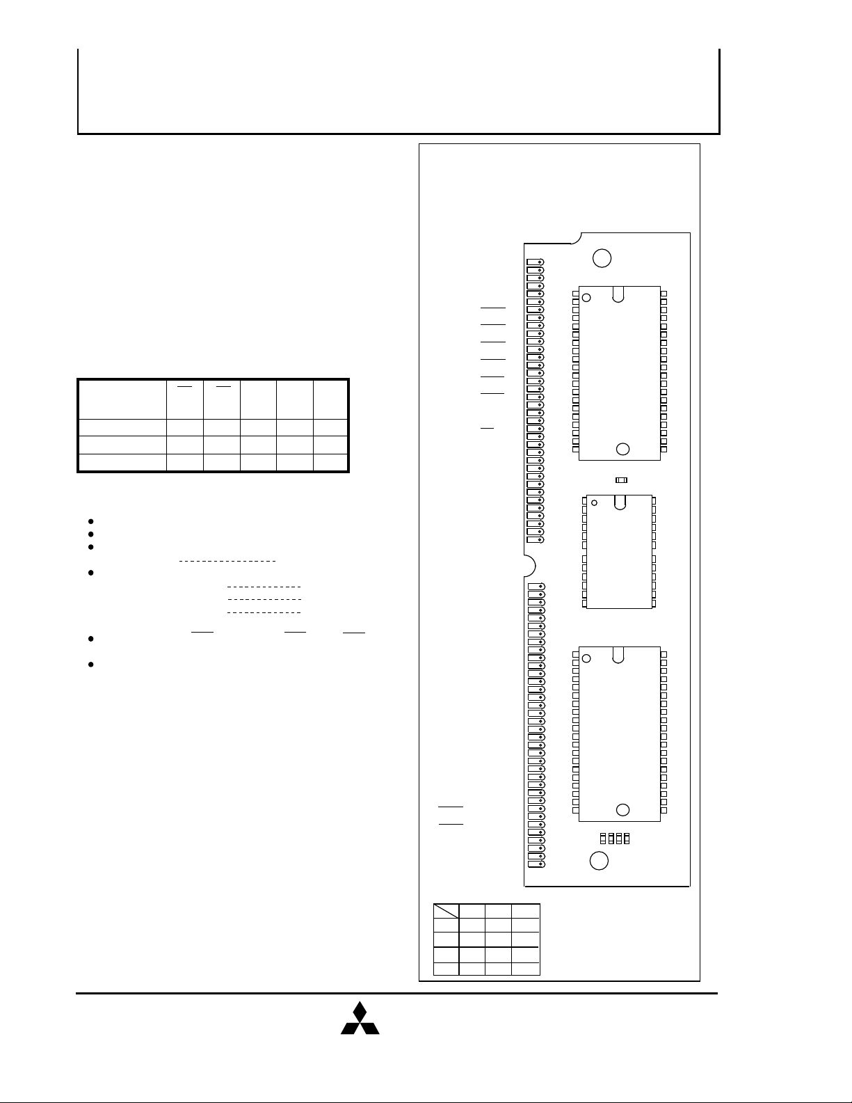
PIN CONFIGURATION (TOP VIEW)
DESCRIPTION
The MH2M365CXJ/CNXJ is 2097152-word x 36-bits dynamic
RAM. This consists of four industry standard 1M x 16 dynamic
RAMs in SOJ and two industry 1M x 4 dyanmic RAMs in SOJ.
The mounting of SOJ on a single in-line package provides any
application where high densities and large quantities of memory
are required. This is a socket-type memory module,suitable for
easy interchange or addition of modules.
FEATURES
Type name
MH2M365CXJ/CNXJ-5
MH2M365CXJ/CNXJ-6
MH2M365CXJ/CNXJ-7
access
time
(max.ns)
Address
time
(max.ns)
access
time
(max.ns)
506013152530 90
70 20 35 130
access
Cycle
time
(min.ns)
110
Power
dissipa-
tion
(typ.mW)
2137
1767
1537
RAS
CAS
72pin single in-line package
Single 5.0V ± 10% supply
Low stand-by power dissipation
33mW (Max) CMOS lnput level
Low operating power dissipation
MH2M365CXJ/CNXJ- 5 2.69W (Max)
MH2M365CXJ/CNXJ- 6 2.22W (Max)
MH2M365CXJ/CNXJ- 7 1.92W (Max)
Hyper-page mode , RAS-only refresh , CAS before RAS
refresh, Hidden refresh capabilities
All inputs and output directly TTL compatible
1024 refresh cycles every 16.4ms (A0 ~ A9)
APPLICATION
Main memory unit for computers, Microcomputer memory,
Refresh memory for CRT
1.Vss
2.DQ0
3.DQ16
4.DQ1
5.DQ17
6.DQ2
7.DQ18
8.DQ3
11.NC
10.Vcc
11.NC
12.A0
13.A1
14.A2
15.A3
16.A4
17.A5
18.A6
19.NC
20.DQ4
21.DQ20
22.DQ5
23.DQ21
24.DQ6
25.DQ22
26.DQ7
27.DQ23
28.A7
29.NC
30.Vcc
31.A8
32.A9
33.RAS3
34.RAS2
35.MP2
36.MP0
37.MP1
38.MP3
39.Vss
40.CAS0
41.CAS2
42.CAS3
43.CAS1
44.RAS0
45.RAS1
46.NC
47.W
48.NC
49.DQ8
50.DQ24
51.DQ9
52.DQ25
53.DQ10
54.DQ26
55.DQ11
56.DQ27
57.DQ12
58.DQ28
59.Vcc
60.DQ29
61.DQ13
62.DQ30
63.DQ14
64.DQ31
65.DQ15
66.NC
67.PD1
68.PD2
69.PD3
70.PD4
71.NC
72.Vss
[Double side]
1
2
3
4
5
6
7
8
9
10
11
12
13
14
15
16
17
18
19
20
21
22
23
24
25
26
27
28
29
30
31
32
33
34
35
36
37
38
39
40
41
42
43
44
45
46
47
48
49
50
51
52
53
54
55
56
57
58
59
60
61
62
63
64
65
66
67
68
69
70
71
72
MIT-DS-0083-1.2
PD1
PD2
PD3
PD4
MITSUBISHI
ELECTRIC
( / 15 )
1
- 5 - 6
NC NC
NCNC
Vss
NC
Vss
NC
- 7
NC
NC
Vss
NC
Outline 72N9J-C
NC: NO CONNECTION
21/Feb./1997
Page 2
MH2M365CXJ/CNXJ-5,-6,-7
HYPER PAGE MODE 75497472-BIT ( 2097152-WORD BY 36-BIT ) DYNAMIC RAM
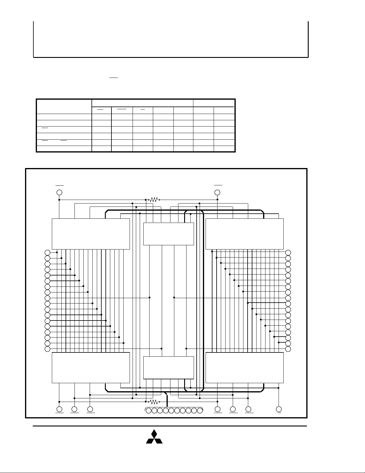
FUNCTION
in addition to normal read, write, a number of other
functions, e.g., hyper page mode, RAS only refresh,
Table 1 Input conditions for each mode
Operation
Read ACT ACT NAC
Early write
RAS-only refresh
Hidden refresh
CAS before RAS refresh
Standby
Note : ACT : active, NAC : nonactive, DNC : don' t care, VLD : valid, IVD : Invalid,APD : applied, OPN : open
RAS
ACT ACT ACT
ACT
ACT
ACT ACT DNC
NAC
CAS
NAC
ACT
DNC
W
DNC
NAC
DNC
BLOCK DIAGRAM
The input conditions for each are shown in Table 1.
Inputs
Row
address
Column
APD APD
APD APD
APD
APD
DNC DNC
DNC
address
DNC
DNC
DNC
Input/Output
Input
VLD OPN
DNC
DNC
DNC OPN
Output
VLDOPN
OPN
VLDOPN
OPN
MITSUBISHI LSIs
DQ0
DQ1
DQ2
DQ3
DQ4
DQ5
DQ6
DQ7
MP0
DQ8
DQ9
DQ10
DQ11
DQ12
DQ13
DQ14
DQ15
MP1
RAS1
45 33
LCAS UCAS LCAS UCAS
M5M418165CJ
LDATA UDATA LDATA UDATA
2
4
6
8
20
22
24
26
36
49
51
53
55
57
61
63
65
37
LDATA UDATA LDATA UDATA
M5M418165CJ
LCAS UCAS LCAS UCAS
0 1 2 3
M5M44505CJ
0 1 2 3
0 1 2 3
M5M44505CJ
0 1 2 3
RAS3
M5M418165CJ
M5M418165CJ
DQ16
3
5
DQ17
DQ18
7
9
DQ19
DQ20
21
23
DQ21
DQ22
25
27
DQ23
MP2
35
DQ24
50
DQ25
52
DQ26
54
DQ27
56
DQ28
58
DQ29
60
DQ30
62
64
DQ31
MP3
38
44 34 41 4240 43
RAS0 CAS0 CAS1 RAS2 CAS2 CAS3
MIT-DS-0083-1.2
12A013A114A215A316A417A518A628A731A832
MITSUBISHI
ELECTRIC
( / 15 )
2
47
A9
W
21/Feb./1997
Page 3
HYPER PAGE MODE 75497472-BIT ( 2097152-WORD BY 36-BIT ) DYNAMIC RAM
ABSOLUTE MAXIMUM RATINGS
Symbol
Vcc
V I
V0
I 0
Pd
Topr
Tstg
Supply voltage
Input voltage
Output voltage
Output current
Power dissipation
Operating temperature
Storage temperature
Parameter Conditions Ratings Unit
MITSUBISHI LSIs
MH2M365CXJ/CNXJ-5,-6,-7
With respect to Vss
Ta=25 C
-1 ~ 7
-1 ~ 7
-1 ~ 7
50
6000
0 ~ 70
-40 ~ 125
V
V
V
mA
mW
C
C
RECOMMENDED OPERATING CONDITIONS
Symbol
Vcc
Vss
VIH
VIL
Note 1 : All voltage values are with respect to Vss
Supply voltage
Supply voltage
High-level input voltage, all inputs
Low-level input voltage, all inputs
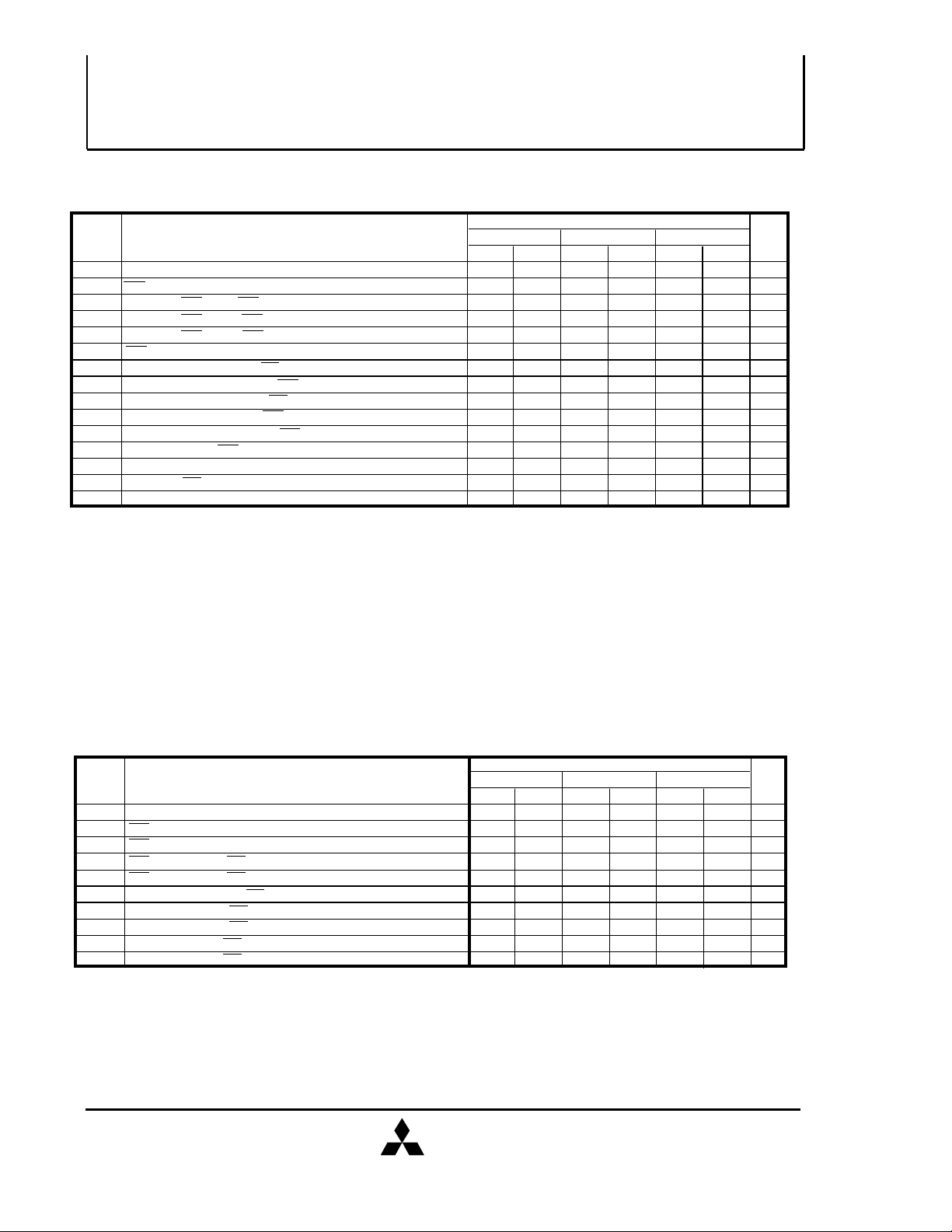
ELECTRICAL CHARACTERISTICS
Symbol
VOH
VOL
IOZ
I I
ICC1 (AV)
ICC2
ICC3 (AV)
ICC4(AV)
ICC6(AV)
Note 2: Current flowing into an IC is positive, out is negative.
3: Icc1 (AV), Icc3 (AV) and Icc4 (AV) are dependent on cycle rate. Maximum current is measured at the fastest cycle rate.
4: Icc1 (AV) and Icc4 (AV) are dependent on output loading. Specified values are obtained with the output open.
5: Column Address can be changed once or less while RAS=VIL and CAS=VIH .
High-level output voltage
Low-level output voltage
Off-state output current
Input current
Average supply current
from Vcc operating
Supply current from Vcc , stand-by
Average supply current
from Vcc refreshing
Average supply current
from Vcc
Hyper-Page-Mode
Average supply current
from Vcc
CAS before RAS refresh
mode
Parameter
Parameter
(Note 3,4,5)
(Note 3,5)
(Note 3,4,5)
(Note 3)
(Ta=0 ~ 70°C, Vcc=5.0V ± 10%, Vss=0V, unless otherwise noted) (Note 2)
MH2M365C -5
MH2M365C -6
MH2M365C -7
(Note 6)
MH2M365C -5
MH2M365C -6
MH2M365C -7
MH2M365C -5
MH2M365C -6
MH2M365C -7
MH2M365C -5
MH2M365C -6
MH2M365C -7
(Ta=0 ~ 70 °C, unless otherwise noted) (Note 1)
Limits
Min Nom Max
5.5
5.0
4.5
0
0
0
2.4
-1
IOH=-5.0mA
IOL=4.2mA
Q floating 0V ≤ VOUT ≤ 5.5V
0V ≤ VIN ≤ 6 V, Other inputs pins=0V
RAS, CAS cycling
tRC=tWC=min.
output open
RAS= CAS =VIH, output open
RAS= CAS ≥ Vcc - 0.2 V
RAS cycling, CAS= VIH
tRC=min.
output open
RAS=VIL, CAS cycling
tPC=min.
output open
CAS before RAS refresh cycling
tRC=min.
output open
6.0
0.8
Test conditions
Unit
V
V
V
V
Limits
Min Max
Typ
2.4
0
-20
-60
Vcc
0.4
20
491
406
351
12
491
406
351
461
366
311
471
391
341
Unit
V
V
µA
60
µA
mA
mA
6
mA
mA
mA
MIT-DS-0083-1.2
MITSUBISHI
ELECTRIC
( / 15 )
3
21/Feb./1997
Page 4
MITSUBISHI LSIs
MH2M365CXJ/CNXJ-5,-6,-7
HYPER PAGE MODE 75497472-BIT ( 2097152-WORD BY 36-BIT ) DYNAMIC RAM
CAPACITANCE
Symbol Parameter
CI (W)
CI (RAS)
CI (CAS)
CI / O
(Ta=0 ~ 70 °C, Vcc=5.0V ± 10%, Vss=0V, unless otherwise noted)
Input capacitance,address inputsCI (A)
Input capacitance, write control input
Input capacitance, RAS input
Input capacitance, CAS input
Input/Output capacitance, data ports
SWITCHING CHARACTERISTICS
Symbol
tCAC
tRAC
tAA
tCPA
tOHC
tOHR
tCLZ
tWEZ
tOFF
tREZ
Access time from CAS
Access time from RAS
Column address access time
Access time from CAS precharge
Output hold time from CAS 5
Output hold time from RAS
Output low impedance time from CAS low (Note 7) 5
Output disable time after WE high
Output disable time after CAS high
Output disable time after RAS high
Parameter
Test conditions
VI=Vss
f=1MHZ
Vi=25mVrms
(Ta=0 ~ 70 °C, Vcc = 5V ± 10%, Vss=0V, unless otherwise noted , see notes 6,14,15)
MH2M365C -5
Min Max
(Note 7,8)
(Note 7,9)
(Note 7,10)
(Note 7,11)
(Note 13)
(Note 12)
(Note 12,13)
(Note 12,13)
13
50
25
30
5
5
13
13
13
Limits
Min Max
Typ
45
57
36
43
29
Limits
MH2M365C -6 MH2M365C -7
Min Max
5
55 ns
Min Max
15
60
30
35
5
15
15
15
Unit
pF
pF
pF
pF
pF
Unit
ns
20
ns
70
ns
35
ns
40
ns5
ns
ns
20
ns
20
ns
20
Note 6: An initial pause of 500µs is required after power-up followed by a minimum of eight initialization cycles (any combination of cycles
containing a RAS clock such as RAS-Only refresh).
Note the RAS may be cycled during the initial pause . And any 8 RAS or RAS/CAS cycles are required after prolonged periods
(greater than 16.4 ms) of RAS inactivity before proper device operation is achieved.
7: Measured with a load circuit equivalent to VOH=2.4V(IOH=-5mA) / VOL=0.4V(IOL=-4.2mA) load 100pF.
The reference levels for measuring of output signal are 2.0V(VOH) and 0.8V(VOL).
8: Assumes that tRCD ≥ tRCD(max) and tASC ≥ tASC(max) and tCP ≥t CP(max).
9: Assumes that tRCD ≤ tRCD(max) and tRAD ≤ tRAD(max). If tRCD or tRAD is greater than the maximum recommended value shown in this table,
tRAC will increase by amount that tRCD exceeds the value shown.
10: Assumes that tRAD ≥ tRAD(max) and tASC ≤ tASC(max).
11: Assumes that tCP ≤ tCP(max) and tASC ≥ tASC(max).
12: tWEZ(max) ,tOFF(max) and tREZ(max)defines the time at which the output achieves the high impedance state ( IOUT ≤ I ± 10 µA I)
and is not reference to VOH(min) or VOL(max).
13: Output is disabled after both RAS and CAS go to high.
MIT-DS-0083-1.2
MITSUBISHI
21/Feb./1997
ELECTRIC
( / 15 )
4
Page 5
MH2M365CXJ/CNXJ-5,-6,-7
HYPER PAGE MODE 75497472-BIT ( 2097152-WORD BY 36-BIT ) DYNAMIC RAM
TIMING REQUIREMENTS (For Read, Write, Refresh, and Hyper-Page Mode Cycles)
(Ta=0 ~ 70°C, Vcc = 5V ± 10%, Vss=0V, unless otherwise noted See notes 14,15)
MITSUBISHI LSIs
40
20
5
0
10
15
0
0
10
10
00
1513
1513
1
Limits
16.4
45
30
13
50
Min Max
16.4
50
50
20
5
0
10
35
15
0
0
10
10
0
20
20
50
1
Unit
13
Symbol
tREF
tRP
tRCD
tCRP
tRPC
tCPN
tRAD
tASR
tASC
tRAH
tCAH
tDZC
Refresh cycle time
RAS high pulse width
Delay time, RAS low to CAS low
Delay time, CAS high to RAS low
Delay time, RAS high to CAS low
CAS high pulse width
Column address delay time from RAS low
Row address setup time before RAS low
Column address setup time before CAS low
Row address hold time after RAS low
Column address hold time after CAS low
Delay time, data to CAS low
tRDD
tCDD
tT
Note 14: The timing requirements are assumed tT =3ns.
15: VIH(min) and VIL(max) are reference levels for measuring timing of input signals.
16: tRCD(max) is specified as a reference point only. If tRCD is less than tRCD(max), access time is tRAC. If tRCD is greater than tRCD(max), access
time is controlled exclusively by tCAC or tAA.
17: tRAD(max) is specified as a reference point only. If tRAD ≤ tRAD(max) and tASC ≤ tASC(max), access time is controlled exclusively by tAA.
18: tASC(max) is specified as a reference point only. If tRCD ≥ tRCD(max) and tASC ≥ tASC(max), access time is controlled exclusively by tCAC.
19: tDZC must be satisfied.
20: Either tRDD or tCDD or tODD must be satisfied.
21: tT is measured between VIH(min) and VIL(max).
Delay time, CAS high to data
Transition time
Parameter
(Note16)
(Note17)
(Note18)
(Note19)
(Note20)Delay time, RAS high to data
(Note20)
(Note21)
MH2M365C -5 MH2M365C -6 MH2M365C -7
Min Max Min Max
16.4
30
18
5
8
13
8
8
37
0
25
0
10
0
50
1
ms
ns
ns
ns
ns
ns
ns
ns
ns
ns
ns
ns
ns
ns
ns
Read and Refresh Cycles
Symbol
Read cycle time
tRC
RAS low pulse width
tRAS
CAS low pulse width
tCAS
CAS hold time after RAS low
tCSH
RAS hold time after CAS low
tRSH
Read Setup time before CAS low
tRCS
Read hold time after CAS high (Note 22)
tRCH
Read hold time after RAS high
tRRH
Column address to RAS hold time
tRAL
Column address to CAS hold time
tCAL
Note 22: Either tRCH or tRRH must be satisfied for a read cycle.
Parameter
(Note 22)
MIT-DS-0083-1.2
MH2M365C -5 MH2M365C -6 MH2M365C -7
Min Max Min Max
90
50
8
40
13
0
0
10
25
13 18
MITSUBISHI
ELECTRIC
( / 15 )
5
10000
10000
110
60
10
48
10
30
Limits
15
0
0
10000
10000
Min Max
130
10000
70
10000
13
55
20
0
0
10
35
23
21/Feb./1997
Unit
ns
ns
ns
ns
ns
ns
ns
ns
ns
ns
Page 6

HYPER PAGE MODE 75497472-BIT ( 2097152-WORD BY 36-BIT ) DYNAMIC RAM
Write Cycle (Early Write)
MITSUBISHI LSIs
MH2M365CXJ/CNXJ-5,-6,-7
110
60
10
15
0
Limits
48
0
10
10
10000
10000
Min Max
130
10000
70
10000
13
55
20
0
13
13
0
13
Symbol
tWC
tRAS
tCAS
tCSH
tRSH
tWCS
tWCH
tWP
tDS
tDH
Parameter
Write cycle time
RAS low pulse width
CAS low pulse width
CAS hold time after RAS low
RAS hold time after CAS low
Write setup time before CAS low
Write hold time after CAS low
Write pulse width
Data setup time before CAS low or W low
Data hold time after CAS low or W low
MH2M365C -5 MH2M365C -6 MH2M365C -7
Min Max Min Max
90
10000
50
10000
8
40
13
0
8
8
0
8 10
Hyper page Mode Cycle (Read, Early Write, Hi-Z control by W) (Note 25)
25
77
10
35
7
Limits
55
100000
16
7
7
30
5
92
100000
13
40
16
Symbol
tHPC
tDOH
tRAS
tCP
tCPRH
tCHOL
tWPE
Note 23: All previously specified timing requirements and switching characteristics are applicable to their respective Hyper page mode cycle.
24: tRAS(min) is specified as two cycles of CAS input are performed.
25: tCP(max) is specified as a reference point only.
Hyper page mode read/write cycle time
Output hold time from CAS low
RAS low pulse width for read write cycle
CAS high pulse width
RAS hold time after CAS precharge
Hold time to maintain the data Hi-Z until CAS access
W Pulse Width (Hi-Z control)
Parameter
(Note24)
(Note25)
MH2M365C -5 MH2M365C -6 MH2M365C -7
Min Max Min MaxnsMin Max
20
65
100000
8
13
30
7
7 7
Unit
ns
ns
ns
ns
ns
ns
ns
ns
ns
ns
Unit
ns
ns
ns
ns
ns
ns
CAS before RAS Refresh Cycle (Note 26)
Symbol
CAS setup time before RAS low
tCSR
CAS hold time after RAS low
Note 26: Eight or more CAS before RAS cycles instead of eight RAS cycles are necessary for proper operation of CAS before RAS refresh
mode.
Parameter
MIT-DS-0083-1.2
MH2M365C -5 MH2M365C -6 MH2M365C -7
Min Max
5
10
MITSUBISHI
Limits
Min Max Min Max
5
10
5
15
Unit
ns
nstCHR
21/Feb./1997
ELECTRIC
( / 15 )
6
Page 7

HYPER PAGE MODE 75497472-BIT ( 2097152-WORD BY 36-BIT ) DYNAMIC RAM
Timing Diagrams (Note 27)
Read Cycle
MITSUBISHI LSIs
MH2M365CXJ/CNXJ-5,-6,-7
tRC
RAS
CAS
A0~A9
W
DQ(INPUTS)
DQ(OUTPUTS)
VIH
VIL
VIH
VIL
VIH
VIL
VIH
VIL
VIH
VIL
VOH
VOL
tCRP
tASR tRAH
ROW
ADDRESS
tRAD
tRCD
tDZC
tASC tCAH
tRCS
tRAC
COLUMN
ADDRESS
tCLZ
tRAS
tCAC
tAA
tCSH
tRAL
tCAL
tCAS
Hi-Z
tRSH
tRDD
tREZ
tOHR
DATA VALID
tRP
tCRP
tASR
ROW
ADDRESS
tRRH
tRCH
tCDD
tWEZ
tOFF
tOHC
Hi-ZHi-Z
MIT-DS-0083-1.2
Note 27
Indicates the don't care input.
VIH(min) ≤ VIN ≤ VIH(max) or
VIL(min) ≤ VIN ≤ VIL(max)
Indicates the invalid output.
MITSUBISHI
ELECTRIC
( / 15 )
7
21/Feb./1997
Page 8

Early Write Cycle
MITSUBISHI LSIs
MH2M365CXJ/CNXJ-5,-6,-7
HYPER PAGE MODE 75497472-BIT ( 2097152-WORD BY 36-BIT ) DYNAMIC RAM
tWC
RAS
CAS
A0~A9
W
DQ(INPUTS)
VIH
VIL
VIH
VIL
VIH
VIL
VIH
VIL
VIH
VIL
tCRP
tASR
tRAH
ROW
ADDRESS
tRCD
tASC
tDS
tWCS
tRAS
tCAH
COLUMN
ADDRESS
DATA VALID
tWCH
tDH
tCSH
tRSH
tCAS
tRP
tCRP
tASR
ROW
ADDRESS
DQ(OUTPUTS)
VOH
VOL
MIT-DS-0083-1.2
Hi-Z
MITSUBISHI
ELECTRIC
( / 15 )
8
21/Feb./1997
Page 9

HYPER PAGE MODE 75497472-BIT ( 2097152-WORD BY 36-BIT ) DYNAMIC RAM
Hyper Page Mode Read Cycle
MITSUBISHI LSIs
MH2M365CXJ/CNXJ-5,-6,-7
RAS
CAS
A0~A9
W
DQ(INPUTS)
DQ(OUTPUTS)
VIH
VIL
VIH
VIL
VIH
VIL
VIH
VIL
VIH
VIL
VOH
VOL
tCRP
tASR
tRAH
ROW
ADDRESS
Hi-Z
tRAD
tRCD
tASC
tRCS
tDZC
tRAC
tRAS
tCSH
tCAS
tCAH
COLUMN-1
tCAL tCAL tCAL
tCAC
tAA
tCLZ
DATA
VALID-1
tHPC
tCP
tCAS
tCAHtASC tCAHtASC
COLUMN-2 COLUMN-3
Hi-Z
tCAC
tAA
tDOH
tCPA
tCP tCAS
tCPRH
tCAC
tAA
tDOH
DATA
VALID-2
tCPA
tRP
tRSH
tASR
ROW
ADDRESS
tRRH
tRCH
tWEZ
tRDD
tCDD
tREZ
tOHR
tOFF
tOHC
DATA
VALID-3
MIT-DS-0083-1.2
MITSUBISHI
ELECTRIC
9
( / 15 )
21/Feb./1997
Page 10

HYPER PAGE MODE 75497472-BIT ( 2097152-WORD BY 36-BIT ) DYNAMIC RAM
Hyper Page Mode Early Write Cycle
MITSUBISHI LSIs
MH2M365CXJ/CNXJ-5,-6,-7
RAS
CAS
A0~A9
W
DQ(INPUTS)
VIH
VIL
VIH
VIL
VIH
VIL
VIH
VIL
VIH
VIL
tCRP
tASR
tRAH
ROW
ADDRESS
tRAS
tCSH
tRCD
tASC
tWCS
tDS tDH tDS tDH tDS tDH
tCAS
tCAH
COLUMN-1
tWCH tWCS tWCH tWCS tWCH
DATA
VALID-1
tHPC
tCP
tASC
tCAS
tCAL tCAL
tCAH
COLUMN-2 COLUMN-3
DATA
VALID-2
tRSH
tCP tCAS
tASC
tCAH
DATA
VALID-3
tRP
tCRP
tASR
ROW
ADDRESS
DQ(OUTPUTS)
VOH
VOL
MIT-DS-0083-1.2
Hi-Z
MITSUBISHI
ELECTRIC
10
( / 15 )
21/Feb./1997
Page 11

MH2M365CXJ/CNXJ-5,-6,-7
HYPER PAGE MODE 75497472-BIT ( 2097152-WORD BY 36-BIT ) DYNAMIC RAM
Hyper Page Mode Read Cycle ( Hi-Z control by W )
MITSUBISHI LSIs
RAS
CAS
A0~A9
W
DQ(INPUTS)
DQ(OUTPUTS)
VIH
VIL
VIH
VIL
VIH
VIL
VIH
VIL
VIH
VIL
VOH
VOL
tCRP
tASR
tRAH
ROW
ADDRESS
Hi-Z
tRAD
tCSH tHPC
tRCD
tASC
tRCS
tDZC
tRAC
tCAS
tCAH
COLUMN-1
tCAC
tAA
tCLZ
DATA
VALID-1
tRAS
tCP
tCAS
tCAHtASC tCAHtASC
COLUMN-2 COLUMN-3
tRCH
tCAC
tAA
tDOH
tCPA
tCP tCAS
tWPE
Hi-Z
tWEZ
DATA
VALID-2
tCPA
tAA
Hi-Z
tRSH
tCPRH
tRAL
tRCS
tCAC
tCLZ
tRP
tCRP
tASR
ROW
ADDRESS
tRRH
tRCH
tRDD
tCDD
tREZ
tOHR
tOFF
tOHC
DATA
VALID-3
MIT-DS-0083-1.2
MITSUBISHI
ELECTRIC
( / 15 )
11
21/Feb./1997
Page 12

HYPER PAGE MODE 75497472-BIT ( 2097152-WORD BY 36-BIT ) DYNAMIC RAM
RAS-only Refresh Cycle
RAS
VIH
VIL
MITSUBISHI LSIs
MH2M365CXJ/CNXJ-5,-6,-7
tRC
tRAS
tRP
CAS
A0~A9
W
DQ(INPUT)
DQ(OUTPUT)
VIH
VIL
VIH
VIL
VIH
VIL
VIH
VIL
VOH
VOL
tCRP
tASR tRAH
ADDRESS
ROW
Hi-Z
tRPC
tCRP
tASR
ROW
ADDRESS
MIT-DS-0083-1.2
MITSUBISHI
ELECTRIC
( / 15 )
12
21/Feb./1997
Page 13

HYPER PAGE MODE 75497472-BIT ( 2097152-WORD BY 36-BIT ) DYNAMIC RAM
CAS before RAS Refresh Cycle
MITSUBISHI LSIs
MH2M365CXJ/CNXJ-5,-6,-7
RAS
CAS
A0~A9
W
DQ(INPOUT)
DQ(OUTPUT)
VIH
VIL
VIH
VIL
VIH
VIL
VIH
VIL
VIH
VIL
VOH
VOL
tRPC
tRRH
tRCH
tRP
tCPN
tREZ
tOHR
tOFF
tOHC
tCSR
tCHR
tRAS
tRC
tRC
tRAS
tCSRtRPC
tCHR
Hi-Z
tRPC
tRP
tCRP
tASR
ROW
ADDRESS
COLUMN
ADDRESS
tRCS
MIT-DS-0083-1.2
MITSUBISHI
ELECTRIC
13
( / 15 )
21/Feb./1997
Page 14

HYPER PAGE MODE 75497472-BIT ( 2097152-WORD BY 36-BIT ) DYNAMIC RAM
Hidden Refresh Cycle (Read) (Note 28)
MITSUBISHI LSIs
MH2M365CXJ/CNXJ-5,-6,-7
RAS
CAS
A0~A9
W
DQ(INOUT)
DQ(OUTPUT)
VIH
VIL
VIH
VIL
VIH
VIL
VIH
VIL
VIH
VIL
VOH
VOL
tCRP
tASR
tRAH
ROW
ADDRESS
tRCD
tRAD
tASC
tRCS
tDZC
Hi-Z
tRAC
tRC
tRAS
tCAH
COLUMN
ADDRESS
tRAL
tCAC
tAA
tCLZ
tRSH
tRP
tCHR
Hi-Z
DATA VALID
tRAS
tRC
tRP
tASR
ROW
ADDRESS
tRRH
tRCH
tCDD
tRDD
tREZ
tOHR
tOFF
tOHC
Hi-Z
Note 28: Early write cycle is applicable instead of read cycle.
Timing requirements and output state are the same as that of each cycle shown above.
MIT-DS-0083-1.2
MITSUBISHI
ELECTRIC
14
( / 15 )
21/Feb./1997
Page 15

HYPER PAGE MODE 75497472-BIT ( 2097152-WORD BY 36-BIT ) DYNAMIC RAM
72pin DRAM Module Outline
20.2
MITSUBISHI LSIs
MH2M365CXJ/CNXJ-5,-6,-7
107.95
8.6MAX
101.193.38
10.16
R1.57
2.03
1 72
6.35
6.35 35x1.27=44.45 35x1.27=44.456.35
R1.57
1.27
5.96MIN.
2-ø3.18
5.96MIN.
1.27
MIT-DS-0083-1.2
MITSUBISHI
ELECTRIC
15
( / 15 )
21/Feb./1997
 Loading...