

Page 1
9,663,676,416
-BIT (134,217,728-WORD BY 72-BIT) Double Data Rate Synchronous DRAM Module
Preliminary Spec.
APPLICATION
Main memory unit for PC, PC server, Server, WS.
Type name
133MHz
MH28D72KLG-10
MH28D72KLG-75
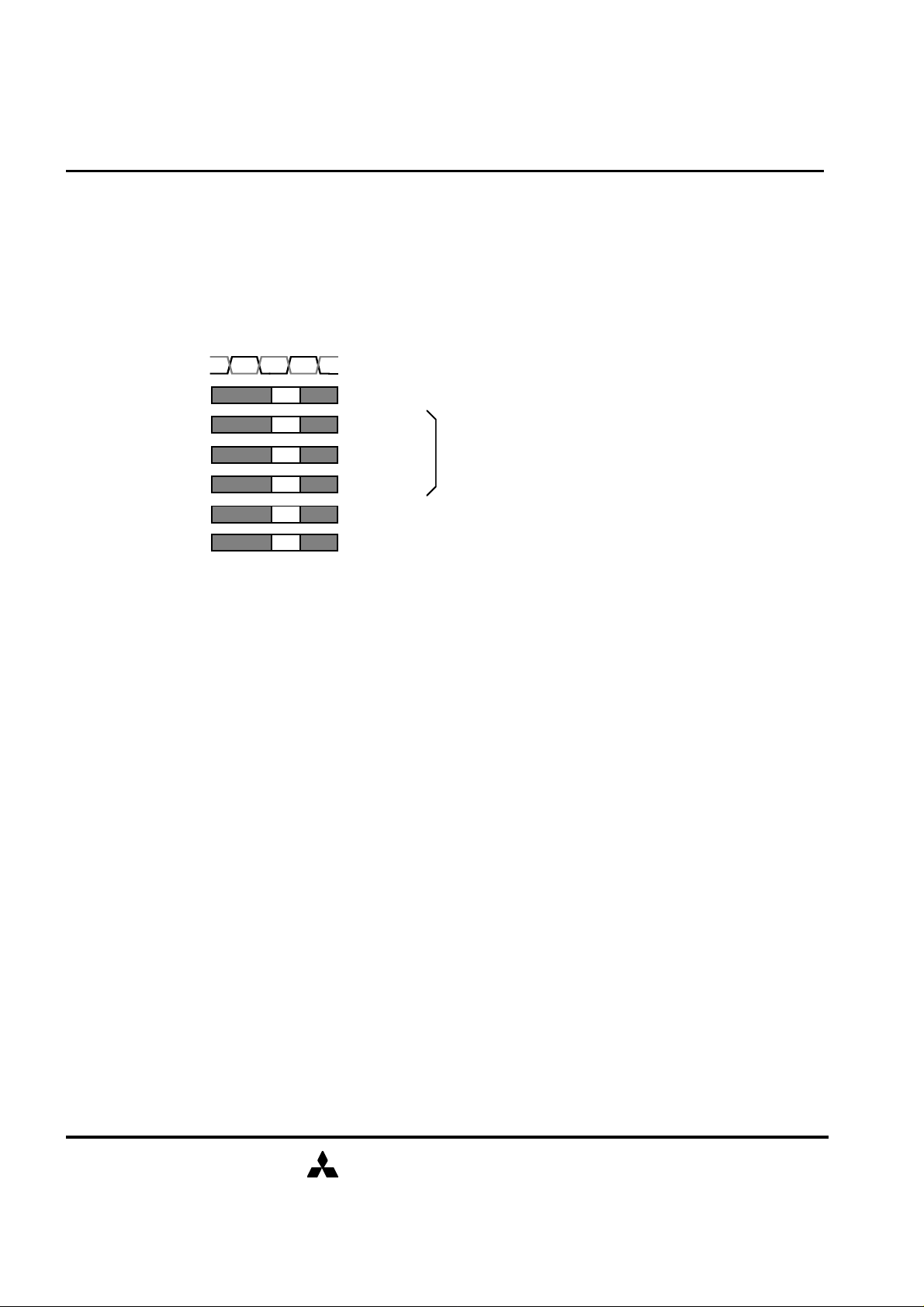
- Commands entered on each positive CLK edge
100MHz
Data Rate(DDR) Synchronous DRAM mounted module.
main
[component level]
+ 0.75ns
+ 0.8ns
Some contents are subject to change without notice.
DESCRIPTION
The MH28D72KLG is 134217728 - word x 72-bit Double
This consists of 36 industry standard 64M x 4 DDR
Synchronous DRAMs in TSOP with SSTL_2 interface which
achieves very high speed data rate up to 133MHz.
This socket-type memory module is suitable for
memory in computer systems and easy to interchange or
add modules.
FEATURES
MITSUBISHI LSIs
MH28D72KLG-75,-10
93pin
1pin
Max.
Frequency
- Utilizes industry standard 64M X 4 DDR Synchronous DRAMs
in TSOP package , industry standard Registered Buffer in
TSSOP package , and industry standard PLL in TSSOP package.
- Vdd=Vddq=2.5v±0.2V
CLK
Access Time
- Double data rate architecture; two data transfers per
clock cycle
- Bidirectional, data strobe (DQS) is transmitted/received
with data
- Differential clock inputs (CLK and /CLK)
- data referenced to both edges of DQS
- /CAS latency- 2.0/2.5 (programmable)
- Burst length- 2/4/8 (programmable)
- Auto precharge / All bank precharge controlled by A10
- 8192 refresh cycles /64ms
- Auto refresh and Self refresh
- Row address A0-12 / Column address A0-9,11
- SSTL_2 Interface
- Module 2bank Configration
- Burst Type - sequential/interleave(programmable)
144pin
145pin
184pin
52pin
53pin
92pin
MIT-DS-0412-0.1
MITSUBISHI ELECTRIC
21.Mar.2001
1
Page 2
9,663,676,416
-BIT (134,217,728-WORD BY 72-BIT) Double Data Rate Synchronous DRAM Module
Preliminary Spec.
Some contents are subject to change without notice.
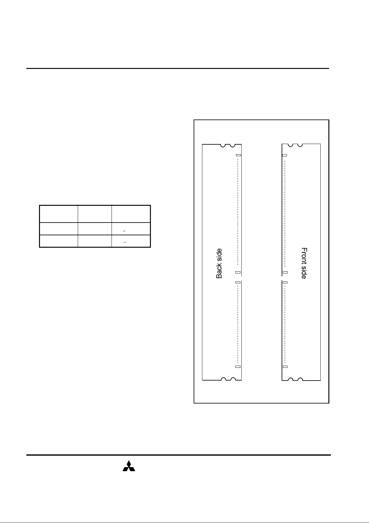
PIN CONFIGURATION
PIN
NO.
PIN
NAME
1
VREF
2
DQ0
3
VSS
4
DQ1
5
DQS0
6
DQ2
7
VDD
DQ3
NC
RESET
VSS
DQ8
DQ9
DQS1
15
VDDQ
16
17 58
18
19
20
21
22
23 DQ16 64
24 DQ17 65
25 DQS2 66
26 VSS 67
27
28
29
30
31 DQ19 72
32
33
34
35
36
37 A4 78
38
39
40
41
42
NC
NC
VSS
DQ10
DQ11
CKE0
VDDQ
A9
DQ18
A7
VDDQ
A5
DQ24
VSS
DQ25
DQS3
VDD
DQ26
DQ27
A2
VSS
PIN
NO.
43
44
45
46
47
48
49
50
51
52
53
54
55
56
57
59
60
61
62
63
68
69
70
71
73
74
75
76
77
79
80
81
82
83
KEY
PIN
NAME
A1
CB0
CB1
VDD
DQS8
A0
CB2
VSS
CB3
BA1
DQ32
VDDQ
DQ33
DQS4
DQ34
VSS
BA0
DQ35
DQ40
VDDQ
/WE
DQ41
/CAS
VSS
DQS5
DQ42
DQ43
VDD
NC
DQ48
DQ49
VSS
NC
NC
VDDQ
DQS6
DQ50
DQ51
VSS
VDDID
DQ56
PIN
NO.
84
85
86
87
88
89
90
91
92
93
94
95
96
97
98
99
100
101
102
103
104
105
106
107
108
109
110
111
112
113
114
115
116
117
118
119
120
121
122
123
124
125
PIN
NAME
DQ57
VDD
DQS7
DQ58
DQ59
VSS
NC
SDA
SCL
VSS
DQ4
DQ5
VDDQ
DQS9
DQ6
DQ7
VSS
NC
NC
NC
VDDQ
DQ12
DQ13
DQS10
VDD
DQ14
DQ15
CKE1
VDDQ
NC
DQ20
A12
VSS
DQ21
A11
DQS11
VDD
DQ22
A8
DQ23
VSS
A6
PIN
NO.
126
127
128
129
130
131
132
1338
1349
13510
13611
13712
13813
13914
140
141
142
143
144
145
146
147
148
149
150
151
152
153
154
155
156
157
158
159
160
161
162
163
164
165
166
MITSUBISHI LSIs
MH28D72KLG-75,-10
PIN
NAME
DQ28
DQ29
VDDQ
DQS12
A3
DQ30
VSS
DQ31
CB4
CB5
VDDQ
CK0
/CK0
VSS
DQS17
A10
CB6
VDDQ
CB7
KEY
VSS
DQ36
DQ37
VDD
DQS13
DQ38
DQ39
VSS
DQ44
/RAS
DQ45
VDDQ
/S0
/S1
DQS14
VSS
DQ46
DQ47
NC
VDDQ
DQ52
DQ53
PIN
NO.
167
168
169
170
171
172
173
174
175
176
177
178
179
180
181
182
183
184
PIN
NAME
NC
VDD
DQS15
DQ54
DQ55
VDDQ
NC
DQ60
DQ61
VSS
DQS16
DQ62
DQ63
VDDQ
SA0
SA1
SA2
VDDSPD
NC: No Connect
MIT-DS-0412-0.1
MITSUBISHI ELECTRIC
21.Mar.2001
2
Page 3
9,663,676,416
-BIT (134,217,728-WORD BY 72-BIT) Double Data Rate Synchronous DRAM Module
Preliminary Spec.
CK0
/CK0
Registered Buffer
SA0
SA1
SA2
SERIAL PD
SCL
SDAA0A1A2WP
VDD
D0 to D35
VREF
VSS
D0 to D35
D0 to D35
VDDID
VDDQ
D0 to D35
VDDID: OPEN -> VDD = VDDQ
DQ1
DQ2
DQ3
DM
DQS/SDM/SDQS
DQ10
DQ11
DM
DQS/SDM
/S
DQS
DQ19
DM
DQS/SDM/SDQS
DQ24
DQ27
DM
DQS/SDM/SDQS
DQ32
DQ33
DM
DQS/SDM/SDQS
DQ40
DQ41
DQ42
DM
DQS/SDM/SDQS
DQ48
DQ49
DQ50
DQ51
DM
DQS/SDM/SDQS
DQ57
DQ58
DQ59
DM
DQS/SDM/SDQS
CB2
CB3
DM
DQS
/SDM/S
DQS
DQ5
DQ6
DQ7
DM
DQS/SDM/SDQS
DQ14
DQ15
DM
DQS/SDM
/S
DQS
DQ23
DM
DQS/SDM/SDQS
DQ28
DQ31
DM
DQS/SDM/SDQS
DQ36
DQ37
DM
DQS/SDM/SDQS
DQ44
DQ45
DQ46
DM
DQS/SDM/SDQS
DQ52
DQ53
DQ54
DQ55
DM
DQS/SDM/SDQS
DQ61
DQ62
DQ63
DM
DQS/SDM/SDQS
CB6
CB7
DM
DQS
/SDM/S
DQS
D0D1D2D3D4D5D6D7D8
D18
D19
D20
D21
D22
D23
D024
D025
D026D9D10
D11
D12
D13
D14
D15
D16
D17
D27
D28
D29
D30
D31
D32
D33
D34
D35
/S0
BA0-BA1
A0-A12
/RAS
/CAS
CKE0
/WE
/RS0 -> SDRAMs D0-D17
RBA0-RBA1
-> SDRAMs D0-D35
RA0-RA12
-> SDRAMs D0-D35
/RRAS -> SDRAMs D0-D35
/RCAS -> SDRAMs D0-D35
/RCKE0 -> SDRAMs D0-D17
/RWE -> SDRAMs D0-D35
/PCK
PCK
/RESET
/S1
/RS1 -> SDRAMs D18-D35
CKE1
/RCKE1 -> SDRAMs D18-D35
VDDSPD
Serial PD
Some contents are subject to change without notice.
Block Diagram
VSS
/RS1
/RS0
DQS0
DQ0
MITSUBISHI LSIs
MH28D72KLG-75,-10
DQS9
DQ4
DQS1
DQS2
DQS3
DQS4
DQS5
DQS6
DQS7
DQ8
DQ9
DQ16
DQ17
DQ18
DQ25
DQ26
DQ34
DQ35
DQ43
DQ56
DQS10
DQS11
DQS12
DQS13
DQS14
DQS15
DQS16
DQ12
DQ13
DQ20
DQ21
DQ22
DQ29
DQ30
DQ38
DQ39
DQ47
DQ60
DQS8
CB0
CB1
PLL
DQS17
CB4
CB5
PCK0 -> SDRAMs D0-D35,
Registered Buffer
/PCK0 -> SDRAMs D0-D35,
MIT-DS-0412-0.1
MITSUBISHI ELECTRIC
VSS -> VDD = VDDQ
21.Mar.2001
3
Page 4
9,663,676,416
-BIT (134,217,728-WORD BY 72-BIT) Double Data Rate Synchronous DRAM Module
Preliminary Spec.
PIN FUNCTION
Data Input/Output: Data bus
SYMBOL
DESCRIPTION
Some contents are subject to change without notice.
TYPE
Clock: CK0 and /CK0 are differential clock inputs. All address and
CK0,/CK0 Input
CKE0, CKE1
Input
control input signals are sampled on the crossing of the positive edge
of CK0 and negative edge of /CK0. Output (read) data is referenced to
the crossings of CK0 and /CK0 (both directions of crossing).
Clock Enable: CKE0,1 controls SDRAM internal clock. When CKE0 is low, the
internal clock for the following cycle is ceased. CKE0 is also used to select
auto / self refresh. After self refresh mode is started, CKE0 becomes
asynchronous input. Self refresh is maintained as long as CKE0 is low.
MITSUBISHI LSIs
MH28D72KLG-75,-10
/S0, /S1
Input
Physical Bank Select: When /S0,1 is high, any command means No Operation.
/RAS, /CAS, /WE Input Combination of /RAS, /CAS, /WE defines basic commands.
A0-12 specify the Row / Column Address in conjunction with BA0,1. The Row
Address is specified by A0-12. The Column Address is specified by A0-9,11.
A0-12 Input
BA0,1 Input
DQ 0-64
CB 0-7
DQS0-17
Input / Output
Input / Output
A10 is also used to indicate precharge option. When A10 is high at a read / write
command, an auto precharge is performed. When A10 is high at a precharge
command, all banks are precharged.
Bank Address: BA0,1 specifies one of four banks in SDRAM to which a command is applied. BA0,1
must be set with ACT, PRE, READ, WRITE commands.
Data Strobe: Output with read data, input with write data. Edge-aligned
with read data, centered in write data. Used to capture write data.
Vdd, VddQ Power Supply Power Supply. Vdd and VddQ are connected on the module.
VddQ, VssQ Power Supply
Vddspd
Power Supply Power Supply for SPD
Vref Input
RESET
Input
Power Supply. Vss and VssQ are connected on the module.
SSTL_2 reference voltage.
This signal is asynchronous and is driven low to the register in order to
guarantee the register outputs are low.
SDA
SCL
SA0-2
VDDID
Input / Output
Input
Input
This bidirectional pin is used to transfer data into or out of the SPD EEPROM.
A resistor must be connected from the SDA bus line to VDD to act as a pullup.
This signal is used to clock data into and out of the SPD EEPROM. A resistor
may be connected from the SCL bus time to VDD to act as a pullup.
These signals are tied at the system planar to either VSS or VDD to configure
the serial SPD EEPROM address range.
VDD identification flag
MIT-DS-0412-0.1
MITSUBISHI ELECTRIC
21.Mar.2001
4
Page 5
9,663,676,416
-BIT (134,217,728-WORD BY 72-BIT) Double Data Rate Synchronous DRAM Module
Preliminary Spec.
BASIC FUNCTIONS
burst read (auto-precharge,
READA
)
WRITE command starts burst write to the active bank indicated by BA. Total data length to be
the burst write (auto-precharge,
WRITEA
).
PRE command deactivates the active bank indicated by BA. This command also terminates
(precharge all,
PREA
).
generated internally. After this command, the banks are precharged automatically.
Some contents are subject to change without notice.
MITSUBISHI LSIs
MH28D72KLG-75,-10
The MH28D72KLG provides basic functions, bank (row) activate, burst read / write, bank (row)
precharge, and auto / self refresh. Each command is defined by control signals of /RAS, /CAS
and /WE at CLK rising edge. In addition to 3 signals, /CS ,CKE and A10 are used as chip
select, refresh option, and precharge option, respectively. To know the detailed definition of
commands, please see the command truth table.
/CK0
CK0
/S0
Chip Select : L=select, H=deselect
/RAS
/CAS
/WE
CKE0
A10
Command
Command
Command
Refresh Option @refresh command
Precharge Option @precharge or read/write command
define basic commands
Activate (ACT) [/RAS =L, /CAS =/WE =H]
ACT command activates a row in an idle bank indicated by BA.
Read (READ) [/RAS =H, /CAS =L, /WE =H]
READ command starts burst read from the active bank indicated by BA. First output data
appears after /CAS latency. When A10 =H at this command, the bank is deactivated after the
Write (WRITE) [/RAS =H, /CAS =/WE =L]
written is set by burst length. When A10 =H at this command, the bank is deactivated after
Precharge (PRE) [/RAS =L, /CAS =H, /WE =L]
burst read /write operation. When A10 =H at this command, all banks are deactivated
Auto-Refresh (REFA) [/RAS =/CAS =L, /WE =CKE0 =H]
REFA command starts auto-refresh cycle. Refresh address including bank address are
MIT-DS-0412-0.1
21.Mar.2001
MITSUBISHI ELECTRIC
5
Page 6
9,663,676,416
-BIT (134,217,728-WORD BY 72-BIT) Double Data Rate Synchronous DRAM Module
Preliminary Spec.
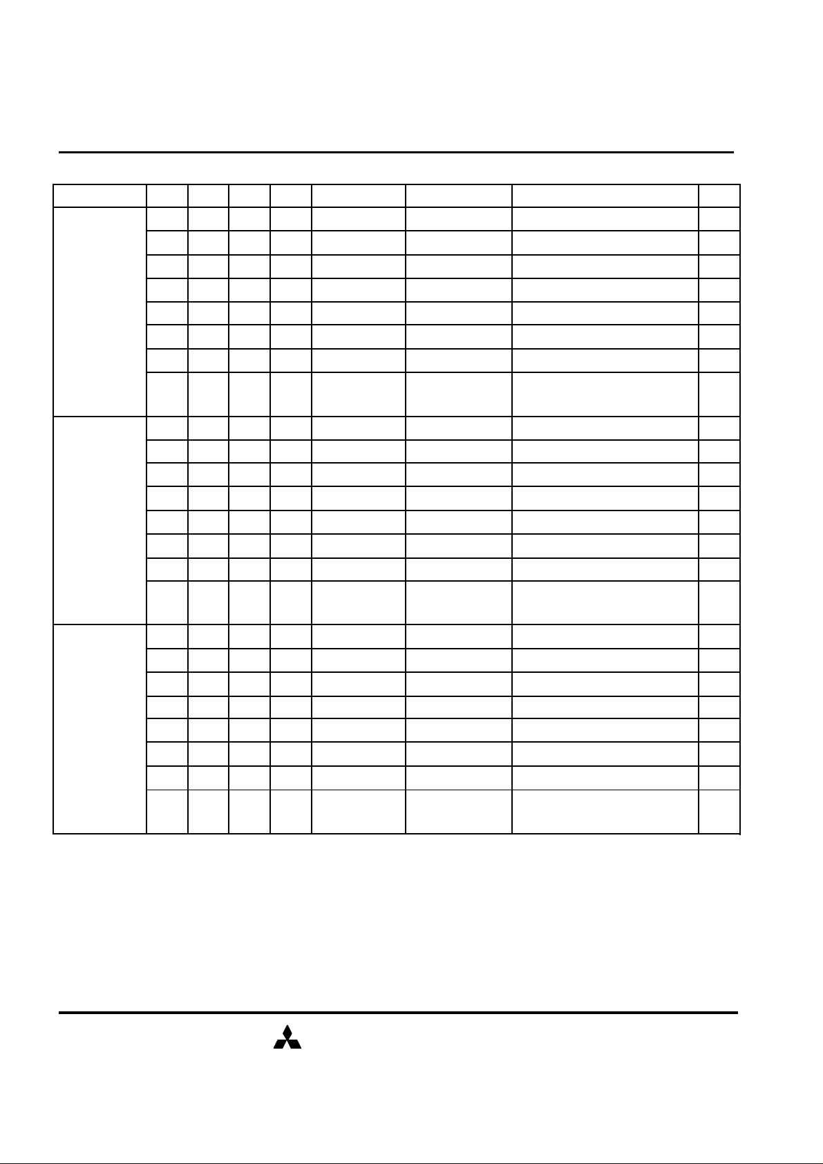
COMMAND TRUTH TABLE
Some contents are subject to change without notice.
MITSUBISHI LSIs
MH28D72KLG-75,-10
COMMAND MNEMONIC
Deselect DESEL H X H X X X X X X
No Operation NOP H X L H H H X X X
Row Address Entry &
Bank Activate
Single Bank Precharge PRE H X L L H L V L X
Precharge All Banks PREA H X L L H L H X
Column Address Entry
& Write
Column Address Entry
& Write with
Auto-Precharge
Column Address Entry
& Read
Column Address Entry
& Read with
Auto-Precharge
Auto-Refresh
Self-Refresh Entry REFS H L L L L H X X X
Self-Refresh Exit REFSX
Burst Terminate TERM H X L H H L X X X
Mode Register Set MRS H X L L L L L L V
ACT H X L L H H V V V
WRITE H X L H L L V L V
WRITEA H X L H L L V H V
READ H X L H L H V L V
READA H X L H L H V H V
REFA H H L L L H X X X
CKE
CKE
n-1
L H H X X X X X X
L H L H H H X X X
n
/S /RAS /CAS /WE BA0,1
A10
/AP
X
A0-9,
11-12
note
1
2
H=High Level, L=Low Level, V=Valid, X=Don't Care, n=CLK cycle number
NOTE:
1. Applies only to read bursts with autoprecharge disabled; this command is undefined (and should
not be used) for read bursts with autoprecharge enabled, and for write bursts.
2. BA0-BA1 select either the Base or the Extended Mode Register (BA0 = 0, BA1 = 0 selects Mode
Register; BA0 = 1, BA1 = 0 selects Extended Mode Register; other combinations of BA0-BA1 are
reserved; A0-A11 provide the op-code to be written to the selected Mode Register.
MIT-DS-0412-0.1
MITSUBISHI ELECTRIC
21.Mar.2001
6
Page 7
9,663,676,416
-BIT (134,217,728-WORD BY 72-BIT) Double Data Rate Synchronous DRAM Module
Preliminary Spec.
Notes
Some contents are subject to change without notice.
FUNCTION TRUTH TABLE
Current State
IDLE H X X X X DESEL NOP
/S
/RAS /CAS /WE Address Command Action
L H H H X NOP NOP
L H H L BA TERM ILLEGAL
MITSUBISHI LSIs
MH28D72KLG-75,-10
2
L H L X BA, CA, A10 READ / WRITE ILLEGAL
L L H H BA, RA ACT Bank Active, Latch RA
L L H L BA, A10 PRE / PREA NOP
L L L H X REFA Auto-Refresh
L L L L
ROW ACTIVE H X X X X DESEL NOP
L H H H X NOP NOP
L H H L BA TERM NOP
L H L H BA, CA, A10 READ / READA
L H L L BA, CA, A10
L L H H BA, RA ACT Bank Active / ILLEGAL
L L H L BA, A10 PRE / PREA Precharge / Precharge All
L L L H X REFA ILLEGAL
L L L L
READ
(Auto-
Precharge
Disabled)
H X X X X DESEL NOP (Continue Burst to END)
L H H H X NOP NOP (Continue Burst to END)
L H H L BA TERM Terminate Burst
L H L H BA, CA, A10 READ / READA
L H L L BA, CA, A10
L L H H BA, RA ACT Bank Active / ILLEGAL
Op-Code,
Mode-Add
Op-Code,
Mode-Add
MRS Mode Register Set
Begin Read, Latch CA,
Determine Auto-Precharge
WRITE /
WRITEA
MRS ILLEGAL
WRITE
WRITEA
Begin Write, Latch CA,
Determine Auto-Precharge
Terminate Burst, Latch CA,
Begin New Read, Determine
Auto-Precharge
ILLEGAL
2
4
5
5
2
3
2
L L H L BA, A10 PRE / PREA Terminate Burst, Precharge
L L L H X REFA ILLEGAL
L L L L
MIT-DS-0412-0.1
Op-Code,
Mode-Add
MITSUBISHI ELECTRIC
MRS ILLEGAL
21.Mar.2001
7
Page 8
9,663,676,416
-BIT (134,217,728-WORD BY 72-BIT) Double Data Rate Synchronous DRAM Module
Preliminary Spec.
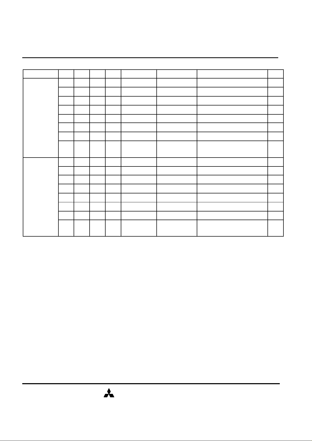
FUNCTION TRUTH TABLE (continued)
Notes
Some contents are subject to change without notice.
MITSUBISHI LSIs
MH28D72KLG-75,-10
Current State
WRITE
(Auto-
Precharge
Disabled)
READ with
AUTO
PRECHARGE
/S
/RAS /CAS /WE Address Command Action
H X X X X DESEL NOP (Continue Burst to END)
L H H H X NOP NOP (Continue Burst to END)
L H H L BA TERM ILLEGAL
Terminate Burst, Latch CA,
L H L H BA, CA, A10 READ / READA
L H L L BA, CA, A10
L L H H BA, RA ACT Bank Active / ILLEGAL
L L H L BA, A10 PRE / PREA Terminate Burst, Precharge
L L L H X REFA ILLEGAL
L L L L
H X X X X DESEL NOP (Continue Burst to END)
L H H H X NOP NOP (Continue Burst to END)
L H H L BA TERM ILLEGAL
L H L H BA, CA, A10 READ / READA ILLEGAL
Op-Code,
Mode-Add
WRITE /
WRITEA
MRS ILLEGAL
Begin Read, Determine AutoPrecharge
Terminate Burst, Latch CA,
Begin Write, Determine AutoPrecharge
3
3
2
WRITE with
AUTO
PRECHARGE
L H L L BA, CA, A10
L L H H BA, RA ACT Bank Active / ILLEGAL
L L H L BA, A10 PRE / PREA PRECHARGE/ILLEGAL
L L L H X REFA ILLEGAL
L L L L
H X X X X DESEL NOP (Continue Burst to END)
L H H H X NOP NOP (Continue Burst to END)
L H H L BA TERM ILLEGAL
L H L H BA, CA, A10 READ / READA ILLEGAL
L H L L BA, CA, A10
L L H H BA, RA ACT Bank Active / ILLEGAL
L L H L BA, A10 PRE / PREA PRECHARGE/ILLEGAL
L L L H X REFA ILLEGAL
L L L L
Op-Code,
Mode-Add
Op-Code,
Mode-Add
WRITE /
WRITEA
MRS ILLEGAL
WRITE /
WRITEA
MRS ILLEGAL
ILLEGAL
ILLEGAL
2
2
2
2
MIT-DS-0412-0.1
MITSUBISHI ELECTRIC
21.Mar.2001
8
Page 9
9,663,676,416
-BIT (134,217,728-WORD BY 72-BIT) Double Data Rate Synchronous DRAM Module
Preliminary Spec.
FUNCTION TRUTH TABLE (continued)
Notes
Some contents are subject to change without notice.
MITSUBISHI LSIs
MH28D72KLG-75,-10
Current State
PRE -
CHARGING
ROW
ACTIVATING
/S
/RAS /CAS /WE Address Command Action
H X X X X DESEL NOP (Idle after tRP)
L H H H X NOP NOP (Idle after tRP)
L H H L BA TERM ILLEGAL
L H L X BA, CA, A10 READ / WRITE ILLEGAL
L L H H BA, RA ACT ILLEGAL
L L H L BA, A10 PRE / PREA NOP (Idle after tRP)
L L L H X REFA ILLEGAL
L L L L
H X X X X DESEL NOP (Row Active after tRCD)
L H H H X NOP NOP (Row Active after tRCD)
L H H L BA TERM ILLEGAL
L H L X BA, CA, A10 READ / WRITE ILLEGAL
L L H H BA, RA ACT ILLEGAL
L L H L BA, A10 PRE / PREA ILLEGAL
L L L H X REFA ILLEGAL
L L L L
Op-Code,
Mode-Add
Op-Code,
Mode-Add
MRS ILLEGAL
MRS ILLEGAL
2
2
2
4
2
2
2
2
WRITE RECOVERING
MIT-DS-0412-0.1
H X X X X DESEL NOP
L H H H X NOP NOP
L H H L BA TERM ILLEGAL
L H L X BA, CA, A10 READ / WRITE ILLEGAL
L L H H BA, RA ACT ILLEGAL
L L H L BA, A10 PRE / PREA ILLEGAL
L L L H X REFA ILLEGAL
L L L L
Op-Code,
Mode-Add
MRS ILLEGAL
MITSUBISHI ELECTRIC
2
2
2
2
21.Mar.2001
9
Page 10
9,663,676,416
-BIT (134,217,728-WORD BY 72-BIT) Double Data Rate Synchronous DRAM Module
Preliminary Spec.
FUNCTION TRUTH TABLE (continued)
Notes
Some contents are subject to change without notice.
MITSUBISHI LSIs
MH28D72KLG-75,-10
Current State
RE-
FRESHING
MODE
REGISTER
SETTING
/S
/RAS /CAS /WE Address Command Action
H X X X X DESEL NOP (Idle after tRC)
L H H H X NOP NOP (Idle after tRC)
L H H L BA TERM ILLEGAL
L H L X BA, CA, A10 READ / WRITE ILLEGAL
L L H H BA, RA ACT ILLEGAL
L L H L BA, A10 PRE / PREA ILLEGAL
L L L H X REFA ILLEGAL
L L L L
H X X X X DESEL NOP (Idle after tRSC)
L H H H X NOP NOP (Idle after tRSC)
L H H L BA TERM ILLEGAL
L H L X BA, CA, A10 READ / WRITE ILLEGAL
L L H H BA, RA ACT ILLEGAL
L L H L BA, A10 PRE / PREA ILLEGAL
L L L H X REFA ILLEGAL
L L L L
Op-Code,
Mode-Add
Op-Code,
Mode-Add
MRS ILLEGAL
MRS ILLEGAL
ABBREVIATIONS:
H=High Level, L=Low Level, X=Don't Care
BA=Bank Address, RA=Row Address, CA=Column Address, NOP=No Operation
NOTES:
1. All entries assume that CKE0 was High during the preceding clock cycle and the current clock cycle.
2. ILLEGAL to bank in specified state; function may be legal in the bank indicated by BA, depending on the state of
that bank.
3. Must satisfy bus contention, bus turn around, write recovery requirements.
4. NOP to bank precharging or in idle state. May precharge bank indicated by BA.
5. ILLEGAL if any bank is not idle.
ILLEGAL = Device operation and/or data-integrity are not guaranteed.
MIT-DS-0412-0.1
21.Mar.2001
MITSUBISHI ELECTRIC
10
Page 11
9,663,676,416
-BIT (134,217,728-WORD BY 72-BIT) Double Data Rate Synchronous DRAM Module
Preliminary Spec.
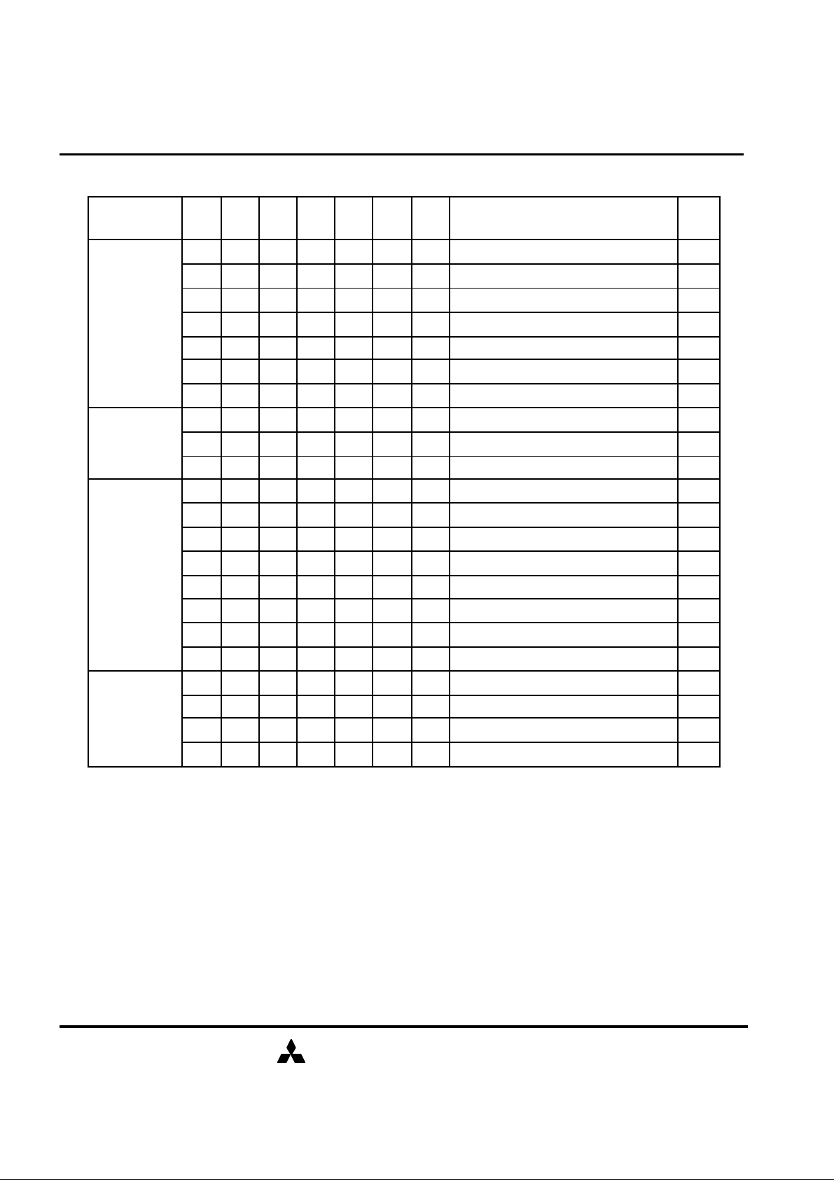
FUNCTION TRUTH TABLE for CKE
asynchronously
Notes
Some contents are subject to change without notice.
CKE
Current State
SELF-
REFRESH
POWER
DOWN
ALL BANKS
IDLE
CKE
n-1
H X X X X X X INVALID
L H H X X X X Exit Self-Refresh (Idle after tRC)
L H L H H H X Exit Self-Refresh (Idle after tRC)
L H L H H L X ILLEGAL
L H L H L X X ILLEGAL
L H L L X X X ILLEGAL
L L X X X X X NOP (Maintain Self-Refresh)
H X X X X X X INVALID
L H X X X X X Exit Power Down to Idle
L L X X X X X NOP (Maintain Self-Refresh)
H H X X X X X Refer to Function Truth Table
H L L L L H X Enter Self-Refresh
H L H X X X X Enter Power Down
H L L H H H X Enter Power Down
H L L H H L X ILLEGAL
H L L H L X X ILLEGAL
H L L L X X X ILLEGAL
L X X X X X X Refer to Current State =Power Down
/S
n
/RAS /CAS
MITSUBISHI LSIs
MH28D72KLG-75,-10
/WE Add Action
1
1
1
1
1
1
1
2
2
2
2
2
2
2
2
ANY STATE
other than
listed above
ABBREVIATIONS:
H=High Level, L=Low Level, X=Don't Care
NOTES:
1. CKE0 Low to High transition will re-enable CK0 and other inputs
. A minimum setup time must be satisfied before any command other than EXIT.
2. Power-Down and Self-Refresh can be entered only from the All Banks Idle State.
3. Must be legal command.
MIT-DS-0412-0.1
H H X X X X X Refer to Function Truth Table
H L X X X X X Begin CLK Suspend at Next Cycle
L H X X X X X Exit CLK Suspend at Next Cycle
L L X X X X X Maintain CLK Suspend
MITSUBISHI ELECTRIC
3
3
21.Mar.2001
11
Page 12
9,663,676,416
-BIT (134,217,728-WORD BY 72-BIT) Double Data Rate Synchronous DRAM Module
Preliminary Spec.
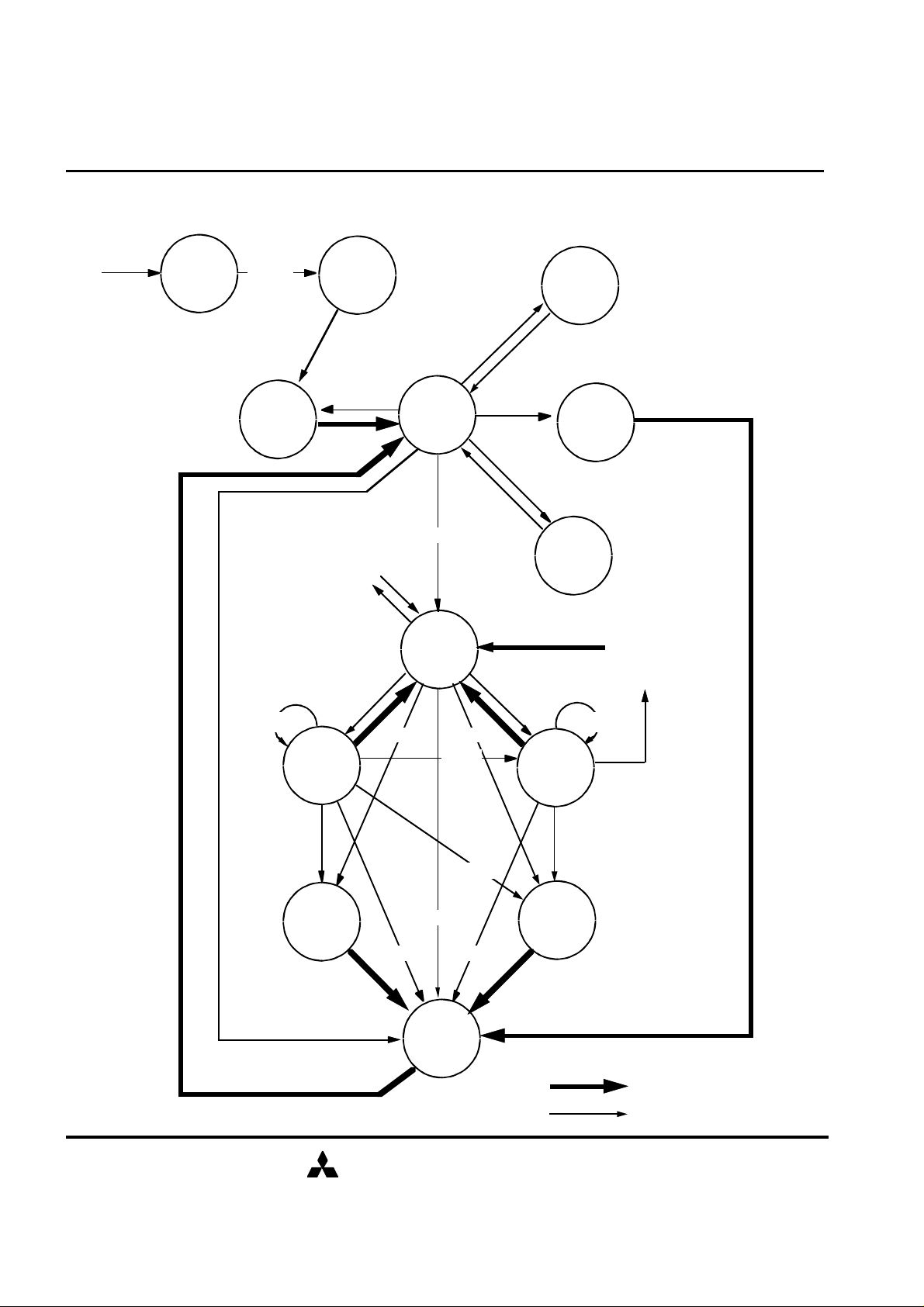
SIMPLIFIED STATE DIAGRAM
REGISTER
Some contents are subject to change without notice.
MITSUBISHI LSIs
MH28D72KLG-75,-10
POWER
APPLIED
POWER
ON
PREA
MODE
SET
PRE
CHARGE
ALL
MRS
MRS
Active
Power
Down
CKEH
CKEL
ACTIVE
IDLE
ACT
ROW
REFS
CKEH
REFSX
REFA
CKEL
SELF
REFRESH
AUTO
REFRESH
POWER
DOWN
BURST
STOP
WRITE READ
WRITE READ
WRITEA
WRITE
WRITEA READA
PRE PRE
PRE
READA
READ
READA
READ
READAWRITEA
PRE
CHARGE
TERM
Automatic Sequence
Command Sequence
MIT-DS-0412-0.1
MITSUBISHI ELECTRIC
21.Mar.2001
12
Page 13
9,663,676,416
-BIT (134,217,728-WORD BY 72-BIT) Double Data Rate Synchronous DRAM Module
Preliminary Spec.
POWER ON SEQUENCE
MODE REGISTER
Some contents are subject to change without notice.
MITSUBISHI LSIs
MH28D72KLG-75,-10
Before starting normal operation, the following power on sequence is necessary to prevent a SDRAM
from damaged or multifunctioning.
1. Apply VDD and VDDQ before or the same time as VTT & Vref
2. Maintain stable condition for 200us after stable power and CLK, apply NOP or DSEL
3. Issue precharge command for all banks of the device
4. Issue EMRS
5. Issue MRS
6. Issue 2 or more Auto Refresh commands
7. Maintain stable condition for 200 cycle
After these sequence, the SDRAM is idle state and ready for normal operation.
Burst Length, Burst Type and /CAS Latency can be programmed by
setting the mode register (MRS). The mode register stores these data until
the next MRS command, which may be issued in idle state.
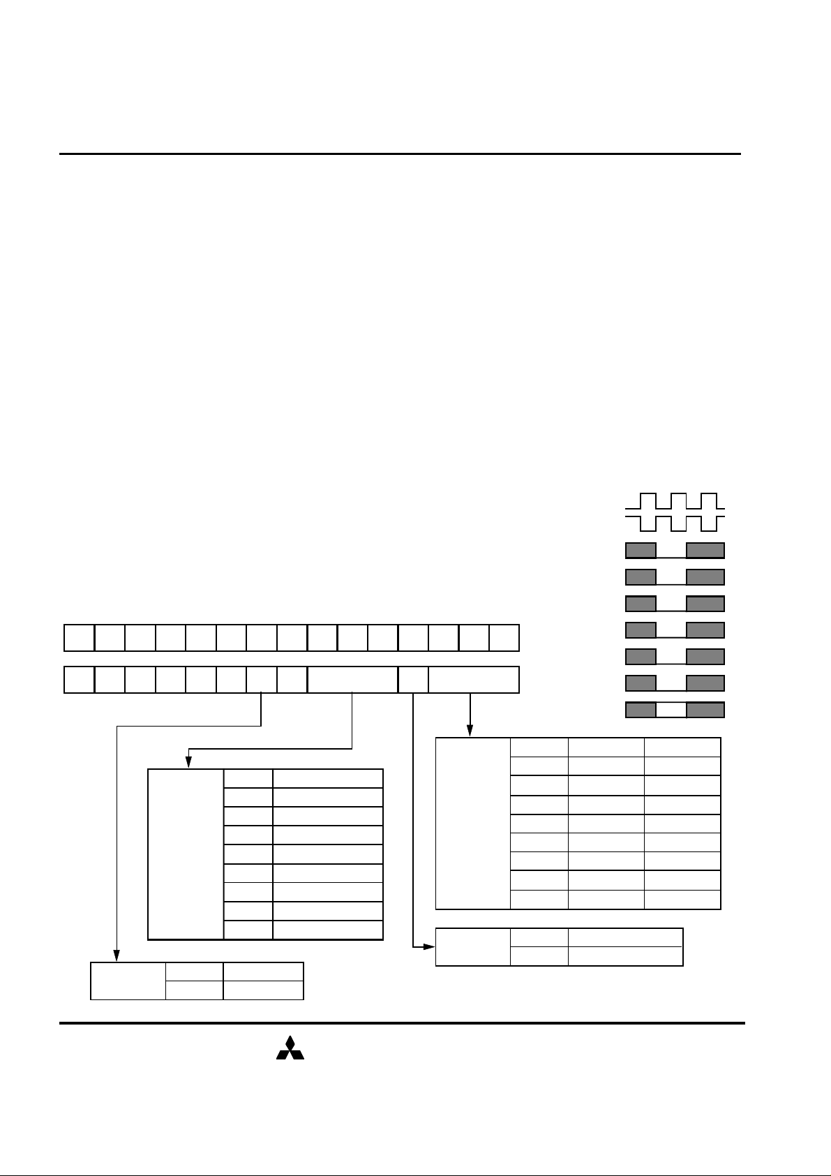
After tMRD from a MRS command, the DDR DIMM is ready for new
command.
BA1 BA0
0
DLL
Reset
A11 A10 A9 A8 A7 A6 A5 A4 A3 A2 A1 A0
A12
0 0 DR
00 0
Latency
Mode *1
(SDRAM
level)
0
1
CL
0 0 0
0 0 1
0 1 0
0 1 1
1 0 0
1 0 1
1 1 0
1 1 1
0 LTMODE BT BL
/CAS Latency
R
R
2
R
R
R
2.5
R
NO
YES
*1 In the module, 1latency should be added due to registered DIMM.
Burst
Length
Burst
Type
R: Reserved for Future Use
BL
0 0 0
0 0 1
0 1 0
0 1 1
1 0 0
1 0 1
1 1 0
1 1 1
0
1
CK0
/CK0
/S0
/RAS
/CAS
/WE
BA0
BA1
A11-A0
BT= 0 BT= 1
R
2
4
8
R
R
R
R
Sequential
Interleaved
V
R
2
4
8
R
R
R
R
MIT-DS-0412-0.1
MITSUBISHI ELECTRIC
21.Mar.2001
13
Page 14
9,663,676,416
-BIT (134,217,728-WORD BY 72-BIT) Double Data Rate Synchronous DRAM Module
Preliminary Spec.
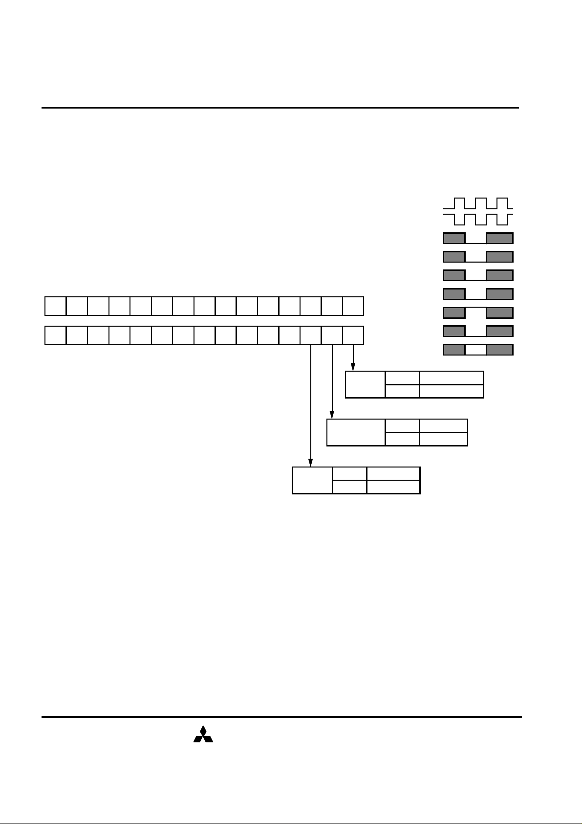
EXTENDED MODE REGISTER
Some contents are subject to change without notice.
MH28D72KLG-75,-10
DLL disable / enable mode can be programmed by setting the extended
mode register (EMRS). The extended mode register stores these data
until the next EMRS command, which may be issued in idle state.
After tMRD from a EMRS command, the DDR DIMM is ready for new
command.
A11 A10 A9 A8 A7 A6 A5 A4 A3 A2 A1 A0BA1 BA0
A12
MITSUBISHI LSIs
CK0
/CK0
/S0
/RAS
/CAS
/WE
BA0
0
0 0 0 0 DD1
0
0
QFC
DSQFC0 0 0 0
Drive
Strength
0
1
DLL
Disable
Disable
Enable
BA1
A11-A0
0
1
0
1
V
DLL enable
DLL disable
Normal
Weak
MIT-DS-0412-0.1
MITSUBISHI ELECTRIC
21.Mar.2001
14
Page 15

9,663,676,416
-BIT (134,217,728-WORD BY 72-BIT) Double Data Rate Synchronous DRAM Module
Preliminary Spec.
Write
Some contents are subject to change without notice.
( Componennt Level )
/CLK
CLK
Command
Read
MITSUBISHI LSIs
MH28D72KLG-75,-10
Address
DQS
DQ
CL= 2
BL= 4
Initial Address BL
A2 A1 A0
0 0 0
0 0 1
0 1 0
0 1 1
8
1 0 0
Y Y
Q0 Q1 Q2 Q3 D0 D1 D2 D3
/CAS
Latency
0 1 2 3 4 5 6 7 0 1 2 3 4 5 6 7
1 2 3 4 5 6 7 0 1 0 3 2 5 4 7 6
2 3 4 5 6 7 0 1 2 3 0 1 6 7 4 5
3 4 5 6 7 0 1 2 3 2 1 0 7 6 5 4
4 5 6 7 0 1 2 3 4 5 6 7 0 1 2 3
Burst
Length
Column Addressing
Sequential Interleaved
Burst
Length
1 0 1
1 1 0
1 1 1
- 0 0
- 0 1
- 1 0
- 1 1
- - 0
- - 1
MIT-DS-0412-0.1
5 6 7 0 1 2 3 4 5 4 7 6 1 0 3 2
6 7 0 1 2 3 4 5 6 7 4 5 2 3 0 1
7 0 1 2
0 1 2 3
1 2 3 0
4
2 3 0 1
3 0
0 1
2
1 0
3 4 5 6 3 2 1 0
1 2
7 6 5 4
0 1 2 3
1 0 3 2
2 3 0 1
3 2
0 1
1 0
1 0
MITSUBISHI ELECTRIC
21.Mar.2001
15
Page 16

9,663,676,416
-BIT (134,217,728-WORD BY 72-BIT) Double Data Rate Synchronous DRAM Module
Preliminary Spec.
ABSOLUTE MAXIMUM RATINGS
DC OPERATING CONDITIONS
CAPACITANCE
Conditions
Ratings
Limits
Notes
f =1MHz
Some contents are subject to change without notice.
MITSUBISHI LSIs
MH28D72KLG-75,-10
Symbol Parameter
Vdd Supply Voltage with respect to Vss -0.5 ~ 3.7 V
VddQ Supply Voltage for Output with respect to VssQ -0.5 ~ 3.7 V
VI Input Voltage with respect to Vss -0.5 ~ Vdd+0.5 V
VO Output Voltage with respect to VssQ -0.5 ~ VddQ+0.5 V
IO Output Current
Pd Power Dissipation Ta = 25°C
Topr Operating Temperature 0 ~ 70
Tstg Storage Temperature -40 ~ 100
50
20
(Ta=0 ~ 70°C , unless otherwise noted)
Symbol Parameter
Vdd/VddQ Supply Voltage 2.3 2.5 2.7 V
Vref Input Reference Voltage 1.15 1.35 V
Min. Typ. Max.
1.25
Unit
mA
W
°C
°C
Unit
5
VIH(DC) High-Level Input Voltage
VIL(DC) Low-Level Input Voltage -0.3 Vref - 0.18 V
VIN(DC) Input Voltage Level, CK0 and /CK0 -0.3 VddQ + 0.3 V
VID(DC)
VTT I/O Termination Voltage Vref - 0.04 VVref + 0.04
Input Differential Voltage, CK0 and /CK0
Vref + 0.18
0.36 VddQ + 0.6 V
VddQ+0.3 V
(Ta=0 ~ 70°C , Vdd = VddQ = 2.5 ± 0.2V, Vss = VssQ = 0V, unless otherwise noted)
Symbol
CI(A)
CI(C)
CI(K)
CI/O
Parameter
Input Capacitance, address pin
Input Capacitance, control pin
Input Capacitance, CK0 pin
Input Capacitance, I/O pin
Test Condition
Limits(max.)
17
17
8
20
Unit
pF
pF
pF
pF
7
6
Notes
11
11
11
11
MIT-DS-0412-0.1
MITSUBISHI ELECTRIC
21.Mar.2001
16
Page 17

9,663,676,416
-BIT (134,217,728-WORD BY 72-BIT) Double Data Rate Synchronous DRAM Module
Preliminary Spec.
AVERAGE SUPPLY CURRENT from Vdd
AC OPERATING CONDITIONS AND CHARACTERISTICS
-10
-75
Limits(max)
Notes
Some contents are subject to change without notice.
MITSUBISHI LSIs
MH28D72KLG-75,-10
(Ta=0 ~ 70°C , Vdd = VddQ = 2.5 ± 0.2V, Vss = VssQ = 0V, Output Open, unless otherwise noted)
Symbol
IDD0
IDD1
IDD2P
IDD2N
IDD3P
IDD3N
IDD4R
IDD4W
IDD5
IDD6
Parameter/Test Conditions
OPERATING CURRENT: One Bank; Active-Precharge;
t RC = t RC MIN; t CK = t CK MIN; DQ, DM and DQS inputs changing
twice per clock cycle; address and control inputs changing once per
clock cycle
OPERATING CURRENT: One Bank; Active-Read-Precharge;
Burst = 2; t RC = t RC MIN; CL = 2.5; t CK = t CK MIN; IOUT= 0
mA;Address and control inputs changing once per clock cycle
PRECHARGE POWER-DOWN STANDBY CURRENT: All banks idle;
power-down mode; CKE VIL (MAX); t CK = t CK MIN
IDLE STANDBY CURRENT: /CS > VIH (MIN); All banks idle;
CKE > VIH (MIN); t CK = t CK MIN; Address and other control inputs
changing once per clock cycle
ACTIVE POWER-DOWN STANDBY CURRENT: One bank active;
power-down mode; CKE VIL (MAX); t CK = t CK MIN
ACTIVE STANDBY CURRENT: /CS > VIH (MIN); CKE > VIH (MIN);
One bank; Active-Precharge; t RC = t RAS MAX; t CK = t CK MIN;
DQ,DM and DQS inputs changing twice per clock cycle; address and
other control inputs changing once per clock cycle
OPERATING CURRENT: Burst = 2; Reads; Continuous burst;One
bank active; Address and control inputs changing once per clock
cycle; CL = 2.5; t CK = t CK MIN; IOUT = 0 mA
OPERATING CURRENT: Burst = 2; Writes; Continuous burst; One
bank active; Address and control inputs changing once per clock
cycle; CL = 2.5; t CK = t CK MIN; DQ, DM and DQS inputs changing
twice per clock cycle
AUTO REFRESH CURRENT: t RC = t RFC (MIN)
SELF REFRESH CURRENT: CKE 0.2V
1469
25202819
27442909
12141289
1394
13941469
18442009
33743629
31043269
40044259
908983
mA
mA
mA
mA
mA
mA
mA
mA
mA
mA
NotesUnit
9
(Ta=0 ~ 70°C , Vdd = VddQ = 2.5 ± 0.2V, Vss = VssQ = 0V, unless otherwise noted)
Symbol Parameter/Test Conditions
VIH(AC)
VIL(AC)
VID(AC)
VIX(AC)
IOZ
Ii
High-Level Input Voltage (AC)
Low-Level Input Voltage (AC)
Input Differential Voltage, CLK and /CLK
Input Crossing Point Voltage, CLK and /CLK
Off-state Output Current /Q floating Vo=0~VDDQ
Input Current / VIN=0 ~ VddQ
0.5*VDDQ-0.2
MIT-DS-0412-0.1
MITSUBISHI ELECTRIC
Limits
Min. Max.
Vref + 0.35
0.7
0.5*VDDQ+0.2
-5
-10
Vref - 0.35VV
VDDQ + 0.6
5
10
Unit
V
7
V
8
µA
µA
21.Mar.2001
17
Page 18

9,663,676,416
-BIT (134,217,728-WORD BY 72-BIT) Double Data Rate Synchronous DRAM Module
Preliminary Spec.
Some contents are subject to change without notice.
MH28D72KLG-75,-10
AC TIMING REQUIREMENTS (Component Level)
(Ta=0 ~ 70°C , Vdd = VddQ = 2.5 ± 0.2V, Vss = VssQ = 0V, unless otherwise noted)
AC Characteristics -10-75
MITSUBISHI LSIs
Max.Min.Max.Min.Parameter
NotesUnitSymbol
DQ Output Valid data delay time from CLK//CLK nstAC
tCH CLK High level width
CLK half periodtHP
CLK cycle timetCK
tDH
tDS
tDIPW DQ and DM input pulse width (for each input)
tHZ Data-out-high impedance time from CLK//CLK
tDQSQ DQS-DQ Skew(for DQS and associated DQ signals)
tQH DQ/DQS output hold time from DQS
tDQSS Write command to first DQS latching transition
tDQSH DQS input High level width
tDQSL DQS input Low level width
tDSS DQS falling edge to CLK setup time
tDSH DQS falling edge hold time from CLK
tMRD Mode Register Set command cycle time
tWPRES Write preamble setup time
tWPST Write postamble
tWPRE Write preamble
tIS Input Setup time (address and control)
Input Setup time (DQ,DM)
Input Hold time(DQ,DM)
Data-out-low impedance time from CLK//CLKtLZ
Input Hold time (address and control)tIH
Read postambletRPST
min
(tCL,tCH)
min
(tCL,tCH)
0.60.5
0.60.5
21.75
tHP-1.0tHP-0.75
0.350.35
0.350.35
0.20.2
0.20.2
1515
00
0.250.25
1.10.9
1.10.9
+0.8-0.8+0.75-0.75
+0.8-0.8+0.75-0.75
0.55
+0.8-0.8+0.75-0.75
+0.8-0.8+0.75-0.75
+0.6+0.5
1.250.751.250.75
0.60.40.60.4
0.60.40.60.4
nsDQ Output Valid data delay time from CLK//CLKtDQSCK
tCK0.450.550.45
tCK0.550.450.550.45CLK Low level widthtCL
ns
ns158157.5CL=2.5
ns15101510CL=2
ns
ns
ns
ns
ns
ns
ns+0.6+0.5DQS-DQ Skew(for DQS and all DQ signals)tDQSA
ns
tCK
tCK
tCK
tCK
tCK
ns
ns
tCK
tCK
ns
ns
tCK
20
14
14
16
15
19
19
Read preambletRPRE
MIT-DS-0412-0.1
MITSUBISHI ELECTRIC
1.10.91.10.9
tCK
21.Mar.2001
18
Page 19

9,663,676,416
-BIT (134,217,728-WORD BY 72-BIT) Double Data Rate Synchronous DRAM Module
Preliminary Spec.
V
OUT
V
REF
30pF
VTT=V
REF
10cm
Some contents are subject to change without notice.
MH28D72KLG-75,-10
AC TIMING REQUIREMENTS(Continues)
(Ta=0 ~ 70°C , Vdd = VddQ = 2.5 ± 0.2V, Vss = VssQ = 0V, unless otherwise noted)
MITSUBISHI LSIs
-10-75AC Characteristics
Row Active time nstRAS
tRFC Auto Ref. to Active/Auto Ref. command period
tRCD
tRP
Row to Column Delay
Row Precharge time
tRRD Act to Act Delay time
tWR Write Recovery time
tWTR Internal Write to Read Command Delay
tXSNR Exit Self Ref. to non-Read command
tXSRD Exit Self Ref. to -Read command
Exit Power down to commandtXPNR
Exit Power down to -Read commandtXPRD
Average Periodic Refresh intervaltREFI
Max.Min.Max.Min.Parameter
NotesUnitSymbol
120,00050120,00045
7065
8075
2020
2020
1515
1515
nsRow Cycle time(operation)tRC
ns
ns
ns
ns
ns
ns3535Auto Precharge write recovery + precharge timetDAL
11
8075
200200
11
11
tCK
ns
tCK
tCK
tCK
us
18
177.87.8
Output Load Condition
(for component measurement)
Zo=50 ohm
MIT-DS-0412-0.1
50ohm
DQS
MITSUBISHI ELECTRIC
DQ
Output Timing
Measurement
Reference
Point
VREF
VREF
21.Mar.2001
19
Page 20

9,663,676,416
-BIT (134,217,728-WORD BY 72-BIT) Double Data Rate Synchronous DRAM Module
Preliminary Spec.
signal crossing the AC input level, and will remain in that state as long as the signal does not ring back
CLK edge. A valid transition is defined as monotonic, and meeting the input slew rate specifications of the device. When
Some contents are subject to change without notice.
MITSUBISHI LSIs
MH28D72KLG-75,-10
Notes
1. All voltages referenced to Vss.
2. Tests for AC timing, IDD, and electrical, AC and DC characteristics, may be conducted at nominal reference/supply
voltage levels, but the related specifications and device operation are guaranteed for the full voltage range specified.
3. AC timing and IDD tests may use a VIL to VIH swing of up to 1.5V in the test environment, but input timing is still
referenced to VREF (or to the crossing point for CK//CK), and parameter specifications are guaranteed for the specified
AC input levels under normal use conditions. The minimum slew rate for the input signals is 1V/ns in the range
between VIL(AC) and VIH(AC).
4. The AC and DC input level specifications are as defined in the SSTL_2 Standard (i.e. the receiver will effectively switch
as a result of the
above (below) the DC input LOW (HIGH) level.
5. VREF is expected to be equal to 0.5*VddQ of the transmitting device, and to track variations in the DC level of the
same. Peak-to-peak noise on VREF may not exceed +/-2% of the DC value.
6. VTT is not applied directly to the device. VTT is a system supply for signal termination resistors, is expected to be set
equal to VREF, and must track variations in the DC level of VREF.
7. VID is the magnitude of the difference between the input level on CLK and the input level on /CLK.
8. The value of VIX is expected to equal 0.5*VddQ of the transmitting device and must track variations in the DC level of
the same.
9. Enables on-chip refresh and address counters.
10. IDD specification are tested after the device is properly initialized.
11. This parameter is sampled. VddQ = +2.5V+/-0.2V, Vdd = +2.5V+/-0.2V, f =100MHz, Ta = 25 , VOUT(DC)=
VddQ/2, VOUT(PEAK TO PEAK) = 25mV, DM inputs are grouped with I/O pins - reflecting the fact that they are
matched in laoding (to faciliate trace matching at the board level).
12. The CLK//CLK input reference level (for signals other than CLK//CLK) is the point at which CLK and /CLK cross;
the input reference level for signals other than CLK//CLK, is VREF.
13. Inputs are not recognized as valid until VREF stabilized. Exception: during the period before VREF stabilizes, CKE=<
0.3VddQ is recognized as LOW.
14. t HZ and tLZ transitions occur in the same access time windows as valid data transitions. These parameters are not
referenced to a specific voltage level, but specify when the device output is no longer driving (HZ), or begins driving
(LZ).
15. The maximum limit for this parameter is not a device limit. The device will operate with a greater value for this
parameter, but system performance (bus turnaround) will degrade accordingly.
16. The specific requirement is that DQS be valid (HIGH, LOW, or at some point on a valid transition) on or before this
O
C
no writes were previously in progress on the bus, DQS will be transitioning from High-Z to logic LOW. If a previous
write was in progress, DQS could be HIGH, LOW, or transitioning from HIGH to LOW at this time, depending on
tDQSS.
17. A maximum of eight AUTO REFRESH commands can be posted to any given DDR SDRAM device.
18. tXPRD should be 200 tCLK in the condition of the unstable CLK operation during the power down mode.
19. For command/address and CLK & /CLK slew rate >1.0V/ns.
20. Min(tCL, tCH)refers to the smaller of the actual clock low time and the actualclock high time as provided to the
device.
MIT-DS-0412-0.1
MITSUBISHI ELECTRIC
21.Mar.2001
20
Page 21

9,663,676,416
-BIT (134,217,728-WORD BY 72-BIT) Double Data Rate Synchronous DRAM Module
Preliminary Spec.
Data
Some contents are subject to change without notice.
(Component Level)
MITSUBISHI LSIs
MH28D72KLG-75,-10
Read Operation
/CLK
CLK
Cmd &
Add.
tRPRE
DQS
DQ
Write Operation / tDQSS=max.
/CLK
CLK
DQS
tDQSS
tWPRES
tDQSCK
tDV
tDSS
tAC
tCLtCHtCK
tIS tIH
Valid
tRPST
tDQSQ
tWPST
VREF
DQ
Write Operation / tDQSS=min.
/CLK
CLK
DQS
tDQSS
tWPRES
tWPRE
DQ
MIT-DS-0412-0.1
tWPRE
tDQSL
tDS tDH
tDSH
tDQSL
tDS tDH
tDQSH
MITSUBISHI ELECTRIC
tDQSH
tWPST
21.Mar.2001
21
Page 22

9,663,676,416
-BIT (134,217,728-WORD BY 72-BIT) Double Data Rate Synchronous DRAM Module
Preliminary Spec.
tRAS
tRP
Qa0
BL/2
Qa1
Qa2
Qa3
Qa4
Qa5
Qa6
Qa7
Some contents are subject to change without notice.
MITSUBISHI LSIs
MH28D72KLG-75,-10
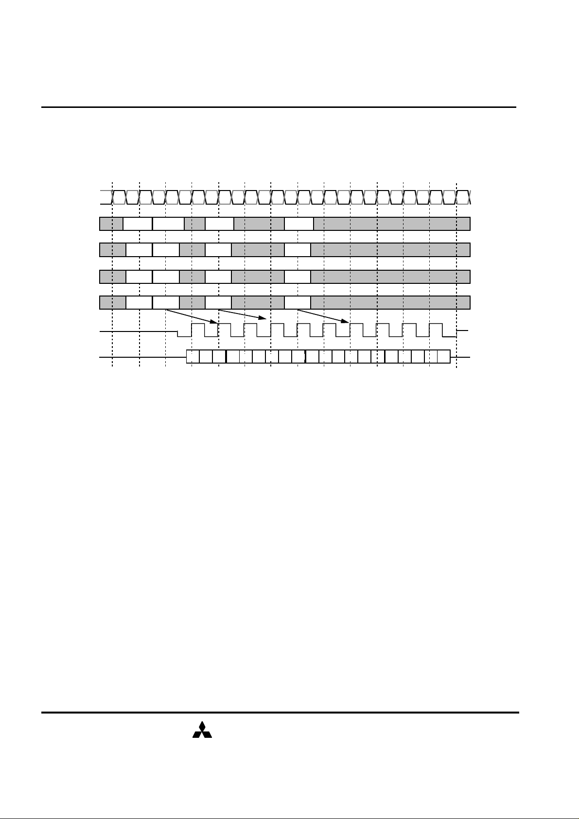
OPERATIONAL DESCRIPTION
BANK ACTIVATE
The DDR SDRAM has four independent banks. Each bank is activated by the ACT command
with the bank addresses (BA0,1). A row is indicated by the row address A12-0. The minimum
activation interval between one bank and the other bank is tRRD. Maximum 2 ACT commands
are allowed within tRC,although the number of banks which are active concurrently is not limited.
PRECHARGE
The PRE command deactivates the bank indicated by BA0,1. When multiple banks are active,
the precharge all command (PREA,PRE+A10=H) is available to deactivate them at the same
time. After tRP from the precharge, an ACT command to the same bank can be issued.
Bank Activation and Precharge All (BL=8, CL=2 (Discrete level))
Module input and output timing.
/CLK
CLK
Command
2 ACT command / tRCmin
ACT
ACT
tRRD
READ
tRCmin
PRE
ACT
A0-9,11-12
A10
BA0,1
Xa
Xa
00
tRCD
Xb
Xb
01
0
00
Y
1
Xb
Xb
01
DQS
DQ
Precharge all
A precharge command can be issued at BL/2(Discrete) from a read command without data loss.
MIT-DS-0412-0.1
MITSUBISHI ELECTRIC
21.Mar.2001
22
Page 23

9,663,676,416
-BIT (134,217,728-WORD BY 72-BIT) Double Data Rate Synchronous DRAM Module
Preliminary Spec.
Qa0
Qa1
Qa2
Qa3
Qa4
Qa5
Qa6
Qa7
Qb0
Qb1
Qb2
Qb3
Qb4
Qb5
Qb7
Some contents are subject to change without notice.
MITSUBISHI LSIs
MH28D72KLG-75,-10
READ
After tRCD from the bank activation, a READ command can be issued. 1st Output data is
available after the /CAS Latency from the READ, followed by (BL-1) consecutive data when the
Burst Length is BL. The start address is specified by A11,A9-A0, and the address sequence of burst data
is defined by the Burst Type. A READ command may be applied to any active bank, so the row
precharge time (tRP) can be hidden behind continuous output data by interleaving the
multiple banks. When A10 is high at a READ command, the auto-precharge(READA) is
performed. Any command(READ,WRITE,PRE,ACT) to the same bank is inhibited till the internal
precharge is complete. The internal precharge starts at BL/2(Discrete, In case of module, BL/2+1) after
READA. The next ACT command can be issued after (BL/2+tRP) from the previous READA.
Multi Bank Interleaving READ (BL=8, CL=2(Discrete level))
Module input and output timing.
/CLK
CLK
Command
A0-9,11-12
A10
BA0,1
DQS
DQ
ACT
Xa
Xa
00
tRCD
READ
ACT
Y
Xb
Xb
0
00
10
Module /CAS latency(Discrete CL + 1)
READ
Y
0
10
Burst Length
PRE
0
00
MIT-DS-0412-0.1
MITSUBISHI ELECTRIC
21.Mar.2001
23
Page 24

9,663,676,416
-BIT (134,217,728-WORD BY 72-BIT) Double Data Rate Synchronous DRAM Module
Preliminary Spec.
BL/2
Qa0
Qa1
Qa2
Qa3
Qa4
Qa5
Qa6
Qa7
BL/2
Qa0
Qa0
Qa1
Qa2
Qa3
Qa4
Qa5
Qa6
Qa7
Qa1
Qa2
Qa3
Qa4
Qa5
Qa6
Qa7
Some contents are subject to change without notice.
READ with Auto-Precharge (BL=8, CL=2(Discrete))
Module input and output timing.
/CLK
CLK
Command
A0-9,11-12
ACT
READ
tRCD tRP
Xa
Y
MITSUBISHI LSIs
MH28D72KLG-75,-10
BL/2 + tRP
ACT
Xb
A10
BA0,1
Xa
00
DQS
DQ
Module input and output timing.
/CLK
CLK
Module
CL=3.5
Command
Discrete
CL=2.5
DQ
ACT READ
1
00
Xb
00
Internal precharge start
(BL/2+1 in case of Module)
READ Auto-Precharge Timing (BL=8)
CL=3
DQCL=2
Internal Precharge Start Timing
(In case of module, Precharge start at BL/2+1)
MIT-DS-0412-0.1
MITSUBISHI ELECTRIC
21.Mar.2001
24
Page 25

9,663,676,416
-BIT (134,217,728-WORD BY 72-BIT) Double Data Rate Synchronous DRAM Module
Preliminary Spec.
Some contents are subject to change without notice.
MITSUBISHI LSIs
MH28D72KLG-75,-10
WRITE
After tRCD from the bank activation, a WRITE command can be issued. 1st input data is set from the
WRITE command with data strobe input, following (BL-1) data are written into RAM, when the Burst
Length is BL. The start address is specified by A11,A9-A0, and the address sequence of burst data is
defined by the Burst Type. A WRITE command may be applied to any active bank, so the row precharge
time (tRP) can be hidden behind continuous input data by interleaving the multiple banks. From the last
data to the PRE command, the write recovery time (tWRP) is required. When A10 is high at a WRITE
command, the auto-precharge(WRITEA) is performed. Any command(READ,WRITE,PRE,ACT) to the
same bank is inhibited till the internal precharge is complete. The next ACT command can be issued after
tDAL from the last input data cycle.
Module input and output timing.
/CLK
CLK
Command
A0-9,11-12
A10
BA0,1
ACT
tRCD
Xa
Xa 0
Xa
00
DQS
DQ
Module input and output timing.
/CLK
CLK
Command
A0-9,11-12
ACT
tRCD
Xa
Multi Bank Interleaving WRITE (BL=8)
WRITE
ACT
tRCD
Xb
Ya
Xb
0 0
00
10
Da0 Da1 Da2 Da3 Da4 Da5 Da6 Da7 Db0 Db1 Db2 Db3 Db4 Db5 Db6 Db7
WRITE
Yb
10
PRE
00
WRITE with Auto-Precharge (BL=8)
WRITE
tDAL
Y
PRE
0
10
ACT
Xb
A10
BA0,1
Xa
00
1
00
DQS
Da0
DQ
Da1 Da2 Da3 Da4 Da5 Da6 Da7
MIT-DS-0412-0.1
MITSUBISHI ELECTRIC
Xb
00
21.Mar.2001
25
Page 26

9,663,676,416
-BIT (134,217,728-WORD BY 72-BIT) Double Data Rate Synchronous DRAM Module
Preliminary Spec.
Q0Q1Q2Q3Q0
Q1
Yi
YjYkYl
Qak0
Qak1
Qak2
Qak3
Qak4
Qak5
Q0Q1Q2Q3Q4
Q5
Some contents are subject to change without notice.
MITSUBISHI LSIs
MH28D72KLG-75,-10
BURST INTERRUPTION
[Read Interrupted by Read]
Burst read operation can be interrupted by new read of any bank. Random column access is allowed.
READ to READ interval is minimum 1CLK.
Module input and output timing.
Read Interrupted by Read (BL=8, CL=2(Discrete))
/CLK
CLK
Command
READ READ
READ
READ
A0-9,11
A10
BA0,1
0
00
00
1000
0
01
DQS
DQ
Qai0 Qai1 Qaj0 Qaj1 Qaj2 Qaj3
Qal0 Qal1 Qal2 Qal3 Qal4 Qal5 Qal6 Qal7
[Read Interrupted by precharge]
Burst read operation can be interrupted by precharge of the same bank. READ to PRE interval is
minimum 1 CLK. A PRE command to output disable latency is equivalent to the /CAS Latency. As
a result, READ to PRE interval determines valid data length to be output. The figure below shows
examples of BL=8.
Module input and output timing.
/CLK
CLK
Command
Read Interrupted by Precharge (BL=8)
PREREAD
DQS
Module
CL=3.5
Command
DQ
READ PRE
Discrete
CL=2.5
MIT-DS-0412-0.1
DQS
DQ
Command
DQS
DQ
READ PRE
MITSUBISHI ELECTRIC
21.Mar.2001
26
Page 27

9,663,676,416
-BIT (134,217,728-WORD BY 72-BIT) Double Data Rate Synchronous DRAM Module
Preliminary Spec.
Q0Q1Q2Q3Q0
Q1DQQ0Q1Q2Q3Q4
Q5
Some contents are subject to change without notice.
MITSUBISHI LSIs
MH28D72KLG-75,-10
Module input and output timing.
/CLK
CLK
Command
DQS
Module
CL=3.0
Command
Discrete
CL=2.0
DQS
DQ
Command
DQS
DQ
Read Interrupted by Precharge (BL=8)
PREREAD
READ PRE
READ PRE
MIT-DS-0412-0.1
MITSUBISHI ELECTRIC
21.Mar.2001
27
Page 28

9,663,676,416
-BIT (134,217,728-WORD BY 72-BIT) Double Data Rate Synchronous DRAM Module
Preliminary Spec.
Q0Q1Q2Q3Q0
Q1
Q0Q1Q2Q3Q4
Q5
Q0Q1Q2Q3Q0
Q1DQQ0Q1Q2Q3Q4
Q5
Some contents are subject to change without notice.
MITSUBISHI LSIs
MH28D72KLG-75,-10
[Read Interrupted by Burst Stop]
Burst read operation can be interrupted by a burst stop command(TERM). READ to TERM
interval is minimum 1 CLK. A TERM command to output disable latency is equivalent to the /CAS
Latency. As a result, READ to TERM interval determines valid data length to be output. The figure
below shows examples of BL=8.
Module input and output timing.
/CLK
CLK
Command
DQS
Module
CL=3.5
DQ
Command
Discrete
CL=2.5
DQS
DQ
Command
DQS
DQ
Command
DQS
Read Interrupted by TERM (BL=8)
READ
READ
READ
READ
TERM
TERM
TERM
TERM
Module
CL=3.0
Discrete
CL=2.0
MIT-DS-0412-0.1
Command
DQS
DQ
Command
DQS
DQ
READ
READ
TERM
TERM
MITSUBISHI ELECTRIC
21.Mar.2001
28
Page 29

9,663,676,416
-BIT (134,217,728-WORD BY 72-BIT) Double Data Rate Synchronous DRAM Module
Preliminary Spec.
Q0Q1Q2
Q3
D0D1D2
D3
Q0Q1Q2
Q3
D0D1D2D3D4
D5
Some contents are subject to change without notice.
[Read Interrupted by Write with TERM]
MITSUBISHI LSIs
MH28D72KLG-75,-10
Module input and output timing.
/CLK
Module
CL=3.5
CLK
Command
Discrete
CL=2.5
DQS
DQ
Module
CL=3.0
Command
Discrete
CL=2.0
DQS
DQ
Read Interrupted by TERM (BL=8)
READ
READ
TERM
TERM
WRITE
WRITE
MIT-DS-0412-0.1
MITSUBISHI ELECTRIC
21.Mar.2001
29
Page 30
9,663,676,416
-BIT (134,217,728-WORD BY 72-BIT) Double Data Rate Synchronous DRAM Module
Preliminary Spec.
Yi
Yj
Yl
Dal2
Dal3
Dal5
Dal6
Dal7
Dal4
Dal0
Dak4
Dak2
Dak0
Dai0
Daj0
Daj2
Some contents are subject to change without notice.
MITSUBISHI LSIs
MH28D72KLG-75,-10
[Write interrupted by Write]
Burst write operation can be interrupted by write of any bank. Random column access is
allowed. WRITE to WRITE interval is minimum 1 CLK.
Module input and output timing.
/CLK
CLK
Write Interrupted by Write (BL=8)
Command
A0-9,11
A10
BA0,1
DQS
DQ
WRITE
0
00
WRITE
0
00
WRITE
WRITE
Yk
0
10
Dai1 Daj1 Daj3 Dak1 Dak3 Dak5 Dal1
0
00
MIT-DS-0412-0.1
MITSUBISHI ELECTRIC
21.Mar.2001
30
Page 31

9,663,676,416
-BIT (134,217,728-WORD BY 72-BIT) Double Data Rate Synchronous DRAM Module
Preliminary Spec.
The auto-refresh is performed on 4 banks concurrently. Before performing an auto refresh, all banks must
Some contents are subject to change without notice.
[Initialize and Mode Register sets]
/CLK
CLK
MITSUBISHI LSIs
MH28D72KLG-75,-10
Command
A0-9,11,12
A10
BA0,1
DQS
DQ
1
EMRSPRENOP MRS PRE AR AR MRS ACT
Code Code Xa
Code
1 0
Code Xa
0 0 0 0
tMRD tMRD tRP tRFC tRFC tMRD
1
Code
Code
Xa
[AUTO REFRESH]
Single cycle of auto-refresh is initiated with a REFA(/CS=/RAS=/CAS=L,/WE=CKE=H) command. The
refresh address is generated internally. 8192 REFA cycles within 64ms refresh 256Mbits memory cells.
be in the idle state. Auto-refresh to auto-refresh interval is minimum tRFC . Any command must not be
supplied to the device before tRFC from the REFA command.
/CLK
CLK
/CS
/RAS
/CAS
/WE
CKE
A0-12
BA0,1
MIT-DS-0412-0.1
Auto-Refresh
NOP or DESELECT
tRFC
Auto Refresh on All Banks
MITSUBISHI ELECTRIC
Auto Refresh on All Banks
21.Mar.2001
31
Page 32

9,663,676,416
-BIT (134,217,728-WORD BY 72-BIT) Double Data Rate Synchronous DRAM Module
Preliminary Spec.
is asynchronous and the only enable input, all other inputs including CLK are disabled and ignored, so that
Self-Refresh
Self Refresh Exit
Some contents are subject to change without notice.
MITSUBISHI LSIs
MH28D72KLG-75,-10
[SELF REFRESH]
Self -refresh mode is entered by issuing a REFS command (/CS=/RAS=/CAS=L,/WE=H,CKE=L). Once
the self-refresh is initiated, it is maintained as long as CKE is kept low. During the self-refresh mode, CKE
power consumption due to synchronous inputs is saved. To exit the self-refresh, supplying stable CLK
inputs, asserting DESEL or NOP command and then asserting CKE for longer than tXSNR/tXSRD.
/CLK
CLK
/CS
/RAS
/CAS
/WE
CKE
A0-12
BA0,1
tXSNR
X Y
X Y
tXSRD
Act
Read
MIT-DS-0412-0.1
21.Mar.2001
MITSUBISHI ELECTRIC
32
Page 33

9,663,676,416
-BIT (134,217,728-WORD BY 72-BIT) Double Data Rate Synchronous DRAM Module
Preliminary Spec.
Self Refresh Exit
Some contents are subject to change without notice.
MITSUBISHI LSIs
MH28D72KLG-75,-10
[Asynchronous SELF REFRESH]
Asynchronous Self -refresh mode is entered by CKE=L within 2 tCLK after issuing a REFA command
(/CS=/RAS=/CAS=L,/WE=H). Once the self-refresh is initiated, it is maintained as long as CKE is kept
low. During the self-refresh mode, CKE is asynchronous and the only enable input, all other inputs
including CLK are disabled and ignored, so that power consumption due to synchronous inputs is saved.
To exit the self-refresh, supplying stable CLK inputs, asserting DESEL or NOP command and then
asserting CKE for longer than tXSNR/tXSRD.
Asynchronous Self-Refresh
/CLK
CLK
/CS
/RAS
/CAS
/WE
CKE
A0-12
BA0,1
max 2 tCLK
tXSNR
Act
MIT-DS-0412-0.1
MITSUBISHI ELECTRIC
21.Mar.2001
33
Page 34

9,663,676,416
-BIT (134,217,728-WORD BY 72-BIT) Double Data Rate Synchronous DRAM Module
Preliminary Spec.
Some contents are subject to change without notice.
MITSUBISHI LSIs
MH28D72KLG-75,-10
[Power DOWN]
The purpose of CLK suspend is power down. CKE is synchronous input except during the self-refresh
mode. A command at cycle is ignored. From CKE=H to normal function, DLL recovery time is NOT
required in the condition of the stable CLK operation during the power down mode.
Power Down by CKE
/CLK
CLK
CKE
Standby Power
Down
Command
CKE
Command
PRE
ACT
NOP
NOP
Active Power
Down
NOP
NOP
Valid
tXPNR/
tXPRD
Valid
MIT-DS-0412-0.1
MITSUBISHI ELECTRIC
21.Mar.2001
34
Page 35

9,663,676,416
-BIT (134,217,728-WORD BY 72-BIT) Double Data Rate Synchronous DRAM Module
Preliminary Spec.
Serial Presence Detect Table I
SDRAM Cycletime at Max. Supported CAS Latency (CL).
ECC
MIimum Clock Delay, Random Column Access
Registered with PLL
VDD + 0.2V
SDRAM Access form Clock(2nd highest CAS latency)
SDRAM Access form Clock(3rd highest CAS latency)
-10
-75
-75
-10
-75
-10
-75
-10
-75
-10
Differential Clock
-75
-10
-75
-10
Some contents are subject to change without notice.
MITSUBISHI LSIs
MH28D72KLG-75,-10
Byte
Number of Serial PD Bytes Written during Production
0
1 Total # bytes of SPD memory device
2 Fundamental memory type
3 # Row Addresses on this assembly
4 # Column Addresses on this assembly
5 # Module Banks on this assembly
6 Data Width of this assembly...
7 ... Data Width continuation
8 Voltage interface standard of this assembly
9
10 SDRAM Access from Clock
11 DIMM Configuration type (Non-parity,Parity,ECC)
12 Refresh Rate/Type
13 SDRAM width,Primary DRAM
14 Error Checking SDRAM data width
15
16 Burst Lengths Supported
17
18 CAS# Latency
19 CS# Latency
20 WE Latency
21 SDRAM Module Attributes
22 SDRAM Device Attributes:General
23
SDRAM Cycle time(2nd highest CAS latency)
Function described
Cycle time for CL=2.5
tAC for CL=2.5
Number of Device Banks
Cycle time for CL=2
SPD enrty data
128 80
256 Bytes
SDRAM DDR
13
11
2BANK 02
x72 48
0
SSTL2.5V
7.5ns
8.0ns
+0.75ns
+0.8 ns
7.8uS/SR 8 2
x4
x4 04
1 clock
2, 4, 8
4bank 04
2.0, 2.5 0C
0
1
10ns A0
10ns
SPD DATA(hex)
08
07
0D
0B
00
04
75
80
75
80
02
04
01
0E
01
02
26
00
A0
24
25
26
27
28
29
30
SDRAM Cycle time(3rd highest CAS latency)
Minimum Row Precharge Time (tRP)
Minimum Row Active to Row Active Delay (tRRD)
RAS to CAS Delay Minv (tRCD)
Active to Precharge Min (tRAS)
MIT-DS-0412-0.1
tAC for CL=2
+0.75ns
+0.8ns
N/A
N/A 00
N/A
N/A
20ns
15ns
20ns
45ns
50ns
MITSUBISHI ELECTRIC
75
80
00
00
00
50
3C
50
2D
32
21.Mar.2001
35
Page 36

9,663,676,416
-BIT (134,217,728-WORD BY 72-BIT) Double Data Rate Synchronous DRAM Module
Preliminary Spec.
Serial Presence Detect Table II
-75
-10
-75
-10
-75
-10
-75
-10
0.9nS
1.1nS
0.9nS
1.1nS
0.5nS
0.6nS
0.5nS
0.6nS
Some contents are subject to change without notice.
MITSUBISHI LSIs
MH28D72KLG-75,-10
31 Density of each bank on module
32
Command and Address signal input setup time
33 Command and Address signal input hold time
34 Data signal input setup time
35 Data signal input hold time
36-61
62 SPD Revision
63
64-71 Manufactures Jedec ID code per JEP-108E MITSUBISHI 1CFFFFFFFFFFFFFF
72
73-90 Manufactures Part Number
91-92 Revision Code PCB revision rrrr
93-94 Manufacturing date year/week code yyww
95-98 Assembly Serial Number serial number ssssssss
99-127
128-255
Superset Information (may be used in future)
Checksum for bytes 0-62
Manufacturing location
Reserved
Open for Customer Use Undefined 00
512MByte 80
option
0 00
Check sum for -75
Check sum for -10
Manufacture location
MH64D72KLG-75
MH64D72KLG-10
Undefined 00
4D4832384437324B4C472D37352020202020
4D4832384437324B4C472D31302020202020
90
B0
90
B0
50
60
50
60
00
11
97
XX
MIT-DS-0412-0.1
MITSUBISHI ELECTRIC
21.Mar.2001
36
Page 37

9,663,676,416
-BIT (134,217,728-WORD BY 72-BIT) Double Data Rate Synchronous DRAM Module
Preliminary Spec.
Input High Voltage
Transmission Can Start
Some contents are subject to change without notice.
EEPROM Components A.C. and D.C. Characteristics
MITSUBISHI LSIs
MH28D72KLG-75,-10
Symbol Parameter
VCC
VSS
VIH
VIL
VOL 0.4
Supply Voltage
Supply Voltage
Input Low Voltage
Output Low Voltage
Limits
Min. Typ. Max.
2.2
0
Vccx0.7
0
-1
EEPROM A.C.Timing Parameters(Ta=0 to 70°C)
Symbol Parameter Units
fSCL
TI
TAA
TBUF
THD:STA
TLOW
THIGH
TSU:STA
THD:DAT
TSU:DAT
TR
TF
TSU:STO
TDH
TWR
SCL Clock Frequency
Noise Supression Time Constant at SCL, SDA inputs
SCL Low to SDA Data Out Valid
Time the Bus Must Be Free before a New
Start Condition Hold Time
Clock Low Time
Clock High Time
Start Condition Setup Time
Data In Hold Time
Data In Setup Time
SDA and SCL Rise Time
SDA and SCL Fall Time
Stop Condition Setup Time
Data Out Hold Time
Write Cycle Time
tWR is the time from a valid stop condition of a write sequence to the end of the EEPROM internal erase/program cycle.
Limits
Min. Max.
4.7
4.0
4.7
4.0
4.7
0
250
4.0
100
5.5
0
Vcc+0.5
Vccx0.3
100
200
3.5
1
300
10
Units
V
V
V
V
V
KHz
ns
us
us
us
us
us
us
us
ns
us
ns
us
ns
ms
SCL
TSU:STA
SDA
IN
SDA
OUT
MIT-DS-0412-0.1
TF
THD:STA
THIGH
TLOW
THD:DAT
TAA TDH
MITSUBISHI ELECTRIC
TR
TSU:STO
TSU:DAT
TBUF
21.Mar.2001
37
Page 38

9,663,676,416
-BIT (134,217,728-WORD BY 72-BIT) Double Data Rate Synchronous DRAM Module
Preliminary Spec.
Some contents are subject to change without notice.
MITSUBISHI LSIs
MH28D72KLG-75,-10
133.35
2 - 2.50
MIT-DS-0412-0.1
6.35Max
1.27+ 0.10
21.Mar.2001
MITSUBISHI ELECTRIC
38
Page 39

9,663,676,416
-BIT (134,217,728-WORD BY 72-BIT) Double Data Rate Synchronous DRAM Module
Preliminary Spec.
flammable material or (iii) prevention against any malfunction or mishap.
a device or system that is used under circumstances in which human life is potentially at stake.
product distributor for further details on these materials or the products contained therein.
Some contents are subject to change without notice.
Keep safety first in your circuit designs!
Mitsubishi Electric Corporation puts the maximum effort into making semiconductor products
better and more reliable, but there is always the possibility that trouble may occur with them.
Trouble with semiconductors may lead to personal injury, fire or property damage.
Remember to give due consideration to safety when making your circuit designs, with
appropriate measures such as (i) placement of substitutive, auxiliary circuits, (ii) use of non-
Notes regarding these materials
1.These materials are intended as a reference to assist our customers in the selection of the
Mitsubishi semiconductor product best suited to the customer's application; they do not
convey any license under any intellectual property rights, or any other rights, belonging to
Mitsubishi Electric Corporation or a third party.
2.Mitsubishi Electric Corporation assumes no responsibility for any damage, or infringement
of any third-party's rights, originating in the use of any product data, diagrams, charts,
programs, algorithms, or circuit application examples contained in these materials.
3.All information contained in these materials, including product data, diagrams, charts,
programs and algorithms represents information on products at the time of publication of
these materials, and are subject to change by Mitsubishi Electric Corporation without notice
due to product improvements or other reasons. It is therefore recommended that customers
contact Mitsubishi Electric Corporation or an authorized Mitsubishi Semiconductor product
distributor for the latest product information before purchasing a product listed herein.
The information described here may contain technical inaccuracies or typographical errors.
Mitsubishi Electric Corporation assumes no responsibility for any damage, liability, or other
loss rising from these inaccuracies or errors.
Please also pay attention to information published by Mitsubishi Electric Corporation by
various means, including the Mitsubishi Semiconductor home page
(http://www.mitsubishichips.com).
MITSUBISHI LSIs
MH28D72KLG-75,-10
4.When using any or all of the information contained in these materials, including product
data, diagrams, charts, programs and algorithms, please be sure to evaluate all information
as a total system before making a final decision on the applicability of the information and
products.
Mitsubishi Electric Corporation assumes no responsibility for any damage, liability or other
loss resulting from the information contained herein.
5.Mitsubishi Electric Corporation semiconductors are not designed or manufactured for use in
Please contact Mitsubishi Electric Corporation or an authorized Mitsubishi Semiconductor
product distributor when considering the use of a product contained herein for any specific
purposes, such as apparatus or systems for transportation, vehicular, medical, aerospace,
nuclear, or undersea repeater use.
6.The prior written approval of Mitsubishi Electric Corporation is necessary to reprint or
reproduce in whole or in part these materials.
7.If these products or technologies are subject to the Japanese export control restrictions, they
must be exported under a license from the Japanese government and cannot be imported
into a country other than the approved destination.
Any diversion or reexport contrary to the export control laws and regulations of Japan and/or
the country of destination is prohibited.
8.Please contact Mitsubishi Electric Corporation or an authorized Mitsubishi Semiconductor
MIT-DS-0412-0.1
MITSUBISHI ELECTRIC
21.Mar.2001
39
 Loading...