

Page 1
Preliminary Spec.
Some of contents are subject to change without notice.
FAST PAGE MODE 37748736-BIT ( 1048576-WORD BY 36-BIT ) DYNAMIC RAM
MITSUBISHI LSIs
MH1V36CAM-6,-7
DESCRIPTION
The MH1V36CAM is an 1M word by 36-bit dynamic
RAM module and consists of 2 industry standard
1M X 16 dynamic RAMs in TSOP and 1 industry
standard 1M X 4(4CAS) dynamic RAMs in TSOP.
The ICs are mounted on both sides of one small
ceracom PC board with flash gold plating and form a
convenient 68-pin package.
FEATURES
CAS
access
time
(max.ns)
Address
access
(max.ns)
RAS
Type name
MH1V36CAM-6
MH1V36CAM-7
Utilizes industry standard 1M X 16 DRAMs in TSOP package
and industry standard 1M X 4(4CAS) DRAM in TSOP
package
Single 3.3V +/- 0.3V supply
Low stand-by power dissipation
9mW (Max) . . . . . . . . . . . . . . . . . CMOS lnput level
Low operating power dissipation
MH1V36CAM - 6 . . . . . . . . . . . . . . . . 1.37W (Max)
MH1V36CAM - 7 . . . . . . . . . . . . . . . . 1.20W (Max)
All inputs, output TTL compatible and low capacitance
1024 refresh cycles every 16.4ms (A0 ~ A9)
Includes 2pcs 0.22uF decoupling capacitors
APPLICATION
Main memory unit for computers, Microcomputer memory,
Refresh memory for CRT
access
time
(max.ns)
6070152030
time
35
OE
access
time
(max.ns)
15
20
Cycle
time
(min.ns)
110
130
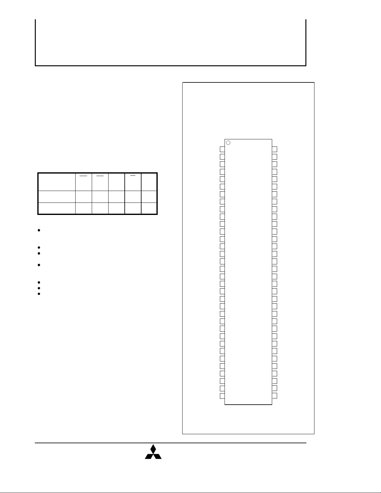
PIN CONFIGURATION ( TOP VIEW )
DQ1 1
DQ2 2
DQ3 3
DQ4 4
DQ5 5
Vss 6
DQ6 7
DQ7 8
DQ8 9
DQP1 10
DQ9 11
Vcc 12
DQ10 13
DQ11 14
DQ12 15
DQ13 16
DQ14 17
Vss 18
DQ15 19
DQ16 20
DQP2 21
Vcc 22
/CAS0 23
/CAS3 24
A0 25
A1 26
A2 27
Vss 28
A3 29
A4 30
A5 31
/RAS 32
A6 33
Vcc 34
68 DQP4
67 DQ32
66 DQ31
65 DQ30
64 DQ29
63 Vss
62 DQ28
61 DQ27
60 DQ26
59 DQ25
58 DQP3
57 Vcc
56 DQ24
55 DQ23
54 DQ22
53 DQ21
52 DQ20
51 Vss
50 DQ19
49 DQ18
48 DQ17
47 Vcc
46 /CAS2
45 /CAS1
44 /W
43 /OE
42 RFU(NC)
41 Vss
40 RFU(NC)
39 RFU(NC)
38 A9
37 A8
36 A7
35 Vcc
MIT-DS-0027-0.0 21 May 1996
MITSUBISHI
ELECTRIC
( / 18 )
1
Page 2
Preliminary Spec.
Some of contents are subject to change without notice.
FAST PAGE MODE 37748736-BIT ( 1048576-WORD BY 36-BIT ) DYNAMIC RAM
MITSUBISHI LSIs
MH1V36CAM-6,-7
FUNCTION
The MH1V36CAM provide, in addition to normal read,
write, and read-modify-write operations, a number of
other functions, e.g., fast page mode, RAS-only refresh, and
delayed-write. The input conditionsfor each are shown in Table 1.
Table 1 Input conditions for each mode
Operation
Read
Write (Early write)
Write (Delayed write)
Read-modify-write
RAS-only refresh
Hidden refresh
CAS before RAS refresh
Standby
Note : ACT : active, NAC : nonactive, DNC : don' t care, VLD : valid, IVD : Invalid,APD : applied, OPN : open
RAS CAS
ACT
ACT
ACT
ACT
ACT
ACT
ACT
NAC
ACT
ACT
ACT
ACT
NAC
ACT
ACT
DNC
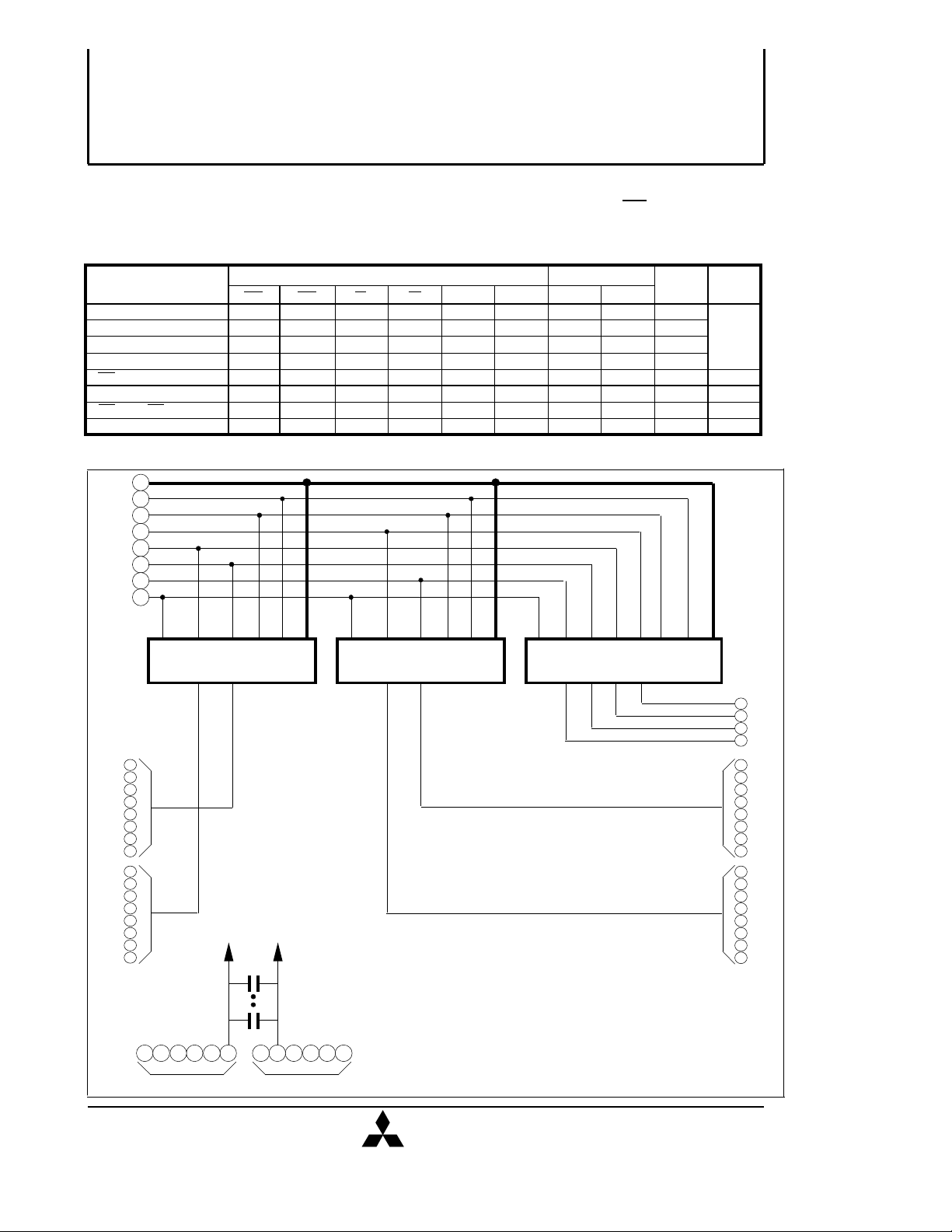
BLOCK DIAGRAM
Add
/W
/OE
/CAS3
/CAS2
/CAS1
/CAS0
/RAS
25,26,27,29,30,31,33,36,37,38
44
43
24
46
45
23
32
Inputs Input/Output
W
NAC
ACT
ACT
ACT
DNC
DNC
NAC
DNC
OE
ACT
DNC
DNC
ACT
DNC
ACT
DNC
DNC
Row
address address
APD
APD
APD
APD
APD
APD
DNC
DNC
Column
APD
APD
APD
APD
DNC
DNC
DNC
DNC
Input Output
OPN
VLD
VLD
VLD
DNC
OPN
DNC
DNC
VLD
OPN
IVD
VLD
OPN
VLD
OPN
OPN
Refresh Remark
YES
Fast page
YES
mode
YES
identical
YES
YES
YES
YES
NO
DQ9
DQ10
DQ11
DQ12
DQ13
DQ14
DQ15
DQ16
DQ17
DQ18
DQ19
DQ20
DQ21
DQ22
DQ23
DQ24
/LCAS
M5M4V18160C
11
13
14
15
16
17
19
20
48
49
50
52
53
54
55
56
C1 to C2
0.22 uF
57 6 18 2847
353422 41 51 6312
Add/OE /W/RAS /UCAS
/LCAS /CAS1/RAS
M5MV18160C
Add/OE /W/RAS /UCAS
DQ1 DQ2 DQ3 DQ4
/CAS3
/CAS2
/CAS4
M5M4V4500C
Add/OE /W
DQP4
68
DQP3
58
DQP2
21
DQP1
10
DQ1
01
DQ2
02
DQ3
03
DQ4
04
DQ5
05
DQ6
07
DQ7
08
DQ8
09
DQ25
59
DQ26
60
DQ27
61
DQ28
62
DQ29
64
DQ30
65
DQ31
66
DQ32
67
Vcc Vss
MIT-DS-0027-0.0 21 May 1996
MITSUBISHI
ELECTRIC
( / 18 )2
Page 3
Preliminary Spec.
Some of contents are subject to change without notice.
MITSUBISHI LSIs
MH1V36CAM-6,-7
FAST PAGE MODE 37748736-BIT ( 1048576-WORD BY 36-BIT ) DYNAMIC RAM
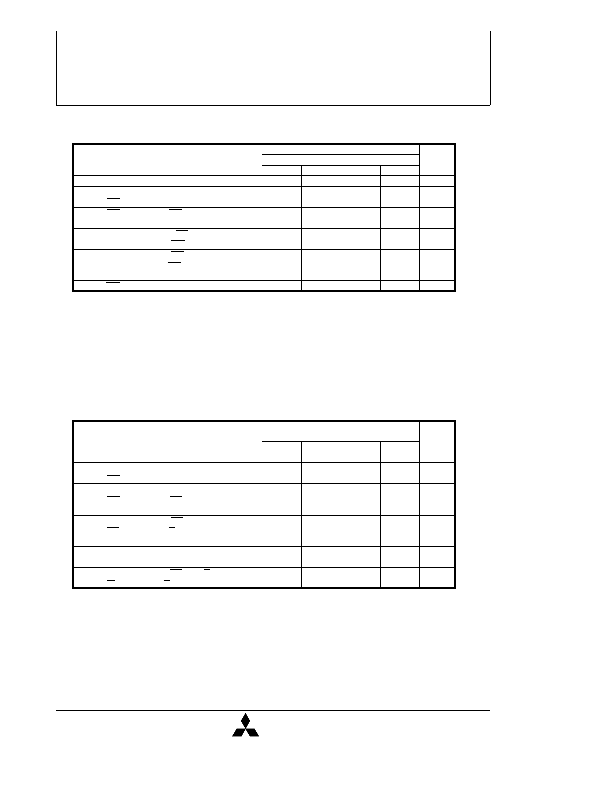
ABSOLUTE MAXIMUM RATINGS
Symbol
Vcc
VI
V0
I0
Pd
Topr
Tstg
Supply voltage
Input voltage
Output voltage
Output current
Power dissipation
Operating temperature
Storage temperature
RECOMMENDED OPERATING CONDITIONS
Symbol
Vcc
Vss
VIH
VIL
Note 1 : All voltage values are with respect to Vss
Supply voltage
Supply voltage
High-level input voltage, all inputs
Low-level input voltage, all inputs
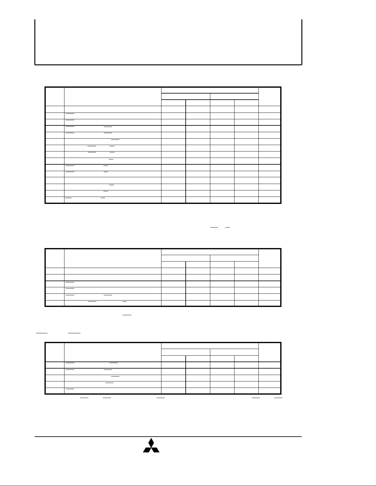
ELECTRICAL CHARACTERISTICS (Ta=0 ~70 °C, Vcc=3.3V+/- 0.3V, Vss=0V, unless otherwise noted) (Note 2)
Symbol
VOH
VOL
IOZ
I I
ICC1 (AV)
ICC2
ICC3 (AV)
ICC4(AV)
ICC6(AV)
Note 2: Current flowing into an IC is positive, out is negative.
3: Icc1 (AV), Icc3 (AV) , Icc4 (AV) and Icc6 (AV) are dependent on cycle rate. Maximum current is measured at the fastest cycle rate.
4: Icc1 (AV) and Icc4 (AV) are dependent on output loading. Specified values are obtained with the output open.
*: Column Address can be channged once or less while RAS=VIL and LCAS/UCAS=VIH
High-level output voltage
Low-level output voltage
Off-state output current
Input current
Average supply
current
from Vcc operating
Supply current from Vcc , stand-by
Average supply
current
from Vcc
refreshing
Average supply current
from Vcc
Fast-Page-Mode
Average supply current
from Vcc
CAS before RAS refresh
mode
CAPACITANCE
Symbol Parameter Test conditions
CI (A)
CI (OE)
CI (W)
CI (RAS)
CI (CAS)
CI / O
Input capacitance,
address inputs
Input capacitance, OE input
Input capacitance, write control input
Input capacitance, RAS input
Input capacitance, CAS input
Input/Output capacitance, data ports
Parameter Conditions Ratings Unit
-0.5 ~ 4.6
With respect to Vss
Ta=25°C
(Ta=0 ~70 °C , unless otherwise noted) (Note 1)
Parameter
Parameter
-6
(Note 3,4,*)
(Note 3,*)
(Note 3,4,*)
(Note 3,5,*)
(Ta=0~70°C , Vcc=3.3V+/-0.3V, Vss=0V, unless otherwise noted)
-7
-6
-7
-6
-7
-6
-7
Limits
Min Nom Max
3.0
0
2.0
-0.3
IOH=-2.0mA
IOL=2.0mA
Q floating 0V≤VOUT≤3.3V
0V≤VIN≤3.6V, Other inputs pins=0V
RAS, CAS cycling
tRC=tWC=min.
output open
RAS= CAS =VIH, output open
RAS= CAS≥Vcc -0.2V, output open
RAS cycling, CAS= VIH
tRC=min.
output open
RAS=VIL, CAS cycling
tPC=min.
output open
CAS before RAS refresh cycling
tRC=min.
output open
VI=Vss
f=1MHZ
Vi=25mVrms
3.3
0
Test conditions
3.6
0
Vcc+0.3
0.8
Unit
V
V
V
V
-0.5 ~ 4.6
-0.5 ~ 4.6
50
3
0 ~ 70
-40 ~ 100
Min Max
2.4
0
-10
-30
Limits
Typ
Min
Limits
Typ
Max
50
55
55
55
50
40
Vcc
0.4
10
30
380
330
6
1.5
380
330
210
190
370
320
V
V
V
mA
W
°C
°C
Unit
V
V
mA
mA
mA
mA
mA
Unit
pF
pF
pF
pF
pF
pF
MIT-DS-0027-0.0 21 May 1996
MITSUBISHI
ELECTRIC
( / 18 )3
Page 4
Preliminary Spec.
Some of contents are subject to change without notice.
FAST PAGE MODE 37748736-BIT ( 1048576-WORD BY 36-BIT ) DYNAMIC RAM
MITSUBISHI LSIs
MH1V36CAM-6,-7
SWITCHING CHARACTERISTICS
Symbol
Access time from CAS
tCAC
Access time from RAS
tRAC
Columu address access time
tAA
tCPA
Access time from CAS precharge
tOEA
Access time from OE
tCLZ
Output low impedance time from CAS low
Output disable time after CAS high
tOFF
tOEZ
Output disable time after OE high
Note 5: An initial pause of 500us is required after power-up followed by a minimum of eight initialization cycles (any combination of cycles
containing a RAS clock such as RAS-Only refresh).
Note the RAS may be cycled during the initial pause . And any 8 RAS or RAS/CAS cycles are required after prolonged periods
(greater than 16.4 ms) of RAS inactivity before proper device operation is achieved.
6: Measured with a load circuit equivalent to VOH=2.4V(IOH=-2mA)/VOL=0.4V(IOL=2mA) load 100pF.
The reference levels for measuring of output signal are 2.0V(VOH) and 0.8V(VOL).
7: Assumes that tRCDÅD≥tRCD(max) and tASC ≥tASC(max).
8: Assumes that tRCD ≤tRCD(max) and tRAD≤tRAD(max). If tRCD or tRAD is greater than the maximum recommended value shown in this table,
tRAC will increase by amount that tRCD exceeds the value shown.
9: Assumes that tRAD ≥tRAD(max) and tASC≤tASC(max).
10: Assumes that tCP ≤tCP(max) and tASC≥tASC(max).
11: tOFF(max) and tOEZ (max) defines the time at which the output achieves the high impedance state (IOUT ≤I +/- 10uAI) and is not reference to
VOH(min) or VOL(max).
Parameter
(Ta=0~70°C , Vcc=3.3V +/-0.3V, Vss=0V, unless otherwise noted , see notes 5,12,13)
Limits
(Note 6,7)
(Note 6,8)
(Note 6,9)
(Note 6,10)
(Note 6)
(Note 6)
(Note 11)
(Note 11)
-6 -7
Min Max Min Max
15
60
30
35
5
0
15
5
0
00 2015
20
70
35
40
2015
20
Unit
ns
ns
ns
ns
ns
ns
ns
ns
TIMING REQUIREMENTS (For Read, Write, Read-Modify-Write ,Refresh, and Fast-Page Mode Cycles)
(Ta=0 ~ 70 °C, Vcc=3.3V +/- 0.3V, Vss=0V, unless otherwise noted See notes 12,13)
16.4
45
30
10
50
Limits
Unit
16.4
50
20
10
0
10
15
0
0
10
15
0
0
20
1
50
35
10
50
ms
ns
ns
ns
ns
ns
ns
ns
ns
ns
ns
ns
ns
ns
ns
ns
Symbol
Refresh cycle time
tREF
RAS high pulse width
tRP
Delay time, RAS low to CAS low
tRCD
tCRP
Delay time, CAS high to RAS low
Delay time, RAS high to CAS low
tRPC
tCPN
CAS high pulse width
Column address delay time from RAS low
tRAD
tASR
Row address setup time before RAS low
Column address setup time before CAS low
tASC
Row address hold time after RAS low
tRAH
tCAH
Column address hold time after CAS low
tDZC
Delay time, data to CAS low
tDZO
Delay time, data to OE low
Delay time, CAS high to data
tCDD
tODD
Delay time, OE high to data
tT
Transition time
Note 12: The timing requirements are assumed tT =5ns.
13: VIH(min) and VIL(max) are reference levels for measuring timing of input signals.
14: tRCD(max) is specified as a reference point only. If tRCD is less than tRCD(max), access time is tRAC. If tRCD is greater than tRCD(max), access
time is controlled exclusively by tCAC or tAA. tRCD(min) is specified as tRCD(min) =tRAH(min) +2tH+tASC(min).
15: tRAD(max) is specified as a reference point only. If tRAD≥tRAD(max) and tASC≤tASC(max), access time is controlled exclusively by tAA.
16: tASC(max) is specified as a reference point only. If tRCD≥tRCD(max) and tASC≥tASC(max), access time is controlled exclusively by tCAC.
17: Either tDZC or tDZO must be satisfied.
18: Either tCDD or tODD must be satisfied.
19: tT is measured between VIH(min) and VIL(max).
Parameter
(Note14)
(Note15)
(Note16)
(Note17)
(Note17)
(Note18)
(Note18)
(Note19)
-6 -7
Min Max Min Max
40
20
10
0
10
15
0
0
10
15
0
0
15
15 20
1
MIT-DS-0027-0.0 21 May 1996
MITSUBISHI
ELECTRIC
( / 18 )
4
Page 5
Preliminary Spec.
Some of contents are subject to change without notice.
FAST PAGE MODE 37748736-BIT ( 1048576-WORD BY 36-BIT ) DYNAMIC RAM
Read and Refresh Cycles
Symbol
Read cycle time
tRC
RAS low pulse width
tRAS
CAS low pulse width
tCAS
tCSH
CAS hold time after RAS low
tRSH
RAS hold time after CAS low
tRCS
Read Setup time after CAS high
Read hold time after CAS low
tRCH
tRRH
Read hold time after RAS low
tRAL
Column address to RAS hold time
tOCH
CAS hold time after OE low
tORH
RAS hold time after OE low
Note 20: Either tRCH or tRRH must be satisfied for a read cycle.
Parameter
(Note 20)
(Note 20)
MITSUBISHI LSIs
MH1V36CAM-6,-7
Limits
-6 -7
Min Max Min Max
110
60
15
60
15
10
30
15
15
10000
10000
0
0
130
20
70
20
10
35
20
20
70
10000
10000
0
0
Unit
ns
ns
ns
ns
ns
ns
ns
ns
ns
ns
ns
Write Cycle (Early Write and Delayed Write)
Symbol
tWC
tRAS
tCAS
tCSH
tRSH
tWCS
tWCH
tCWL
tRWL
tWP
tDS
tDH
tOEH
Write cycle time
RAS low pulse width
CAS low pulse width
CAS hold time after RAS low
RAS hold time after CAS low
Write setup time before CAS low
Write hold time after CAS low
CAS hold time after W low
RAS hold time after W low
Write pulse width
Data setup time before CAS low or W low
Data hold time after CAS low or W low
OE hold time after W low
Parameter
(Note 22)
Limits
-6 -7
Min Max Min Max
110
60
15
60
15
15
15
10
0
10
15
10000
10000
0
10
130
70
20
70
20
20
20
15
0
15
20
10000
10000
0
15
Unit
ns
ns
ns
ns
ns
ns
ns
ns
ns
ns
ns
ns
ns
MIT-DS-0027-0.0 21 May 1996
MITSUBISHI
ELECTRIC
( / 18 )
5
Page 6
Preliminary Spec.
Some of contents are subject to change without notice.
MITSUBISHI LSIs
MH1V36CAM-6,-7
FAST PAGE MODE 37748736-BIT ( 1048576-WORD BY 36-BIT ) DYNAMIC RAM
Read-Write and Read-Modify-Write Cycles
10000
10000
Limits
120
120
95
Unit
ns
10000
70
70
0
45
60
20
20
15
0
10000
ns
ns
ns
ns
ns
ns
ns
ns
ns
ns
ns
ns
ns
Symbol
Read write/read modify write cycle time
tRWC
RAS low pulse width
tRAS
CAS low pulse width
tCAS
tCSH
CAS hold time after RAS low
RAS hold time after CAS low
tRSH
tRCS
Read setup time before CAS low
tCWD
Delay time, CAS low to W low
tRWD
Delay time, RAS low to W low
tAWD
Delay time, address to W low
tCWL
CAS hold time after W low
tRWL
RAS hold time after W low
tWP
Write pulse width
tDS
Data setup time before W low
Data hold time after W low
tDH
tOEH
OE hold time after W low
Note 21: tRWC is specified as tRWC(min)=tRAC(max)+tODD(min)+tRWL(min)+tRP(min)+5tT.
22: tWCS, tCWD,tRWD and tAWD and,tCPWD are specified as reference points only. If tWCS≥tWCS(min) the cycle is an early write cycle and the
DQ pins will remain high impedance throughout the entire cycle. If tCWD≥tCWD(min), tRWD≥tRWD (min), tAWD≥tAWD(min) and tCPWD≥tCPWD(min)
(for fast page mode cycle only), the cycle is a read-modify-write cycle and the DQ will contain the data read from the selected address.
If neither of the above condition (delayed write) of the DQ (at access time and until CAS or OE goes back to VIH ) is indeterminate.
Parameter
(Note21)
(Note22) ns
(Note22)
(Note22)
ÅÜ ÅÜ
ÅÖ ÅÖ
-6 -7
Min Max Min Max
155 180
105
60
105
60
0
40
85
55
15
15
10
0
10 15
15 20
Fast-Page Mode Cycle (Read, Early Write, Read -Write, Read-Modify-Write Cycle) (Note 23)
Limits
Symbol
Fast page mode read/write cycle time
tPC
Fast page mode read write/read modify write cycle time
tPRWC
RAS low pulse width for read write cycle
tRAS
CAS high pulse width
tCP
RAS hold time after CAS precharge
tCPRH
tCPWD
Delay time, CAS precharge to W low
Note 23: All previously specified timing requirements and switching characteristics are applicable to their respective fast page mode cycle.
24: tRAS(min) is specified as two cycles of CAS input are performed.
25: tCP(max) is specified as a reference point only.
Parameter
(Note24)
(Note25)
(Note22)
-6 -7
Min Max Min Max
40
85
100
10
35
60
100000
15
45
95
115
65
100000
10
40
15
Unit
ns
ns
ns
ns
ns
ns
CAS before RAS Refresh Cycle (Note 26)
Symbol
CAS setup time before RAS low
tCSR
tCHR
CAS hold time after RAS low
tRSR
Read setup time before RAS low
tRHR
Read hold time after RAS low
tCAS 25
CAS low pulse width
Note 26: Eight or more CAS before RAS cycles instead of eight RAS cycles are necessary for proper operation of CAS before RAS refresh
mode.
Parameter
-6 -7
Min Max Min Max
10
10
10
10
Limits
10
10
30
Unit
ns
15
15
ns
ns
ns
ns
MIT-DS-0027-0.0 21 May 1996
MITSUBISHI
ELECTRIC
( / 18 )
6
Page 7

Preliminary Spec.
Some of contents are subject to change without notice.
FAST PAGE MODE 37748736-BIT ( 1048576-WORD BY 36-BIT ) DYNAMIC RAM
Timing Diagrams (Note 27)
Read Cycle
MITSUBISHI LSIs
MH1V36CAM-6,-7
tRC
RAS
CAS
A0 ~ A9
W
DQ
(INPUTS)
DQ
(OUTPUTS)
OE
VIH
VIL
VIH
VIL
VIH
VIL
VIH
VIL
VIH
VIL
VOH
VOL
VIH
VIL
tRAS
tCSH
tCRP
tASR
tRAH
ROW COLUMN
ADDRESS ADDRESS
tRCD
tRAD
tASC
tRCS
tDZC
tRAC
tDZO
tCAH
tCAC
tAA
tCLZ
tCAS
tRAL
tRSH
Hi-Z
tOEA
tOCH
tOFF
DATA VALID
tRP
tCRPtRPC
tASR
tCPN
ROW
ADDRESS
tRRH
tRCH
tCDD
Hi-ZHi-Z
tOEZ
tODD
tORH
Note 27
Indicates the don't care input.
VIH(min)≤VIN≤VIH(max) or VIL(min)≤VIN≤VIL(max)
Indicates the invalid output.
Indicates the skew of the four inputs.
MIT-DS-0027-0.0 21 May 1996
MITSUBISHI
ELECTRIC
( / 18 )
7
Page 8

Preliminary Spec.
Some of contents are subject to change without notice.
FAST PAGE MODE 37748736-BIT ( 1048576-WORD BY 36-BIT ) DYNAMIC RAM
Write Cycle (Early write)
MITSUBISHI LSIs
MH1V36CAM-6,-7
tWC
RAS
CAS
A0 ~ A9
W
DQ
(INPUTS)
VIH
VIL
VIH
VIL
VIH
VIL
VIH
VIL
VIH
VIL
tCRP
tASR
tRAH
ROW COLUMN
ADDRESS ADDRESS
tRCD
tASC
tWCS
tDS
tRAS
tCSH
tCAH
tWCH
tDH
DATA VALID
tCAS
tRSH
tRPC
tRP
tCRP
tASR
ROW
ADDRESS
DQ
(OUTPUTS)
OE
MIT-DS-0027-0.0 21 May 1996
VOH
VOL
VIH
VIL
Hi-Z
MITSUBISHI
ELECTRIC
( / 18 )
8
Page 9

Preliminary Spec.
Some of contents are subject to change without notice.
FAST PAGE MODE 37748736-BIT ( 1048576-WORD BY 36-BIT ) DYNAMIC RAM
Write Cycle (Delayed write)
MITSUBISHI LSIs
MH1V36CAM-6,-7
tWC
RAS
CAS
A0 ~ A9
W
DQ
(INPUTS)
VIH
VIL
VIH
VIL
VIH
VIL
VIH
VIL
VIH
VIL
tCRP
tASR tRAH
ROW COLUMN
ADDRESS ADDRESS
tRCD
tASC
tRCS
tCSH
tDZC
tCLZ
tRAS
Hi-Z
tCAH
tRSH
tCAS
tWCH
tDS
tCWL
tWP
tDH
DATA
VALID
tRWL
tRPC
tRP
tCRP
tASR
ROW
ADDRESS
DQ
(OUTPUTS)
OE
MIT-DS-0027-0.0 21 May 1996
VOH
VOL
VIH
VIL
Hi-Z
tDZO
tOEZ
MITSUBISHI
Hi-Z
tOEH
tODD
ELECTRIC
( / 18 )
9
Page 10

Preliminary Spec.
Some of contents are subject to change without notice.
FAST PAGE MODE 37748736-BIT ( 1048576-WORD BY 36-BIT ) DYNAMIC RAM
Read-Write, Read-Modify-Write Cycle
MITSUBISHI LSIs
MH1V36CAM-6,-7
tRWC
RAS
CAS
A0 ~ A9
W
DQ
(INPUTS)
DQ
(OUTPUTS)
VIH
VIL
VIH
VIL
VIH
VIL
VIH
VIL
VIH
VIL
VOH
VOL
tCRP
tRCD
tRAD
tASR
tRAH
ROW COLUMN
ADDRESS ADDRESS
Hi-Z
tASC
tRCS
tDZC
tRAC
tDZO
tCAC
tAA
tCLZ
tCSH
Hi-Z
tOEA
tRAS
tCAH
tAWD
tCWD
tRWD
DATA
VALID
tCAS
tOEZ
tRSH
tODD
tDS
tCWL
tRWL
tWP
tDH
DATA VALID
tOEH
Hi-Z
tRPC
tRP
tCRP
tASR
ROW
ADDRESS
OE
MIT-DS-0027-0.0 21 May 1996
VIH
VIL
MITSUBISHI
ELECTRIC
( / 18 )
10
Page 11

Preliminary Spec.
Some of contents are subject to change without notice.
FAST PAGE MODE 37748736-BIT ( 1048576-WORD BY 36-BIT ) DYNAMIC RAM
RAS-only Refresh Cycle
RAS
VIH
VIL
tRAS
MITSUBISHI LSIs
MH1V36CAM-6,-7
tRC
tRP
CAS
A0 ~ A9
W
DQ
(INPUTS)
DQ
(OUTPUTS)
VIH
VIL
VIH
VIL
VIH
VIL
VIH
VIL
VOH
VOL
tCRP
tASR
tRAH
ROW
ADDRESS
Hi-Z
tRPC
tCRP
tASR
ROW
ADDRESS
OE
MIT-DS-0027-0.0 21 May 1996
VIH
VIL
MITSUBISHI
ELECTRIC
( / 18 )
11
Page 12

Preliminary Spec.
Some of contents are subject to change without notice.
FAST PAGE MODE 37748736-BIT ( 1048576-WORD BY 36-BIT ) DYNAMIC RAM
CAS before RAS Refresh Cycle
MITSUBISHI LSIs
MH1V36CAM-6,-7
RAS
CAS
A0 ~ A9
W
DQ
(INPUTS)
DQ
(OUTPUTS)
OE
VIH
VIL
VIH
VIL
VIH
VIL
VIH
VIL
VIH
VIL
VOH
VOL
VIH
VIL
tRP
tCSR
tRPC
tCPN
tRCH tRSR
tOFF
tOEZ
tCHR
tRHR
tRAS
tRC
tCSRtRPC
tRSR
tCHR
tRHR
Hi-Z
tRAS
tRC
tRPC
tRP
tCRP
tASR
ROW
ADDRESS
COLUMN
ADDRESS
tRCS
MIT-DS-0027-0.0 21 May 1996
MITSUBISHI
ELECTRIC
( / 18 )
12
Page 13

Preliminary Spec.
Some of contents are subject to change without notice.
FAST PAGE MODE 37748736-BIT ( 1048576-WORD BY 36-BIT ) DYNAMIC RAM
Hidden Refresh Cycle (Read) (Note 28)
MITSUBISHI LSIs
MH1V36CAM-6,-7
RAS
CAS
A0 ~ A9
W
DQ
(INPUTS)
DQ
(OUTPUTS)
OE
VIH
VIL
VIH
VIL
VIH
VIL
VIH
VIL
VIH
VIL
VOH
VOL
VIL
VIH
tCRP
tASR
tRAH
ROW
ADDRESS
tRC
tRAS
tRCD
tRAD
tASC
tRCS
tDZC tCDD
Hi-Z
tRAC
tDZO tOEA
tRSH
tCAH
COLUMN
ADDRESS
tRAL
tCAC
tAA
tCLZ
tORH
tRP
tCHR
tRRH
Hi-Z
DATA VALID
tRC
tRAS
tOEZ
tRP
tASR
ROW
ADDRESS
tOFF
Hi-Z
tODD
Note 28: Early write, delayed write, read write or read modify write cycle is applicable instead of read cycle.
Timing requirements and output state are the same as that of each cycle shown above.
MIT-DS-0027-0.0 21 May 1996
MITSUBISHI
ELECTRIC
( / 18 )
13
Page 14

Preliminary Spec.
Some of contents are subject to change without notice.
FAST PAGE MODE 37748736-BIT ( 1048576-WORD BY 36-BIT ) DYNAMIC RAM
Fast Page Mode Read Cycle
MITSUBISHI LSIs
MH1V36CAM-6,-7
RAS
CAS
A0 ~ A9
W
DQ
(INPUTS)
DQ
(OUTPUTS)
OE
VIH
VIL
VIH
VIL
VIH
VIL
VIH
VIL
VIH
VIL
VOH
VOL
VIL
VIH
tCRP
tASR
ADDRESS
ROW
tRAH
Hi-Z
tRCD
tRAD
tCSH
tASC
COLUMN-1
tRCS
tDZC
tRAC
tDZO tOEA
tCAH
tCAC
tAA
Hi-Z
tCLZ
tCAS
tOCH
tRCH
tOFF
DATA
VALID-1
tRAS
tPC
tCP
tASC
COLUMN-2 COLUMN-3
tODD
tCAS tCP tCAS
tCAH
tRCS
tRCH
tDZC
Hi-Z
tCAC
tAA
tCLZ
DATA
VALID-2
tCPA
tOEA
tOEZ
tOCH
tDZO
tCPRH
tASC
tDZC
tOFF
tOEZ
tODD
tRCS
tCPA
tDZO
tRSH
tCAH
tRAL
tAA
tCLZ
tCAC
tOEA
tOCH
tORH
tRP
tASR
ROW
ADDRESS
tRRH
tRCH
tCDD
tOFF
DATA
VALID-3
tOEZ
tODD
MIT-DS-0027-0.0 21 May 1996
MITSUBISHI
ELECTRIC
( / 18 )
14
Page 15

Preliminary Spec.
Some of contents are subject to change without notice.
FAST PAGE MODE 37748736-BIT ( 1048576-WORD BY 36-BIT ) DYNAMIC RAM
Fast Page Mode Write Cycle (Early Write)
MITSUBISHI LSIs
MH1V36CAM-6,-7
RAS
CAS
A0 ~ A9
W
DQ
(INPUTS)
VIH
VIL
VIH
VIL
VIH
VIL
VIH
VIL
VIH
VIL
tCRP
tASR tRAH
ROW
ADDRESS
tCSH tPC
tRCD
tASC
tWCS
tDS
tCAS
tCAH
COLUMN-1
tDH
DATA
VALID-1
tRAS
tCP
tASC
tDS tDH tDS tDH
tCAS tCP
tCAH
COLUMN-2
tWCH
DATA
VALID-2
tASC
COLUMN-3
VALID-3
DATA
tRSH
tCAS
tCAH
tWCHtWCH tWCS tWCS
tRP
tASR
ROW
ADDRESS
DQ
(OUTPUTS)
OE
MIT-DS-0027-0.0 21 May 1996
VOH
VOL
VIH
VIL
Hi-Z
MITSUBISHI
ELECTRIC
( / 18 )
15
Page 16

Preliminary Spec.
Some of contents are subject to change without notice.
FAST PAGE MODE 37748736-BIT ( 1048576-WORD BY 36-BIT ) DYNAMIC RAM
Fast-Page Mode Write Cycle (Delayed Write)
MITSUBISHI LSIs
MH1V36CAM-6,-7
RAS
CAS
A0 ~ A9
W
DQ
(INPUTS)
VIH
VIL
VIH
VIL
VIH
VIL
VIH
VIL
VIH
VIL
tCRP
tASR
ADDRESS
ROW
tRAH
tRCD
tASC
tRAS
tCSH
tCAS
tCAH
COLUMN-1
tWCH
tDS
tCWL
tWP
tDH
DATA
VALID-1
tRCS
tDZC
Hi-Z Hi-Z
tCP
COLUMN-2
tRCS
tDZC
tRP
tRSH
tPC
tCAS
tCAHtASC
tRWL
tWCH
tDS
tCWL
tWP
tDH
DATA
VALID-2
tASR
ROW
ADDRESS
tCLZ tCLZ
DQ
(OUTPUTS)
OE
MIT-DS-0027-0.0 21 May 1996
VOH
VOL
VIH
VIL
Hi-Z
tDZO
tOEZ
tODD tDZO
MITSUBISHI
Hi-Z Hi-Z
tOEZ
tOEH
tODD
ELECTRIC
( / 18 )
16
Page 17

Preliminary Spec.
Some of contents are subject to change without notice.
FAST PAGE MODE 37748736-BIT ( 1048576-WORD BY 36-BIT ) DYNAMIC RAM
Fast Page Mode Read-Write,Read-Modify-Write Cycle
MITSUBISHI LSIs
MH1V36CAM-6,-7
RAS
CAS
A0 ~ A9
W
DQ
(INPUTS)
DQ
(OUTPUTS)
OE
VIH
VIL
VIH
VIL
VIH
VIL
VIH
VIL
VIH
VIL
VOH
VOL
VIH
VIL
tCRP
tASR
ADDRESS
ROW
tRAH
Hi-Z
tRCD
tRAD
tASC
tRAS
tCSH
tCAS
tCAH
COLUMN-1
tAWD tAWD
tRCS
tDZC
tAA
tCLZ
tRAC
tDZO
tCWD
tRWD
Hi-Z Hi-Z
tCAC
DATA
VALID-1
tOEA
tCWL
tWP
tDS
DATA
VALID-1
Hi-Z Hi-Z
tODD
tOEZ
tPRWC
tCP
tASC
COLUMN-2
tRCS
tDZC
tDH
tCAC
tAA
tCPA
tDZO tOEZ
tOEA
tCAH
tCWD
tCPWD
tCLZ
VALID-1
tCAS
DATA
tDS
tODD
tRWL
tCWL
tWP
tDH
DATA
VALID-2
tOEH
tRP
tASR
ROW
ADDRESS
MIT-DS-0027-0.0 21 May 1996
MITSUBISHI
ELECTRIC
( / 18 )
17
Page 18

Preliminary Spec.
Some of contents are subject to change without notice.
FAST PAGE MODE 37748736-BIT ( 1048576-WORD BY 36-BIT ) DYNAMIC RAM
MH1V36CAM OUTLINE
MITSUBISHI LSIs
MH1V36CAM-6,-7
No mounted area
11mm x 11mm
21
12.5
10.5
58
29
68 35
11mm
11mm
1 34
1
0.5
33 x 1 = 33
3.5MAX
24
A
1
1
:0°~5°
1.2
1.0
1.5
2.55
Detail A
MIT-DS-0027-0.0 21 May 1996
MITSUBISHI
ELECTRIC
( / 18 )
18
 Loading...