

Page 1
SEMICONDUCTOR TECHNICAL DATA
N–Channel Enhancement–Mode Silicon Gate
Order this document
by MGP7N60E/D
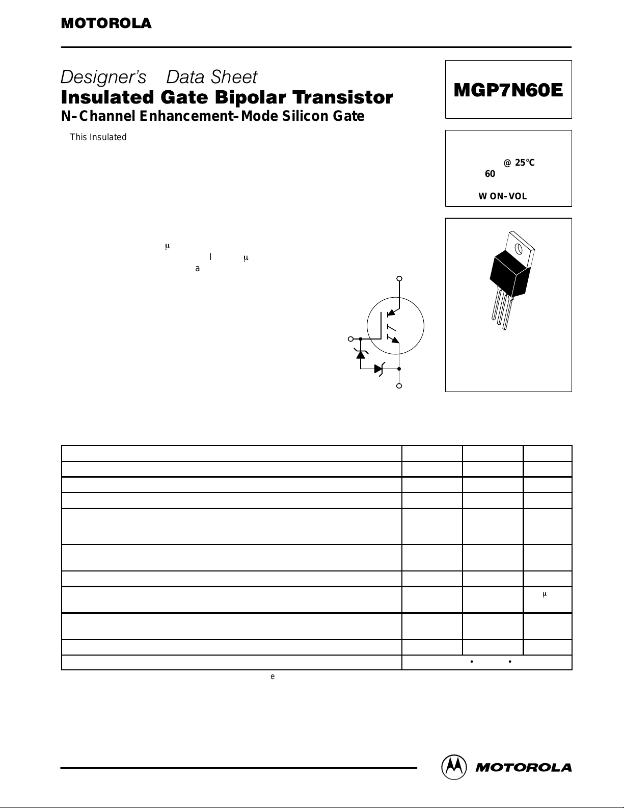
This Insulated Gate Bipolar Transistor (IGBT) uses an advanced
termination scheme to provide an enhanced and reliable high
voltage–blocking capability. Its new 600 V IGBT technology is
specifically suited for applications requiring both a high temperature short circuit capability and a low V
. It also provides fast
CE(on)
switching characteristics and results in efficient operation at high
frequencies. This new E–series introduces an energy efficient,
ESD protected, and short circuit rugged device.
• Industry Standard TO–220 Package
• High Speed: E
= 70 mJ/A typical at 125°C
off
• High Voltage Short Circuit Capability – 10 ms minimum at 125°C, 400 V
• Low On–Voltage 2.0 V typical at 5.0 A, 125°C
• Robust High Voltage Termination
• ESD Protection Gate–Emitter Zener Diodes
G
IGBT IN TO–220
7.0 A @ 90°C
10 A @ 25°C
600 VOL TS
SHORT CIRCUIT RATED
LOW ON–VOLTAGE
C
G
C
E
CASE 221A–09
STYLE 9
E
TO–220AB
MAXIMUM RATINGS
Collector–Emitter Voltage V
Collector–Gate Voltage (RGE = 1.0 MΩ) V
Gate–Emitter Voltage — Continuous V
Collector Current — Continuous @ TC = 25°C
Collector Current — Continuous @ TC = 90°C
Collector Current — Repetitive Pulsed Current (1)
Total Power Dissipation @ TC = 25°C
Derate above 25°C
Operating and Storage Junction Temperature Range TJ, T
Short Circuit Withstand Time
(VCC = 400 Vdc, VGE = 15 Vdc, TJ = 125°C, RG = 20 Ω)
Thermal Resistance — Junction to Case – IGBT
Thermal Resistance — Junction to Ambient
Maximum Lead Temperature for Soldering Purposes, 1/8″ from case for 5 seconds T
Mounting Torque, 6–32 or M3 screw
(1) Pulse width is limited by maximum junction temperature. Repetitive rating.
Designer’s Data for “Worst Case” Conditions — The Designer’s Data Sheet permits the design of most circuits entirely from the information presented. SOA Limit
curves — representing boundaries on device characteristics — are given to facilitate “worst case” design.
Designer’s is a trademark of Motorola, Inc.
(TJ = 25°C unless otherwise noted)
Rating Symbol Value Unit
CES
CGR
GE
I
C25
I
C90
I
CM
P
D
stg
t
sc
R
θJC
R
θJA
L
10 lbfSin (1.13 NSm)
600 Vdc
600 Vdc
±20 Vdc
10
7.0
14
81
0.65
–55 to 150 °C
10
1.5
65
260 °C
Adc
Apk
Watts
W/°C
m
°C/W
s
Motorola IGBT Device Data
Motorola, Inc. 1998
1
Page 2
MGP7N60E
)
f = 1.0 MHz)
)
R
G
Ω)
)
R
G
T
J
125 C)
)
V
GE
Vdc)
ELECTRICAL CHARACTERISTICS
OFF CHARACTERISTICS
Collector–to–Emitter Breakdown Voltage
(VGE = 0 Vdc, IC = 25 µAdc)
T emperature Coef ficient (Positive)
Emitter–to–Collector Breakdown Voltage (VGE = 0 Vdc, IEC = 100 mAdc) V
Zero Gate Voltage Collector Current
(VCE = 600 Vdc, VGE = 0 Vdc)
(VCE = 600 Vdc, VGE = 0 Vdc, TJ = 125°C)
Gate–Body Leakage Current (VGE = ± 20 Vdc, VCE = 0 Vdc) I
ON CHARACTERISTICS (1)
Collector–to–Emitter On–State Voltage
(VGE = 15 Vdc, IC = 2.5 Adc)
(VGE = 15 Vdc, IC = 2.5 Adc, TJ = 125°C)
(VGE = 15 Vdc, IC = 5.0 Adc)
Gate Threshold Voltage
(VCE = VGE, IC = 1.0 mAdc)
Threshold Temperature Coefficient (Negative)
Forward Transconductance (VCE = 10 Vdc, IC = 5.0 Adc) g
DYNAMIC CHARACTERISTICS
Input Capacitance
Output Capacitance
Transfer Capacitance
SWITCHING CHARACTERISTICS (1)
Turn–On Delay Time
Rise Time
Turn–Off Delay Time
Fall Time
Turn–Off Switching Loss E
Turn–On Delay Time
Rise Time
Turn–Off Delay Time
Fall Time
Turn–Off Switching Loss E
Gate Charge
INTERNAL PACKAGE INDUCTANCE
Internal Emitter Inductance
(Measured from the emitter lead 0.25″ from package to emitter bond pad)
(1) Pulse Test: Pulse Width ≤ 300 µs, Duty Cycle ≤ 2%.
(T
= 25°C unless otherwise noted)
J
Characteristic
(VCE = 25 Vdc, VGE = 0 Vdc,
(VCC = 360 Vdc, IC = 5.0 Adc,
VGE = 15 Vdc, L = 300 mH,
Energy losses include “tail”
(VCC = 360 Vdc, IC = 5.0 Adc,
VGE = 15 Vdc, L = 300 mH,
Energy losses include “tail”
(VCC = 360 Vdc, IC = 5.0 Adc,
R
= 20 Ω, T
= 20 Ω,
f = 1.0 MHz
R
= 20 Ω
= 20
V
= 15 Vdc
= 15
= 125°C
=
Symbol Min Typ Max Unit
V
(BR)CES
(BR)ECS
I
CES
GES
V
CE(on)
V
GE(th)
fe
C
ies
C
oes
C
res
t
d(on)
t
r
t
d(off)
t
f
off
t
d(on)
t
r
t
d(off)
t
f
off
Q
T
Q
1
Q
2
L
E
600
—
15 — — Vdc
—
—
— — 50
—
—
—
4.0
—
— 2.5 — Mhos
— 610 —
— 60 —
— 10 —
— 22 —
— 24 —
— 64 —
— 196 —
— 0.20 0.34 mJ
— 31 —
— 24 —
— 195 —
— 220 —
— 0.35 — mJ
— 27.2 —
— 7.0 —
— 13.7 —
— 7.5 —
—
870
—
—
1.6
1.5
2.0
6.0
10
—
—
10
200
1.9
—
2.4
8.0
—
mV/°C
µAdc
m
mV/°C
Vdc
Adc
Vdc
Vdc
pF
ns
ns
nC
nH
2
Motorola IGBT Device Data
Page 3

20
TJ = 25°C
20 V
17.5 V
15 V
20
TJ = 125°C
20 V
17.5 V
MGP7N60E
15 V
15
12.5 V
10
5
, COLLECTOR CURRENT (AMPS)
C
I
0
312 4567
VCE, COLLECTOR–TO–EMITTER VOLTAGE (VOL TS)
VGE = 10 V
80
Figure 1. Output Characteristics Figure 2. Output Characteristics
12
10 2.0
, COLLECTOR CURRENT (AMPS)
C
I
8
6
4
2
0
VCE = 100 V
5
m
S PULSE WIDTH
TJ = 125°C
25°C
6789 25 50 75 100 125 150
VGE, GATE–T O–EMITTER VOLTAGE (VOLTS)
10 125
13
15
10
, COLLECTOR CURRENT (AMPS)
C
I
2.2
1.8
1.6
1.4
VOLTAGE (VOLTS)
, COLLECTOR–TO–EMITTER ON–STATE
1.2
CE(on)
1.0
V
5
0
VCE, COLLECTOR–TO–EMITTER VOLTAGE (VOL TS)
VGE = 15 V
80
m
–25–50
312 4567
S PULSE WIDTH
011
TJ, JUNCTION TEMPERATURE (
12.5 V
VGE = 10 V
IC = 5.0 A
3.75 A
2.5 A
°
C)
80
C, CAPACITANCE (pF)
1200
1000
800
600
400
200
Figure 3. Transfer Characteristics Figure 4. VCE versus Junction T emperature
C
ies
C
oes
C
0
5
VCE, COLLECTOR–TO–EMITTER VOLTAGE (VOL TS)
res
100
Figure 5. Capacitance Variation Figure 6. VGE versus T otal Charge
VGE = 0 V
TJ = 25
15 2520
20
°
C
, GATE–T O–EMITTER VOLTAGE (VOLTS)
GE
V
16
12
Q1 Q2
8
4
0
QT
TJ = 25°C
IC = 5.0 A
10 15 3520 25
5300
Qg, TOTAL GATE CHARGE (nC)
Motorola IGBT Device Data
3
Page 4

MGP7N60E
0.5
VCC = 360 V
VGE = 15 V
TJ = 125
0.4
0.5
VCC = 360 V
°
C
IC = 5.0 A
0.4
VGE = 15 V
RG = 20
W
IC = 5.0 A
0.3
0.2
0.1
, TURN–OFF ENERGY LOSSES (mJ)E
off
0
0.6
0.5
0.4
0.3
0.2
, TURN–OFF ENERGY LOSSES (mJ)
0.1
off
E
0
3.75 A
2.5 A
2515 20 30 35 40 45
GATE RESISTANCE (OHMS)
5010
Figure 7. T urn–Off Losses versus Gate
Resistance
VCC = 360 V
VGE = 15 V
RG = 20
W
TJ = 125°C
1234 10 100 1000
I
, COLLECTOR CURRENT (AMPS)
C
570
6
8
0.3
0.2
0.1
, TURN–OFF ENERGY LOSSES (mJ)E
off
0
100
10
, COLLECTOR CURRENT (AMPS)
C
I
1
3.75 A
2.5 A
5025 75 100 125
TJ, JUNCTION TEMPERATURE (
°
C)
Figure 8. T urn–Off Losses versus Junction
T emperature
VGE = 15 V
RGE = 20
TJ = 125°C
1
W
VCE, COLLECTOR–TO–EMITTER VOLTAGE (VOL TS)
1500
Figure 9. T urn–Off Energy Losses versus
Collector Current
Figure 10. Reverse Biased Safe Operating
Area
4
Motorola IGBT Device Data
Page 5

P ACKAGE DIMENSIONS
MGP7N60E
SEATING
–T–
PLANE
B
4
Q
123
F
T
A
U
C
S
H
K
Z
L
V
R
J
G
D
N
NOTES:
1. DIMENSIONING AND TOLERANCING PER ANSI
Y14.5M, 1982.
2. CONTROLLING DIMENSION: INCH.
3. DIMENSION Z DEFINES A ZONE WHERE ALL
BODY AND LEAD IRREGULARITIES ARE
ALLOWED.
DIM MIN MAX MIN MAX
A 0.570 0.620 14.48 15.75
B 0.380 0.405 9.66 10.28
C 0.160 0.190 4.07 4.82
D 0.025 0.035 0.64 0.88
F 0.142 0.147 3.61 3.73
G 0.095 0.105 2.42 2.66
H 0.110 0.155 2.80 3.93
J 0.018 0.025 0.46 0.64
K 0.500 0.562 12.70 14.27
L 0.045 0.060 1.15 1.52
N 0.190 0.210 4.83 5.33
Q 0.100 0.120 2.54 3.04
R 0.080 0.110 2.04 2.79
S 0.045 0.055 1.15 1.39
T 0.235 0.255 5.97 6.47
U 0.000 0.050 0.00 1.27
V 0.045 ––– 1.15 –––
Z ––– 0.080 ––– 2.04
STYLE 9:
PIN 1. GATE
MILLIMETERSINCHES
2. COLLECTOR
3. EMITTER
4. COLLECTOR
CASE 221A–09
TO–220AB
ISSUE Z
Motorola reserves the right to make changes without further notice to any products herein. Motorola makes no warranty , representation or guarantee regarding
the suitability of its products for any particular purpose, nor does Motorola assume any liability arising out of the application or use of any product or circuit, and
specifically disclaims any and all liability, including without limitation consequential or incidental damages. “T ypical” parameters which may be provided in Motorola
data sheets and/or specifications can and do vary in different applications and actual performance may vary over time. All operating parameters, including “Typicals”
must be validated for each customer application by customer’s technical experts. Motorola does not convey any license under its patent rights nor the rights of
others. Motorola products are not designed, intended, or authorized for use as components in systems intended for surgical implant into the body, or other
applications intended to support or sustain life, or for any other application in which the failure of the Motorola product could create a situation where personal injury
or death may occur. Should Buyer purchase or use Motorola products for any such unintended or unauthorized application, Buyer shall indemnify and hold Motorola
and its officers, employees, subsidiaries, affiliates, and distributors harmless against all claims, costs, damages, and expenses, and reasonable attorney fees
arising out of, directly or indirectly, any claim of personal injury or death associated with such unintended or unauthorized use, even if such claim alleges that
Motorola was negligent regarding the design or manufacture of the part. Motorola and are registered trademarks of Motorola, Inc. Motorola, Inc. is an Equal
Opportunity/Affirmative Action Employer.
How to reach us:
USA/EUROPE /Locations Not Listed: Motorola Literature Distribution; JAPAN: Nippon Motorola Ltd.: SPD, Strategic Planning Office, 141,
P.O. Box 5405, Denver, Colorado 80217. 1–303–675–2140 or 1–800–441–2447 4–32–1 Nishi–Gotanda, Shagawa–ku, Tokyo, Japan. 03–5487–8488
Customer Focus Center: 1–800–521–6274
Mfax: RMFAX0@email.sps.mot.com – TOUCHTONE 1–602–244–6609 ASIA/PACIFIC: Motorola Semiconductors H.K. Ltd.; 8B Tai Ping Industrial Park,
Moto rola Fax Back System – US & Canada ONL Y 1–800–774–1848 51 Ting Kok Road, Tai Po, N.T., Hong Kong. 852–26629298
HOME PAGE: http://motorola.com/sps/
Motorola IGBT Device Data
– http://sps.motorola.com/mfax/
◊
Mfax is a trademark of Motorola, Inc.
MGP7N60E/D
5
 Loading...