

Page 1

PRELIMINARY
Notice : This is not a final specification
Some parametric limits are subject to change.
MITSUBISHI SEMICONDUCTOR <GaAs MMIC>
MGFC5211
K-Band 2-Stage Power Amplifier
DESCRIPTION
The MGFC5211 is a GaAs MMIC chip especially
designed for 21.2 ~ 23.6 GHz band High
Power Amplifier (HPA) .
BLOCK DIAGRAM
FEATURES
RF frequency : 21.2 to 23.6 GHz
Linear gain : ≥ 13 dB
P1dB : ≥ 23 dBm
DC power : Vd = 5 V, Id1 + Id2 = 270 mA
ABSOLUTE MAXIMUM RATINGS (Ta = 25 ˚C)
Symbol
Vd1, Vd2
Vg1, Vg2
Id1
Id2
Pin
Ta
Tstg
Tmax
Drain supply voltage
Gate supply voltage
Drain current 1
Drain current 2
RF input power
Backside ambient temp.
Storage temp.
Maximum assembly temp.
Parameter
Vg1 Vg2
In Out
Vd1
Ratings
-3 0.5
-20
-65
6
~
120
240
16
~
~
+300
Vd2
+70
+175
Units
V
V
mA
mA
dBm
˚C
˚C
˚C
ELECTRICAL CHARACTERISTICS (Ta = 25 ˚C)
Symbol Parameter
Gain
VSWR in
VSWR out
P1dB
IM3
Gain
Input VSWR
Output VSWR
Output power at 1 dB
compression point
Inter modulation level
Conditions
Vd = 5 V
Id1 = 90 mA
Id2 = 180 mA
(RF off)
f = 21.2, 23.6 GHz
Single tone
f = 21.2, 23.6 GHz
Tow tone(10MHz off)
Pout = 20 dBm
MITSUBISHI
ELECTRIC
Min.
13.0
23.0
(22.0)
Limits
Max.Typ.
2.2
2.2
Units
dB
-
-
dBm
dBc
as of July '98
Page 2
MITSUBISHI SEMICONDUCTOR <GaAs MMIC>
PRELIMINARY
Notice : This is not a final specification
Some parametric limits are subject to change.
K-Band 2-Stage Power Amplifier
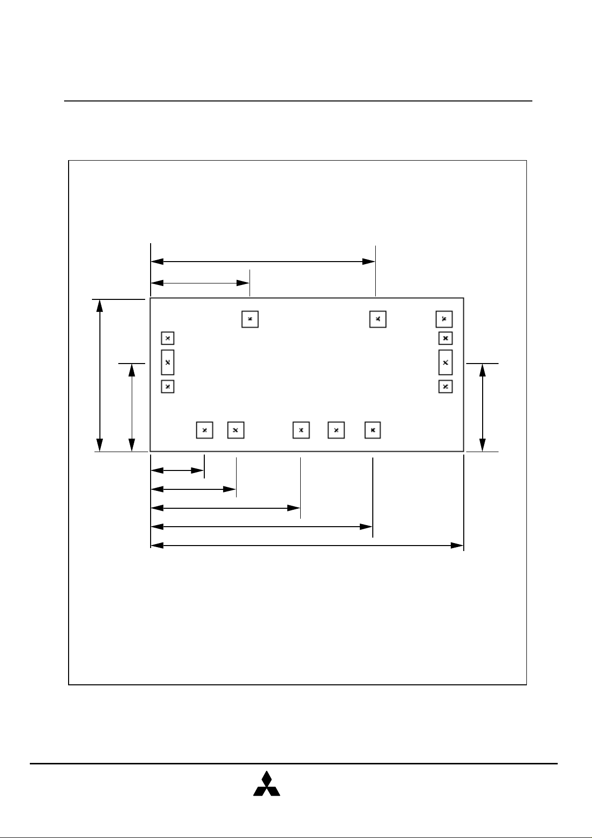
DIE SIZE AND BOND PAD LOCATION(UNIT : µM)
1410
620
950
GND
Vg1 Vg2
MGFC5211
GND
GND
550
RF in
GND
R(Vd1) Vd1
340
530
935
1380
R(Vd2) Vd2
1940
X Dimention 1.94 mm
Y Dimention 0.95 mm
GND
RF out
GND
550
MITSUBISHI
ELECTRIC
as of July '98
Page 3

PRELIMINARY
Notice : This is not a final specification
Some parametric limits are subject to change.
TYPICAL CHARACTERISTICS
Small Signal Performances
(Vd = 5 V, Id1 = 90 mA, Id2 = 180 mA, Ta = 25 ˚C)
20
10
S21
MITSUBISHI SEMICONDUCTOR <GaAs MMIC>
MGFC5211
K-Band 2-Stage Power Amplifier
0
-10
-20
-30
10 15 20 25 30
Frequency [GHz]
Output Power Performances
(Vd = 5 V, Id1 = 90 mA, Id2 = 180 mA, Ta = 25 ˚C)
30
f = 22.4 GHz
25
20
S11
S22
50
40
30
15
10
5
-10 -5 0 5 10 15 20
Pin [dBm]
MITSUBISHI
ELECTRIC
20
10
0
as of July '98
Page 4

PRELIMINARY
Notice : This is not a final specification
Some parametric limits are subject to change.
AN EXAMPLE OF TEST CIRCUIT
Vg1 Vg2
MITSUBISHI SEMICONDUCTOR <GaAs MMIC>
MGFC5211
K-Band 2-Stage Power Amplifier
Cb Cb
Vg1 Vg2
RFin RFout
R(Vd1)
Vd1 Vd2GND
R(Vd2)
CbCb
Vd1 Vd2
: Chip Condenser ( 39 pF )
Cb > 100 µF
MITSUBISHI
ELECTRIC
as of July '98
 Loading...