

Page 1
MITSUBISHI SEMICONDUCTOR <GaAs MMIC>
MGF7169C
Technical Note
Specifications are subject to change without notice.
DESCRIPTION
The MGF7169C is a monolithic microwave integrated
circuit for use in CDMA base handheld phone.
FEATURES
Low voltage operation :
Vd=3.0V
High output power :
Po=28dBm typ. @f=1.85~1.91GHz
Low distortion :
ACP=-46dBc max. @Po=28dBm
High efficiency :
Id=520mA typ. @Po=28dBm
Small size :
7.0 x 6.1 x 1.1 mm
Surface mount package
2 Stage Amplifier
External matching circuit is required
APPLICATION
1.9GHz band handheld phone
UHF BAND GaAs POWER AMPLIFIER
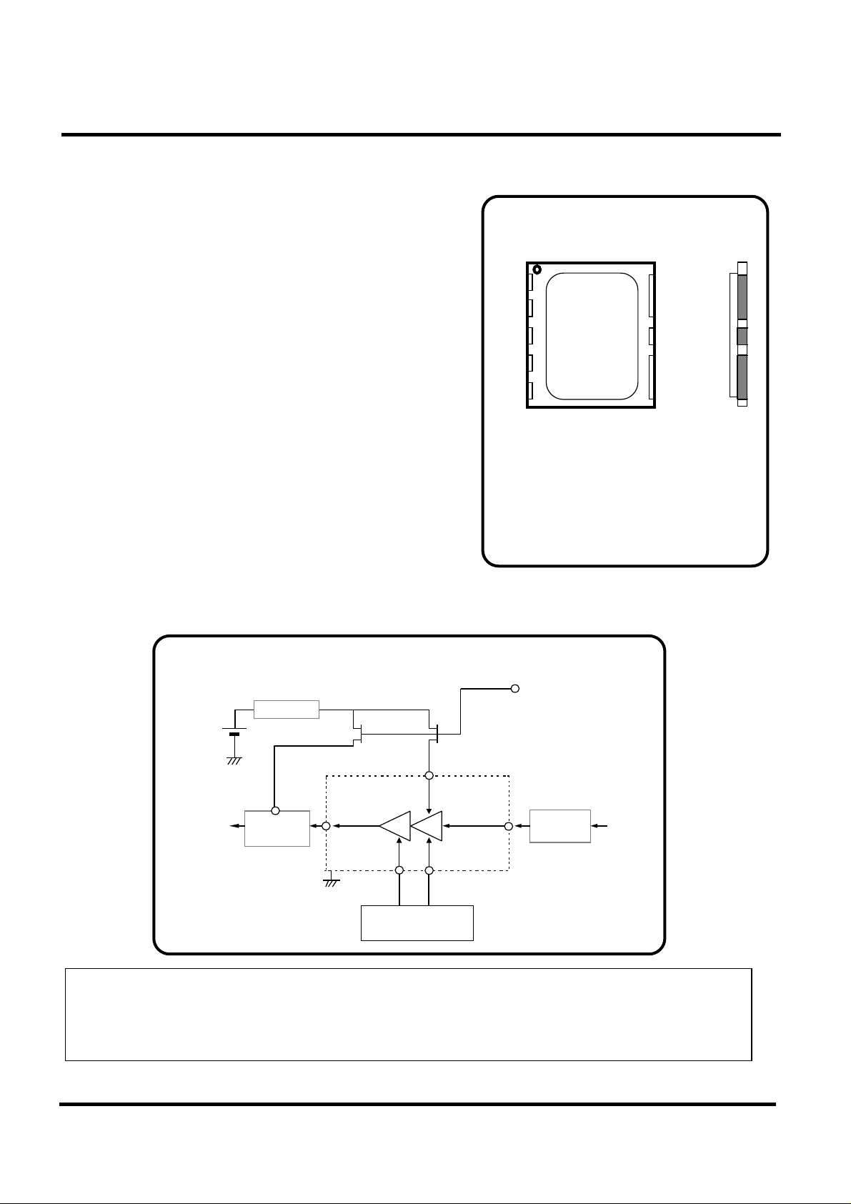
PIN CONFIGURATION
(TOP VIEW)
Pi
Vg1
Vd1
MC
Vg2
: RF input
Pi
: RF output
Po
: Drain bias 1
Vd1
: Drain bias 2
Vd2
: Gate bias
Vg
: Note1
MC
: Connect to GND
GND
: Connect to GND
CASE
GND
GND
Vd2 / Po
QUALITY GRADE
Note1:Connect to matching circuit
GG
Block Diagram of this IC and Application Circuit Example.
VDD
Regulator
Battery
VD1
VD2
Pout
*Mitsubishi Electric Corporation puts the maximum effort into making semiconductor products better and reliable, but there
is always the possibility that trouble may occur with them. Trouble with semiconductors may lead to personal injury, fire or
property damage. Remember to give due consideration to safety when making your circuit designs, with appropriate
measures such as (i) placement of substitutive, auxiliary, circuits, (ii) use of non-flammable material or (iii) prevention
against any malfunction or mishap.
Matching
circuit
MGF7169C
HPA
VG1 VG2
Negative voltage
generator
Matching
circuit
Pin
MITSUBISHI ELECTRIC
(1/20)
Aug. '97
Page 2
MITSUBISHI SEMICONDUCTOR <GaAs MMIC>
Preliminary
information
ABSOLUTE MAXIMUM RATINGS (Ta=25˚C)
Symbol Parameter Ratings Unit
Vd1,Vd2
Vg
Pi
Tc(op)
Tstg
*1.Each maximum rating is guaranteed independently.
Drain supply voltage
Gate supply voltage
Input power dBm15
Operating case temperature
Storage temperature
ELECTRICAL CHARACTERISTICS (Ta=25˚C)
Symbol
Parameter
6 V
-4 V
-30 ~ +85
-30 ~ +100
Test conditions
MGF7169C
UHF BAND GaAs POWER AMPLIFIER
˚C
˚C
Limits
MIN TYP MAX
Unit
f
Idt
Idle_Id Idle current
Pout
Ig Gate current
rin input VSWR
—
—
frequency
Total drain current
Output power
Damage
with-standing
Stability
Note
Note
ACP<-42dBc (1.25MHz off-set.) Vd1=Vd2=3.0V
ACP<-44dBc (1.25MHz off-set.) Vd1=Vd2=3.0V
ACP<-46dBc (1.25MHz off-set.) Vd1=Vd2=3.0V
ACP<-44dBc (1.25MHz off-set.) Vd1=Vd2=3.3V
Vg1=Vg2=-2.0V, Po=28dBm
Vg1=Vg2=-2.5V, Po=12dBm
Vd1=Vd2=3.0V,Vg1=Vg2=-2.0V,
Pin=7dBm CDMA modulated signal
based on IS-95 STD.
(1.2288Mbps spreading,OQPSK)
Vd1=Vd2=3.0V,
Pin=7dBm,
Load VSWR=10, All phase
Time=10 sec
Vd1=Vd2=3.0V,
Pin=7dBm,
Load VSWR=3:1, All phase
1850 1910 MHz
— —
— —
—
— —
—
— —
— —
— —
No oscillation
Spurious level≤-60dBc
—
450
480
520
450
150
50
28
No damage
—
——
——
—
3
mA
mA
dBm
mA-3
dBc-302sp 2nd harmonics
—
*CDMA is code division multiple Access. OQPSK is modulation method, off-set quadrature phase shift keying.
Electrical characteristics are changed by the external matching circuit.
Limits are guaranteed by using MITSUBISHI test fixture.
Note : Sampling inspection
MITSUBISHI ELECTRIC
(2/20)
Aug. '97
Page 3
MITSUBISHI SEMICONDUCTOR <GaAs MMIC>
Preliminary
information
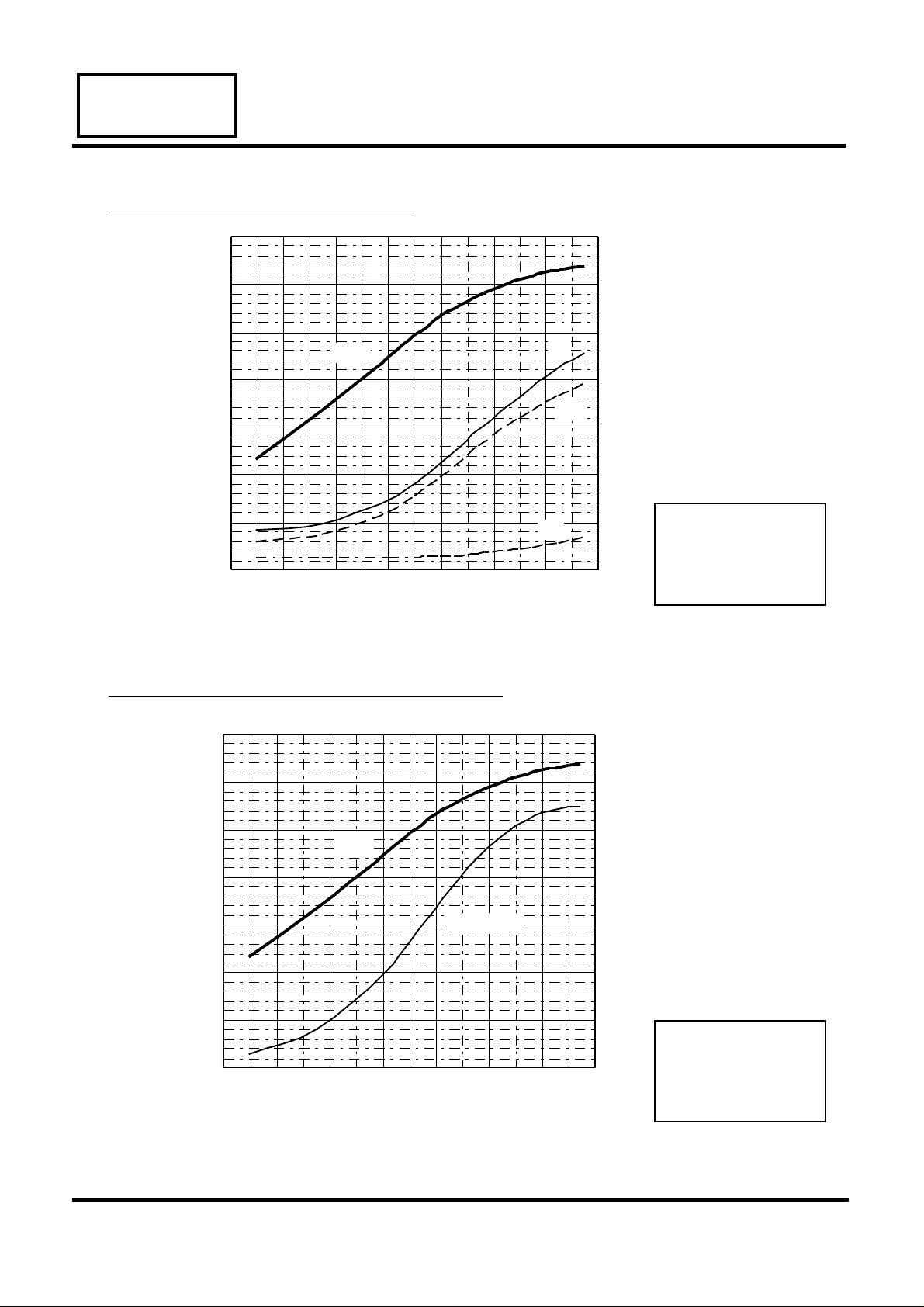
Pin vs. Pout,Id for CDMA
35
30
25
Pout
20
15
Pout (dBm)
10
5
0
-12 -8 -4 0 4 8 12 16
MGF7169C
UHF BAND GaAs POWER AMPLIFIER
1400
1200
1000
Idt
800
Id2
Id1
600
400
200
0
Id (mA)
Fin=1880MHz
Vd1=Vd2=3.0V
Vg1=Vg2=-2.0V
CDMA evaluation
Pin (dBm)
Pin vs. Pout,Efficiency for CDMA
35
30
25
20
15
Pout (dBm)
10
5
0
-12 -8 -4 0 4 8 12 16
Pout
Efficiency
Pin (dBm)
70
60
50
40
30
Efficiency (%)
20
10
0
Fin=1880MHz
Vd1=Vd2=3.0V
Vg1=Vg2=-2.0V
CDMA evaluation
MITSUBISHI ELECTRIC
(3/20)
Aug. '97
Page 4
MITSUBISHI SEMICONDUCTOR <GaAs MMIC>
Preliminary
information
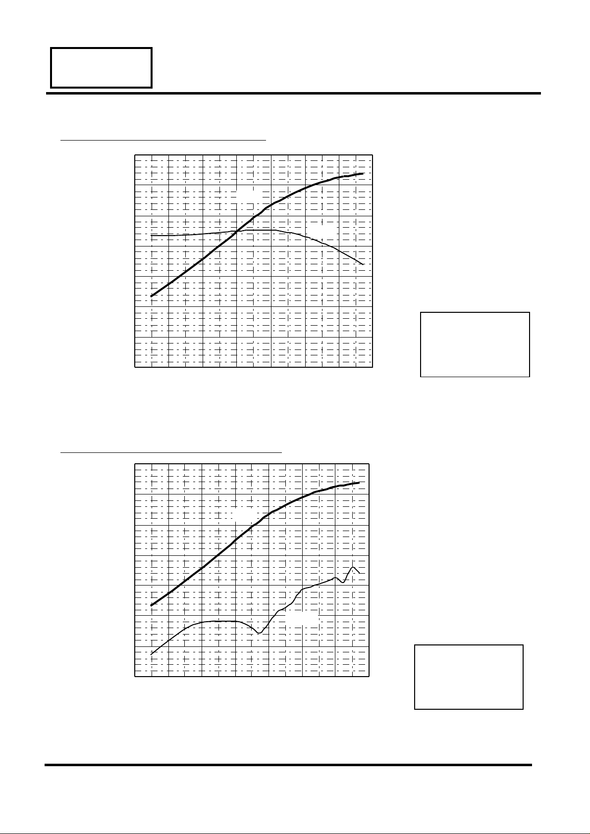
Pin vs.Pout,Gain for CDMA
35
30
Pout
25
20
15
Pout (dBm)
10
5
0
-12 -8 -4 0 4 8 12 16
MGF7169C
UHF BAND GaAs POWER AMPLIFIER
35
30
25
Gain
20
15
GAIN (dB)
10
Fin=1880MHz
5
0
Vd1=Vd2=3.0V
Vg1=Vg2=-2.0V
CDMA evaluation
Pin (dBm)
Pin vs. Pout,ACPR for CDMA
35
30
Pout
25
20
15
Pout (dBm)
10
5
0
-12 -8 -4 0 4 8 12 16
Pin (dBm)
ACPR
15
5
-5
-15
-25
-35
-45
-55
ACPR (dBc)
Fin=1880MHz
Vd1=Vd2=3.0V
Vg1=Vg2=-2.0V
CDMA evaluation
MITSUBISHI ELECTRIC
(4/20)
Aug '97
Page 5
MITSUBISHI SEMICONDUCTOR <GaAs MMIC>
Preliminary
information
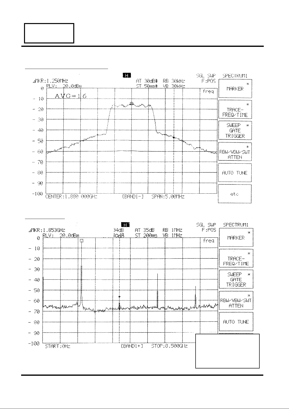
Spectral Plot of CDMA
ACPR=-32.31dBc
MGF7169C
UHF BAND GaAs POWER AMPLIFIER
Harmonics
2SP=-53.3dBc
3SP=-31.3dBc
Fin=1880MHz
Vd1=Vd2=3.0V
Vg1=Vg2=-2.0V
Pout=28dBm
CDMA evaluation
MITSUBISHI ELECTRIC
(5/20)
Aug. '97
Page 6
MITSUBISHI SEMICONDUCTOR <GaAs MMIC>
Preliminary
information
Vd dependence of Pin vs.Pout,Idt
35
30
25
20
15
Pout (dBm)
10
5
0
-12 -8 -4 0 4 8 12 16
Pout
Idt
MGF7169C
UHF BAND GaAs POWER AMPLIFIER
1400
1200
1000
800
600
400
200
0
Id (mA)
Fin=1880MHz
Vg1=Vg2=-2.0V
CDMA evaluation
Vd=2.6V
Vd=3.0V
Vd=3.4V
Pin (dBm)
Vd dependence of Pin vs.Pout,Efficiency
35
30
25
20
15
Pout (dBm)
10
5
0
-12 -8 -4 0 4 8 12 16
Pout
Efficiency
70
60
50
40
30
Efficiency (%)
20
10
0
Vd=2.6V
Vd=3.0V
Vd=3.4V
Fin=1880MHz
Vg1=Vg2=-2.0V
CDMA evaluation
Pin (dBm)
MITSUBISHI ELECTRIC
(6/20)
Aug. '97
Page 7

MITSUBISHI SEMICONDUCTOR <GaAs MMIC>
Preliminary
information
Vd dependence of Pin vs.Pout,Gain
35
30
25
20
15
Pout (dBm)
10
5
0
-12 -8 -4 0 4 8 12 16
Pout
Gain
MGF7169C
UHF BAND GaAs POWER AMPLIFIER
35
30
25
20
15
10
5
0
GAIN (dB)
Fin=1880MHz
Vg1=Vg2=-2.0V
CDMA evaluation
Vd=2.6V
Vd=3.0V
Vd=3.4V
Pin (dBm)
Vd dependence of Pin vs.Pout,ACPR
35
30
Pout
25
20
15
Pout (dBm)
10
5
0
-12 -8 -4 0 4 8 12 16
ACPR
15
5
-5
-15
-25
-35
-45
-55
ACPR (dBc)
Fin=1880MHz
Vg1=Vg2=-2.0V
CDMA evaluation
Vd=2.6V
Vd=3.0V
Vd=3.4V
Pin (dBm)
MITSUBISHI ELECTRIC
Aug. '97
(7/20)
Page 8

MITSUBISHI SEMICONDUCTOR <GaAs MMIC>
Preliminary
information
Vd dependence of Fin vs. Gain,Idt
30
Idt
25
Gain (dB)
20
15
1.84 1.86 1.88 1.90 1.92
Gain
MGF7169C
UHF BAND GaAs POWER AMPLIFIER
600
400
Vd=2.6V
Vd=3.0V
Vd=3.4V
200
0
Idt (mA)
Fin=1880MHz
Vg1=Vg2=-2.0V
CDMA evaluation
Frequency (GHz)
Vd dependence of Fin vs. Id1,Id2
150
Id2
100
Id1 (mA)
50
0
1.84 1.86 1.88 1.90 1.92
Id1
Frequency (GHz)
600
400
200
0
Id2 (mA)
Vd=2.6V
Vd=3.0V
Vd=3.4V
Fin=1880MHz
Vg1=Vg2=-2.0V
CDMA evaluation
MITSUBISHI ELECTRIC
(8/20)
Aug. '97
Page 9

MITSUBISHI SEMICONDUCTOR <GaAs MMIC>
Preliminary
information
UHF BAND GaAs POWER AMPLIFIER
Vd dependence of Fin vs. Gain,Efficiency
35
Efficiency
30
Gain (dB)
25
20
1.84 1.86 1.88 1.90 1.92
Gain
50
40
30
Efficiency (%)
20
MGF7169C
Vd=2.6V
Vd=3.0V
Vd=3.4V
Fin=1880MHz
Vg1=Vg2=-2.0V
CDMA evaluation
Frequency (GHz)
Vd dependence of Fin vs. Gain,ACPR
25
20
Gain (dB)
15
10
1.84 1.86 1.88 1.90 1.92
Gain
ACPR
Frequency (GHz)
-10
-20
-30
-40
ACPR (dBc)
Fin=1880MHz
Vg1=Vg2=-2.0V
CDMA evaluation
Vd=2.6V
Vd=3.0V
Vd=3.4V
MITSUBISHI ELECTRIC
(9/20)
Aug. '97
Page 10

MITSUBISHI SEMICONDUCTOR <GaAs MMIC>
Preliminary
information
UHF BAND GaAs POWER AMPLIFIER
Temp. dependence of Fin vs. Gain,ACPR
25
Gain
20
Gain (dB)
15
ACPR
10
-10
-20
-30
-40
MGF7169C
f=1.85GHz
f=1.88GHz
f=1.91GHz
ACPR+1.25MHz (dBc)
Vd1=Vd2=3.0V
Vg1=Vg2=-2.0V
Pout=28dBm
-30 -10 10 30 50 70 90
Temperature (Åé)
Temp. dependence of Fin vs. Id1,Id2
150
Id2
100
Id1 (mA)
50
0
-30 -10 10 30 50 70 90
Id1
600
500
400
300
200
100
0
Id2 (mA)
Vd1=Vd2=3.0V
Vg1=Vg2=-2.0V
Pout=28dBm
f=1.85GHz
f=1.88GHz
f=1.91GHz
Temperature (Åé)
MITSUBISHI ELECTRIC
Aug. '97
(10/20)
Page 11

MITSUBISHI SEMICONDUCTOR <GaAs MMIC>
Preliminary
information
UHF BAND GaAs POWER AMPLIFIER
MGF7169C
Equivalent Circuit of Test Board for CDMA(1.85-1.91GHz)
l=2.0
w=1.0
MGF
7169C
Vd2
1000pF
Pin
l=8.0
w=1.0
l=8.5
w=1.0
2.5pF
1.5pF
l=23.5
w=0.5
l=2.0
w=2.2
4.0pF
4.5pF
Pout
l=11.0
w=1.0
Unit:mm
SUB. data
Er=4.8
H=600 mm
Metal T=43 mm
MITSUBISHI ELECTRIC
(11/20)
Aug. '97
Page 12

MITSUBISHI SEMICONDUCTOR <GaAs MMIC>
Preliminary
information
UHF BAND GaAs POWER AMPLIFIER
Test Circuit Board for CDMA(1.85-1.91GHz)
2.5pF
1.5pF
Pin
MGF7169C
Vg1
1000pF
10Ohm
1000pF
Vd1
1000pF
Vg2
4.0pF
Pout
4.5pF
3K Ohm (This will be included in PKG for Mass Production)
1000pF
1000pF
Vd2
40 x 60 mm
MITSUBISHI ELECTRIC
(12/20)
SUB. data
ER=4.8
H=600µm
Metal T=43µm
Aug. '97
Page 13

MITSUBISHI SEMICONDUCTOR <GaAs MMIC>
Preliminary
information
VG1 VG2
Pin Pout
FET1
Matching
circuits
UHF BAND GaAs POWER AMPLIFIER
FET2
MGF7169C
VD1 VD2
ZI(ES)
ZL(ES)
Equivalent circuit of MGF7169C with our test board
: MGF7169C(Ceramic package)
: our test board(Er=4.8, t=0.6mm)
MITSUBISHI ELECTRIC
(13/20)
Aug. '97
Page 14

MITSUBISHI SEMICONDUCTOR <GaAs MMIC>
Preliminary
information
UHF BAND GaAs POWER AMPLIFIER
Input/Output Impedance (@1.85-1.91GHz)
ZI(ES) = 6.8 - j22.7 (Ω) f=1.85GHz
6.7 - j21.3 (Ω) f=1.88GHz
6.6 - j19.8 (Ω) f=1.91GHz
ZL(ES) = 4.3 - j3.2 (Ω) f=1.85GHz
4.2 - j2.7 (Ω) f=1.88GHz
4.0 - j2.3 (Ω) f=1.91GHz
ZL(ES) on SMITH CHART
MGF7169C
1.91GHz
X
X
X
1.88GHz
1.85GHz
Conditions;
Vd1=Vd2=3.0V
Vg1=Vg2=-2.0V
Pout=28dBm
MITSUBISHI ELECTRIC
(14/20)
Aug. '97
Page 15

MITSUBISHI SEMICONDUCTOR <GaAs MMIC>
Preliminary
information
OUTLINE DRAWING
6.1+/-0.2
Note1
1
2
3
7.0+/-0.2
4
5
5.2
Unit : mm
MGF7169C
UHF BAND GaAs POWER AMPLIFIER
0.3
8
7
6
6.2
1.1+/-0.2
8 - (0.5)
P1.27 x 4 = 5.08+/-0.1
2 - (2.4)
8 - (0.4)
4 - R0.2
(1.2)2 - (0.1)
4.28
2 - 2.06
0.3
Terminal Connection
RF IN (Pi)
1
Vg1
2
3
Vd1
4
MC
5
Vg2
6
RF OUT (Po) & Vd2
7
GND
8
GND
6 - 0.8+/-0.1
2 - (0.1)
4.1
8 - (4.9)
Note1 : 1 pin mark
Note2 : The values without tolerance are typical.
MITSUBISHI ELECTRIC
(15/20)
Case:GND
Aug. '97
Page 16

MITSUBISHI SEMICONDUCTOR <GaAs MMIC>
Preliminary
information
Recommended Mount Pad
MGF7169C
UHF BAND GaAs POWER AMPLIFIER
2.50
1.0
0.45
7.40
1.2
1.27 x 4=5.08
0.9
0.8
4.10
4.90
2.14
1.4
2.16
0.8
Unit:mm
MITSUBISHI ELECTRIC
(16/20)
Aug. '97
Page 17

MITSUBISHI SEMICONDUCTOR <GaAs MMIC>
Preliminary
information
Recommended Temperature Profile
1) Infrared Reflow and Air Reflow Temperature Profile
max. 10sec
1~4 deg.C/sec
Temperature
MGF7169C
UHF BAND GaAs POWER AMPLIFIER
max. 240 deg.C
1~4 deg.C/sec
150 deg.C
Approx. 60sec
Time
Notes 1) Temperature profile on package surface
2) Reflow process : Up to three times
MITSUBISHI ELECTRIC
(17/20)
Aug. '97
Page 18

MITSUBISHI SEMICONDUCTOR <GaAs MMIC>
Preliminary
information
UHF BAND GaAs POWER AMPLIFIER
MGF7169C
Lumped Elements
Equivalent Circuit of Test Board for CDMA(1.85-1.91GHz)
Vd2
Chip Inductor
10nH
1000pF
Pin
A
1.5pF
l=2.0
w=1.0
1.0pF
l=2.0
w=2.2
MGF
7169C
B
F
D
Pout
15pF
4.0pF
C
Unit:mm
SUB. data
Er=4.8
H=600 um
Metal T=43 um
MITSUBISHI ELECTRIC
(18/20)
Oct. '97
Page 19

MITSUBISHI SEMICONDUCTOR <GaAs MMIC>
Preliminary
information
UHF BAND GaAs POWER AMPLIFIER
Lumped Elements
Test Circuit Board for CDMA(1.85-1.91GHz)
A
1.0pF
B
Pin
1.5pF
MGF7169C
5mm
1000pF
1000pF
10Ohm
1000pF
1000pF
Vg1
Line
Chip Capacitor
Chip Inductor
This device needs 4 chip capacitors,1 chip inductor
and 2 transmission lines to make input and output
matching circuit.
Vd1
3K Ohm (This will be included in PKG for Mass Production)
Vg2
C
4.0pF
10nH
F
15pF
1000pF
40 x 60 mm
D
Pout
Vd2
SUB. data
ER=4.8
H=600um
Metal T=43um
MITSUBISHI ELECTRIC
(19/20)
Oct. '97
Page 20

MITSUBISHI SEMICONDUCTOR <GaAs MMIC>
Preliminary
information
Pin
VG1 VG2
FET1
Matching
circuits
MGF7169C
UHF BAND GaAs POWER AMPLIFIER
Pout
FET2
VD1 VD2
ZI(ES)
ZL(ES)
Lumped Elements
Equivalent circuit of MGF7169C with our test board
: MGF7169C(Ceramic package)
: our test board(Er=4.8, t=0.6mm)
MITSUBISHI ELECTRIC
(20/20)
Oct. '97
 Loading...