

Page 1

MGC3130
Single-Zone 3D Tracking and Gesture Controller Data Sheet
Introduction:
The MGC3130 is a three-dimensional (3D) gesture
recognition and tracking controller chip based on
Microchip’s patented GestIC
user command input with natural hand and finger
movements. Utilizing the principles of electrical nearfield sensing, the MGC3130 contains all the building
blocks to develop robust 3D input sensing systems.
Implemented as a low-power mixed-signal
configurable controller, it provides a large set of smart
functional features with integrated signal driver, a
frequency adaptive input path for automatic noise
suppression and a digital signal processing unit.
Microchip’s on-chip Colibri Suite minimizes processing
needs, reduces system power consumption and results
in low software development efforts for fast time-tomarket success. The MGC3130 is a unique solution
that provides gesture information as well as positional
data of the human hand in real time and allows
realization of a new generation of user interfaces
across various industries.
®
technology. It enables
Applications:
• Displays
• Notebooks/Keyboards/PC Peripherals
• Mobile Phones
• Tablet Computers
• Electronic Readers
• Remote Controls
• Game Controllers
Power Features:
• Variety of Several Power Operation modes
include:
- Processing mode: 20 mA @ 3.3V, typical
- Programmable Self Wake-up: 110 µA @ 3.3V
- Deep Sleep: 9 µA @ 3.3V, typical
Key Features:
• Recognition of 3D Hand Gestures and x, y, z
Positional Data
• Proximity and Touch Sensing Capabilities
• Built-in Colibri Gesture Suite
• Advanced 3D Signal Processing Unit
• Detection Range: 0 to 15 cm
• Receiver Sensitivity: <1 fF
• Position Rate: 200 positions/sec
• Spatial Resolution: up to 150 dpi
• Carrier Frequency: 44 kHz to 115 kHz
• Channels Supported:
- Five receive (Rx) channels
- One transmit (Tx) channel
• On-chip Auto Calibration
• Low Noise Radiation due to Low Transmit Voltage
and Slew Rate Control
• Noise Susceptibility Reduction:
- On-chip analog filtering
- On-chip digital filtering
- Automatic frequency hopping
• Enables the use of Low-Cost Electrode Material
including:
- Printed circuit board
- Conductive paint
- Conductive foil
- Laser Direct Structuring (LDS)
- Touch panel ITO structures
• Field Upgrade Capability
• Small Outline, 28-lead QFN package, 5x5 mm
• Operating Voltage: 2.5V to 3.465V (single supply)
• Temperature Range: -20°C to +85°C
Peripheral Features:
•2x I2C™ or SPI Interface for Configuration and
Streamin g of Positional and Gesture Data
• Multi-zone Support via Master/Slave Architecture
2012-2013 Microchip Technology Inc. Advance Information DS40001667C-page 1
Page 2

MGC3130
QFN
1
2
3
4
5
6
715
8
9
10
11
12
13
14
16
17
18
19
20
21
26
25
24
23
22
28
27
VCAPS
VINDS
VSS2
RX0
RX1
RX2
RX3
RX4
V
CAPA
VSS3
VCAPD
EIO0
EIO1
EIO2
EIO5/SI1
EIO4/SI0
EIO3
NC
NC
NC
IS2
EIO6/SI2
MCLR
T
XD
NC
V
SS1
VDD
EIO7/SI3
MGC3130
EXP-29
Package Type
The device is available in 28-lead QFN packaging (see
Figure 1).
FIGURE 1: 28-PIN DIAGRAM (MGC3130)
DS40001667C-page 2 Advance Information 2012-2013 Microchip Technology Inc.
Page 3

MGC3130
TABLE 1: 28-PIN QFN PINOUT DESCRIPTION
Pin Name
VCAPS 1P— External filter capacitor (10 µF) connection for internal STEP-UP
V
INDS 2P
SS2 3P
V
RX0 4 I Analog
RX1 5 I Analog
RX2 6 I Analog
RX3 7 I Analog
RX4 8 I Analog
CAPA 9P
V
SS3 10 P
V
CAPD 11 P
V
EIO0 12 I/O ST Extended IO0 (EIO0)/Transfer Status (TS). TS line requires
EIO1 13 I/O ST Extended IO1 (EIO1)/Interface Selection Pin 1 (IS1).
EIO2 14 I/O ST Extended IO2 (EIO2)/IRQ0.
IS2 15 I ST Interface Selection Pin 2 (IS2).
NC 16
NC 17
NC 18
EIO3 19 I/O ST Extended IO3 (EIO3)/IRQ1/SYNC.
EIO4/SI0 20 I/O ST Extended IO4 (EIO4)/Serial Interface 0 (SI0): I2C™_SDA0/
EIO5/SI1 21 I/O ST Extended IO5 (EIO5)/Serial Interface 1 (SI1): I
EIO6/SI2 22 I/O ST Extended IO6 (EIO6)/Serial Interface 2 (SI2): I
EIO7/SI3 23 I/O ST Extended IO7 (EIO7)/Serial Interface 3 (SI3): I
MCLR
T
XD 25 O Analog Transmit electrode connection.
NC 26
SS1 27 P
V
VDD 28 P
EXP 29 P
Legend: P = Power; ST = Schmitt Trigger input with CMOS levels; O = Output; I = Input; — = N/A
Pin
Number
Pin Type Buffer Type Description
converter (optional).
—
External inductor (4.7 µH) + Schottky diode connection for internal
STEP-UP converter usage (optional).
—
Ground reference for the STEP-UP converter.
Analog input channels: Receive electrode connection.
—
External filter capacitor (4.7 µF) connection for internal analog
voltage regulator (3V).
—
—
Common ground reference for analog and digital domain.
External filter capacitor (4.7 µF) connection for internal digital
voltage regulator (1.8V).
external 10 kpull-up
——
——
——
Reserved: do not connect.
Reserved: do not connect.
Reserved: do not connect.
SPI_MISO. When I
2
C™ is used, this line requires an external 1.8
kpull-up.
2
C™_SCL0/SPI_-
MOSI. When I
2
C™ is used, this line requires an external 1.8 k
pull-up.
2
C™_SDA1/
SPI_CS. When I
2
C™ is used, this line requires an external 1.8 k
pull-up.
2
C™_SCL1/SPI_S-
CLK. When I
2
C™ is used, this line requires an external 1.8 k
pull-up.
24 I/P ST Master Clear (Reset) input. This pin is an active-low Reset to the
device. It requires external 10 kpull-up.
——
—
—
Reserved: do not connect.
Common ground reference for analog and digital domains.
Positive supply for peripheral logic and I/O pins.
It requires an external filtering capacitor (100 nF).
—
Exposed pad. It should be connected to Ground.
2012-2013 Microchip Technology Inc. Advance Information DS40001667C-page 3
Page 4

MGC3130
Table of Contents
1.0 Theory of Operation: Electrical Near-Field (E-Field Sensing).................................................................................................... 5
2.0 Feature Description.................................................................................................................................................................... 7
3.0 System Architecture ................................................................................................................................................................ 10
4.0 Functional Description ............................................................................................................................................................. 13
5.0 Application Architecture ........................................................................................................................................................... 23
6.0 Interface Description ................................................................................................................................................................ 24
7.0 Hardware Integration ............................................................................................................................................................... 33
8.0 Development Support .............................................................................................................................................................. 36
9.0 Electrical Specifications ........................................................................................................................................................... 37
10.0 Packaging Information ............................................................................................................................................................. 38
The Microchip Web Site....................................................................................................................................................................... 43
Customer Change Notification Service ................................................................................................................................................ 43
Customer Support ................................................................................................................................................................................ 43
Product Identification System .............................................................................................................................................................. 44
TO OUR VALUED CUSTOMERS
It is our intention to provide our valued customers with the best documentation possible to ensure successful use of your Microchip
products. To this end, we will continue to improve our publications to better suit your needs. Our publications will be refined and
enhanced as new volumes and updates are introduced.
If you have any questions or comments regarding this publication, please contact the Marketing Communications Department via
E-mail at docerrors@microchip.com or fax the Reader Response Form in the back of this data sheet to (480) 792-4150. We
welcome your feedback.
Most Current Data Sheet
To obtain the most up-to-date version of this data sheet, please register at our Worldwide Web site at:
http://www.microchip.com
You can determine the version of a data sheet by examining its literature number found on the bottom outside corner of any page.
The last character of the literature number is the version number, (e.g., DS30000A is version A of document DS30000).
Errata
An errata sheet, describing minor operational differences from the data sheet and recommended workarounds, may exist for current
devices. As device/documentation issues become known to us, we will publish an errata sheet. The errata will specify the revision
of silicon and revision of document to which it applies.
To determine if an errata sheet exists for a particular device, please check with one of the following:
• Microchip’s Worldwide Web site; http://www.microchip.com
• Your local Microchip sales office (see last page)
When contacting a sales office, please specify which device, revision of silicon and data sheet (include literature number) you are
using.
Customer Notification System
Register on our web site at www.microchip.com to receive the most current information on all of our products.
DS40001667C-page 4 Advance Information 2012-2013 Microchip Technology Inc.
Page 5

MGC3130
1.0 THEORY OF OPERATION: ELECTRICAL NEAR-FIELD (E-FIELD) SENSING
Microchip’s GestIC is a 3D sensor technology which
utilizes an electric field (E-field) for advanced proximity
sensing. It allows realization of new user interface
applications by detection, tracking and classification of
a user’s hand or finger motion in free space.
E-fields are generated by electrical charges and
propagate three-dimensionally around the surface,
carrying the electrical charge.
Applying direct voltages (DC) to an electrode results in
a constant electric field. Applying alternating voltages
(AC) makes the charges vary over time and thus, the
field. When the charge varies sinusoidal with frequency
f, the resulting electromagnetic wave is characterized
by wavelength λ = c/f, where c is the wave propagation
velocity — in vacuum, the speed of light. In cases
where the wavelength is much larger than the electrode
geometry, the magnetic component is practically zero
and no wave propagation takes place. The result is
quasi-static electrical near field that can be used for
sensing conductive objects such as the human body.
Microchip’s GestIC technology uses transmit (Tx)
frequencies in the range of 100 kHz which reflects a
wavelength of about three kilometers. With electrode
geometries of typically less than fourteen by fourteen
centimeters, this wavelength is much larger in
comparison.
In case a person’s hand or finger intrudes the electrical
field, the field becomes distorted. The field lines are
drawn to the hand due to the conductivity of the human
body itself and shunted to ground. The threedimensional electric field decreases locally. Microchip’s
GestIC technology uses a minimum number of four
receiver (Rx) electrodes to detect the E-field variations
at different positions to measure the origin of the
electric field distortion from the varying signals
received. The information is used to calculate the
position, track movements and to classify movement
patterns (gestures).
The simulation results in Figure 1-1 and Figure 1-2
show the influence of an earth-grounded body to the
electric field. The proximity of the body causes a compression of the equipotential lines and shifts the Rx
electrode signal levels to a lower potential which can be
measured.
FIGURE 1-1: EQUIPOTENTIAL LINES
OF AN UNDISTORTED
E-FIELD
FIGURE 1-2: EQUIPOTENTIAL LINES
OF A DISTORTED E-FIELD
2012-2013 Microchip Technology Inc. Advance Information DS40001667C-page 5
Page 6

MGC3130
1.1 GestIC Technology Benefits
• GestIC E-field sensors are not impacted by
ambient influences such as light or sound, which
have a negative impact to the majority of other 3D
technologies.
• The GestIC technology has a high immunity to
noise, provides high update rates and resolution,
low latency and is also not affected by clothing,
surface texture or reflectivity.
• A carrier frequency in the range of 44-115 kHz is
being used with the benefit of being outside the
regulated radio frequency range. In the same
manner, GestIC is not affected by radio
interference.
• Usage of thin low-cost materials as electrodes
allow low system cost at slim industrial housing
designs.
• The further use of existing capacitive sensor
structures such as a touch panel’s ITO coating
allow additional cost savings and ease the
integration of the technology.
• Electrodes are invisible to the users’ eye since
they are implemented underneath the housing
surface or integrated into a touch panel’s ITO
structure.
• GestIC works centrically over the full sensing
space. Thus, it provides full surface coverage
without any detection blind spots.
• Only one GestIC transmitter electrode is used for
E-field generations. The benefit is an overall low
power consumption and low radiated EMC noise.
• Since GestIC is basically processing raw
electrode signals and computes them in real time
into pre-processed gestures and accurate x, y, z
positional data, it provides a highly flexible user
interface technology for any kind of electronic
devices.
DS40001667C-page 6 Advance Information 2012-2013 Microchip Technology Inc.
Page 7

MGC3130
Digital Signal Processing
Colibri Suite
Position
Tracking
Gesture
Recognition
Approach
Detection
2.0 FEATURE DESCRIPTION
2.1 Gesture Definition
A hand gesture is the movement of the hand to express
an idea or meaning. The GestIC technology accurately
allows sensing of a user’s free space hand motion for
contact free position tracking, as well as three-dimensional (3D) gesture recognition based on classified
movement patterns.
2.2 GestIC Library
MGC3130 is being provided with a GestIC Library,
stored on the chip’s Flash memory. The library
includes:
• Colibri Suite: Digital Signal Processing (DSP)
algorithms and feature implementations.
• System Control: MGC3130 hardware control
features such as Analog Front End (AFE) access,
interface control and parameters storage.
• Library Loader: GestIC Library update through the
application host’s interface.
2.2.1 COLIBRI SUITE
The Colibri Suite combines data acquisition, digital
signal processing and interpretation.
The Colibri Suite functional features are illustrated in
Figure 2-1 and described in the following sections.
FIGURE 2-1: COLIBRI SUITE CORE
2.2.1.1 Position Tracking
The Colibri Suite’s Position Tracking feature provides
three-dimensional hand position over time and area.
The absolute position data is provided according to the
defined origin of the Cartesian coordinate system (x, y,
z). Position Tracking data is continuously acquired in
parallel to Gesture Recognition. With a position rate of
up to 200 positions/sec., a maximum spatial resolution
of 150 dpi is achieved.
ELEMENTS
2.2.1.2 Gesture Recognition
The Colibri Suite’s gesture recognition model detects
and classifies hand movement patterns performed
inside the sensing area.
Using advanced stochastic classification based on
Hidden Markov Model (HMM), industry best gesture
recognition rate is being achieved. In addition, there
are some gestures derived from the combination of
Gesture Recognition and spatial information.
The Colibri Suite includes a set of predefined hand
gestures which contains flick, circular and symbol
gestures as the ones outlined below:
• Flick gestures
A flick gesture is a unidirectional gesture in a quick
flicking motion. An example may be a hand movement
from West to East within the sensing area, from South
to North, etc.
• Circular gestures
A circular gesture is a round-shaped hand movement
defined by direction (clockwise/counterclockwise)
without any specific start position of the user’s hand.
Two types of circular gestures are distinguished by
GestIC technology:
1. Discrete Circles
Discrete Circles are recognized after performing a
hand movement inside the sensing area. The
recognition result (direction: clockwise/
counterclockwise) is provided after the hand movement
stops or the hand exits the detection area. The Discrete
Circles are typically used as dedicated application
control commands.
2. AirWheel
An AirWheel is the recognition of continuouslyperformed circles inside the sensing area and provides
information about the rotational movement in real time.
It starts after at least one quadrant of a circle is
recognized and provides continuously counter
information which increments/decrements according to
the movement’s direction (clockwise/
counterclockwise). The AirWheel can be adjusted for
convenient usage in various applications (e.g., volume
control, sensitivity adjustment or light dimming).
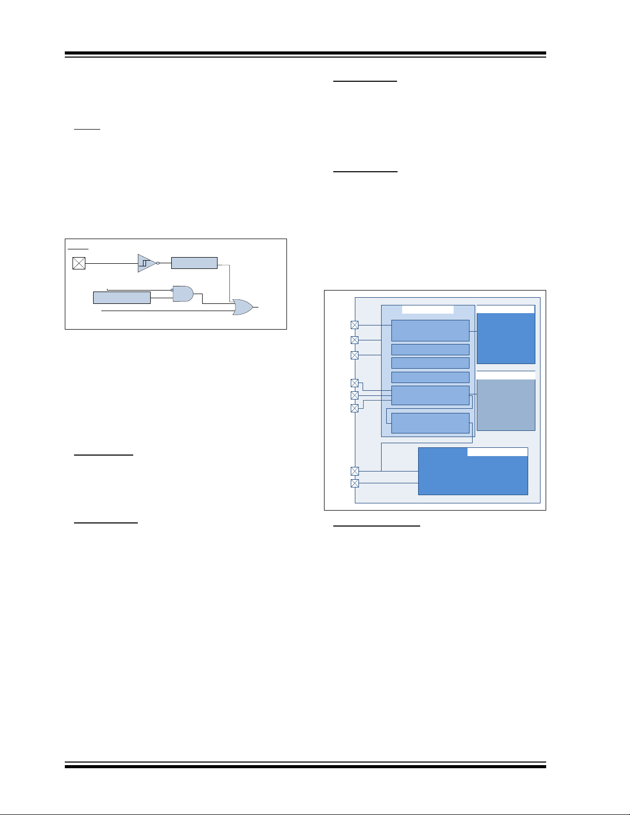
ensor Touch Gestures
•S
A Sensor Touch is a multi-zone gesture that reports up
to five concurrently-performed touches on the system’s
electrodes.
The Sensor Touch provides information about Touch
and Tapping:
1. Touch
The Sensor Touch indicates an event during which a
GestIC electrode is touched. This allows distinction
between short and long touches.
2. Tap and Double Tap
2012-2013 Microchip Technology Inc. Advance Information DS40001667C-page 7
Page 8

MGC3130
Touch
Touch
detected
Tap
Tap
detected
Single Tap Duration
0s-1s
Double Tap
Double Tap
detected
Double Tap Duration
0s-1s
The Tap and Double Tap signalize short taps and
double taps on each system electrode. The Tap length
and Double Tap interval are adjustable.
- Single Tap Delay: A Single Tap is detected
when touching the surface of an electrode
first and after the hand is pulled out of the
touch area. The Single Tap is only detected
when the timing between the touch and the
release of the touch event is smaller than the
adjusted delay. Increasing the time allows the
user more time to perform the tap. The range
for the adjusted delay can be between 0s and
1s.
- Double Tap Delay: The double tap is detected
FIGURE 2-2: SENSOR TOUCH DIAGRAM
when two taps are performed within the
adjusted delay. The range for the adjusted
delay can be between 0s and 1s. The smaller
the selected delay is, the faster the two taps
have to be executed.
• Gesture Port
The Gesture Port enables a flexible mapping of Colibri
Suite feature events to certain output signals at defined
MGC3130’s pins. The individual feature events can be
mapped to one of five EIO Pins and trigger a variety of
signal changes (Permanent high, Permanent low, Toggle, Pulse (5 ms), High Active, Low Active). The Gesture Port simplifies and enhances embedded system
integration.
DS40001667C-page 8 Advance Information 2012-2013 Microchip Technology Inc.
Page 9

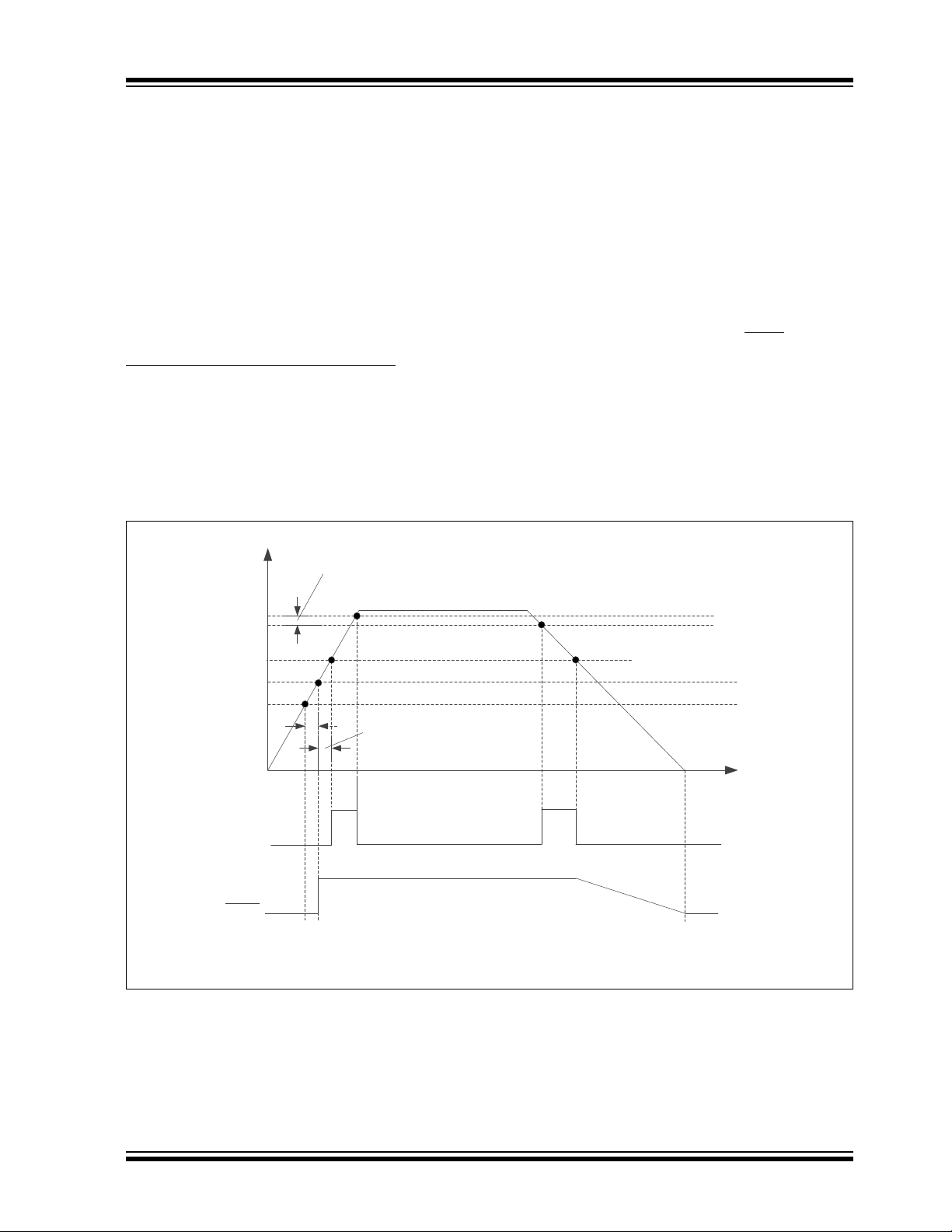
2.2.1.3 Approach Detection
Current
time
Periodic Approach Scans
Calibration
Scan
Periodic Approach Scans
Calibration
Scan
Periodic Approach Scans
Calibration
Scan
Periodic Approach Scans
Scan Interval
20ms-150ms
Calibrati on Start Scan Interv al
2s-10s
I
sleep
= 9µA
I
5CHSCAN
= 20mA
I
5CHSCAN
: Scan Phase with 5 active RX channel s: Calibrat ion Scan
I
sleep
: Sleep Phase
Calibrati on Final Scan Interv al
2s-1024s
Calibrati on Transition Ti me (Non-user act ivity timeout)
2s-255s
Processing
Mode
Idle Timeout
5s-1024s
Self Wake-up mode
Approach Detection is an embedded power-saving
feature of Microchip’s Colibri Suite. It sends MGC3130
to Sleep mode and scans periodically the sensing area
to detect the presence of a human hand.
Utilizing the in-built Self Wake-up mode, Approach
Detection alternates between Sleep and Scan phases.
During the Scan phases, the approach of a human
hand can be detected while very low power is
consumed. For more details, please see
Section 4.2.4.3 “Self Wake-up Mode”.
A detected approach of a user exceeding configured
threshold criteria will alternate the MGC3130 from Self
Wake-up to Processing mode or even the application
host in the overall system.
Within the Approach Detection sequence, the following
scans are performed:
• Approach Scan
during the Scan phase of the MGC3130’s Self
Wake-up mode. Typically, 1 Rx channel is active
but more channels can be activated via GestIC
Library. The time interval (Scan Interval) between
two consecutive Approach Scans is configurable.
For typical applications, the scan cycle is in a
range of 20 ms to 150 ms. During the Approach
Scan, the activated Rx channels are monitored for
signal changes which are caused by, for example,
an approaching human hand and exceeding the
defined threshold. This allows an autonomous
wake-up of the MGC3130 and host applications at
very low-power consumption.
: An Approach Scan is performed
MGC3130
(1)
• Calibration Scan
feature includes the possibility to perform
additional Calibration Scans for the continuous
adaptation of the electrode system to
environmental changes.
A Calibration Scan is performed during the Scan
phase of the MGC3130’s Self Wake-up mode.
Five Rx channels are active to calibrate the
sensor signals. The Calibration Scan is usually
performed in configurable intervals from 2s to
1024s.
To reduce the power consumption, the number of
scans per second can be decreased after a
certain time of non-user activity. Colibri Suite
provides a full user flexibility to configure the
starting Calibration Scans rate (Calibration Start
Scan Interval), non-user activity time-out
(Calibration Transition Time) and the Calibration
Scans rate (Calibration Final Scan Interval) which
will be used afterwards. A typical implementation
uses Calibration Scans every 2s during the first
two minutes, and every 10s afterwards, until an
approach is detected.
Note 1: The Calibration Scan is only needed for
applications using the Position Tracking
feature.
The timing sequence of the Approach Detection feature
is illustrated in Figure 2-3.
: The Approach Detection
FIGURE 2-3: APPROACH DETECTION SEQUENCE
2012-2013 Microchip Technology Inc. Advance Information DS40001667C-page 9
Page 10

MGC3130
MGC3130
Controller
Analog Front End
Communications
Interfaces
GestIC
®
Library
External
Electrodes
Tx
Rx5
Signal Processing
Unit
To application
host
3.0 SYSTEM ARCHITECTURE
The MGC3130 is the first product based on Microchip’s
GestIC technology. It is developed as a mixed-signal
configurable controller. The entire system solution is
composed by three main building blocks (see
Figure 3-1):
• MGC3130 Controller
• GestIC Library
• External Electrodes
3.1 MGC3130 Controller
The MGC3130 features the following main building
blocks:
• Low Noise Analog Front End (AFE)
• Digital Signal Processing Unit (SPU)
• Flexible Communication Interfaces
It provides a transmit signal to generate the E-field,
conditions the analog signals from the receiving
electrodes and processes these data digitally on the
SPU. Data exchange between the MGC3130 and the
host is conducted via the controller’s communication
interface. For details, please refer to Section 4.0
“Functional Description”.
3.2 GestIC Library
The embedded GestIC Library is optimized to ensure
continuous and real-time free-space Position Tracking
and Gesture Recognition concurrently. It is fullyconfigurable and allows required parameterization for
individual application and external electrodes.
3.3 External Electrodes
Electrodes are connected to MGC3130. An electrode
needs to be individually designed for optimal E-field
distribution and detection of E-field variations inflicted
by a user.
FIGURE 3-1: MGC3130 CONTROLLER SYSTEM ARCHITECTURE
DS40001667C-page 10 Advance Information 2012-2013 Microchip Technology Inc.
Page 11

MGC3130
C
RxTx
C
TxG
C
RxG
System ground
Transmitter signal
Electrode signal
C
H
Earth ground
E-field
To MGC3130
V
Tx
System
Ground
e
Rx
e
Tx
V
RxBuf
V
RxBuf
V
Tx
C
RxTx
C
RxTx
C
RxGCH
++
---------------------------------------------- -=
3.3.1 ELECTRODE EQUIVALENT CIRCUIT
The hand Position Tracking and Gesture Recognition
capabilities of a GestIC system depends on the
electrodes design and their material characteristics.
A simplified equivalent circuit model of a generic
GestIC electrode system is illustrated in Figure 3-2.
FIGURE 3-2: ELECTRODES CAPACITIVE EQUIVALENT CIRCUITRY EARTH GROUNDED
•VTX: Tx electrode voltage
•V
•C
•C
•C
•C
•e
•e
The Rx and Tx electrodes in a GestIC electrode system
build a capacitance voltage divider with the
capacitances C
the electrode design. C
capacitance to system ground driven by the Tx signal.
The Rx electrode measures the potential of the
generated E-field. If a conductive object (e.g., a hand)
approaches the Rx electrode, C
capacitance. This minuscule change in the femtofarad
range is detected by the MGC3130 receiver.
The equivalent circuit formula for the earth-grounded
circuitry is described in Equation 3-1.
: MGC3130 Rx input voltage
RXBUf
: Capacitance between receive electrode and
H
hand (earth ground). The user’s hand can always
be considered as earth-grounded due to the
comparable large size of the human body.
: Capacitance between receive and transmit
RXTX
electrodes
: Capacitance of the receive (Rx) electrode
RXG
to system ground + input capacitance of the
MGC3130 receiver circuit
: Capacitance of the transmit (Tx) electrode
TxG
to system ground
: Rx electrode
Rx
: Tx electrode
Tx
RxTx
and C
which are determined by
RxG
represents the Tx electrode
TxG
changes its
H
EQUATION 3-1: ELECTRODES
EQUIVALENT CIRCUIT
A common example of an earth-grounded device is a
notebook, even with no ground connection via power
supply or ethernet connection. Due to its larger form
factor, it presents a high earth-ground capacitance in
the range of 50 pF and thus, it can be assumed as an
earth-grounded GestIC system.
A brief overview of the typical values of the electrodes
capacitances is summarized in Tab le 3- 1.
TABLE 3-1: ELECTRODES
CAPACITANCES TYPICAL
VALUES
Capacity Typical Value
C
RXTX
C
TXG
C
RXG
C
H
10...30 pF
10...1000 pF
10...30 pF
<1 pF
2012-2013 Microchip Technology Inc. Advance Information DS40001667C-page 11
Page 12

MGC3130
South
West
East
Center
North
Top Layer (Lateral Rx)
Top Layer (Center Rx)
Tx Layer
Note: Ideal designs have low C
ensure higher sensitivity of the electrode
system. Optimal results are achieved with
C
RxTx
range.
and C
values being in the same
RxG
RxTx
and C
RxG
to
3.3.2 STANDARD ELECTRODE DESIGN
The MGC3130 electrode system is typically a doublelayer design with a Tx transmit electrode at the bottom
layer to shield against device ground and thus, ensure
high receive sensitivity. Up to five comparably smaller
Rx electrodes are placed above the Tx layer providing
the spatial resolution of the GestIC system. Tx and Rx
FIGURE 3-3: FRAME SHAPE ELECTRODES
are separated by a thin isolating layer. The Rx
electrodes are typically arranged in a frame
configuration as shown in Figure 3-3. The frame
defines the inside sensing area with maximum
dimensions of 14x14 centimeters. An optional fifth
electrode in the center of the frame may be used to
improve the distance measurement and add simple
touch functionality.
The electrodes’ shapes can be designed solid or
structured. In addition to the distance and the material
between the Rx and Tx electrodes, the shape structure
density also controls the capacitance C
the sensitivity of the system.
RXTX
and thus,
DS40001667C-page 12 Advance Information 2012-2013 Microchip Technology Inc.
Page 13

MGC3130
Host
Signal
Processing
Unit (SPU)
Power Management
Unit (PMU)
Internal clockTX Signal Generation
External
Electrodes
Communication
control
I2C
TM
SPI
MGC3130
Controller
Signal
conditioning
ADC
Signal
conditioning
ADC
Signal
conditioning
ADC
Signal
conditioning
ADC
Signal
conditioning
ADC
FLASH
memory
IOs
Reset block
Voltage Reference
(V
REF)
TXD
RX0
RX1
RX2
RX3
RX4
MCLR
SI0
SI1
SI2
SI3
EIO1
EIO2
EIO3
IS2
EIO0
INTERNAL BUS
Low-Power
Wake-up
4.0 FUNCTIONAL DESCRIPTION
Zone Design) or a single MGC3130 and another circuit
with a corresponding interface, such as a touch screen
Microchip Technology’s MGC3130 configurable
controller uses up to five E-field receiving electrodes.
Featuring a Signal Processing Unit (SPU), a wide
range of 3D gesture applications are being preprocessed on the MGC3130, which allows short
development cycles.
Always-on 3D sensing, even for battery-driven mobile
devices, is enabled due to the chip’s low-power design
and variety of programmable power modes. A Self
Wake-up mode triggers interrupts to the application
host reacting to interaction of a user with the device
and supporting the host system in overall power
controller.
GestIC sensing electrodes are driven by a low-voltage
signal with a frequency in the range of 100 kHz, which
allows their electrical conductive structure to be made
of any low-cost material. Even the reuse of existing
conductive structures, such as a display’s ITO coating,
is feasible, making the MGC3130 an overall, very costeffective system solution.
Figure 4-1 provides an overview of the main building
blocks of MGC3130. These blocks will be described in
the following sections.
reduction.
Featuring a programmable 4-pin digital interface, the
MGC3130 matches a multitude of hardware
requirements. Developers have the choice of data
exchange via I
2
C interfaces, developers have the option to set up a
I
2
C or SPI. Since the device provides two
master-slave architecture between two MGC3130
devices to add an additional sensing area (e.g., Two-
FIGURE 4-1: MGC3130 CONTROLLER BLOCK DIAGRAM
2012-2013 Microchip Technology Inc. Advance Information DS40001667C-page 13
Page 14
MGC3130
MCLR
Glitch Filter
Deep sleep
WDTR
Software Reset (SWR)
WDT Time-out
SYSRST
SPU
Digital
Peripherals
Reset Block
Internal Osc.
VDDC Domain
Analog voltage
regulator
Digital voltage
regulator
Flash
Memory
Wake-up logic
WDTR
EIO
VDDM Domain
STEP-UP converter
VCAPS
VSS2
VDD
VSS1
V
CAPA
V
SS3
ADC
Signal Conditioning Blocks
VDDA Domain
VCAPD
VINDS
VDD Domain
4.1 Reset Block
The Reset block combines all Reset sources. It
controls the device system’s Reset signal (SYSRST).
The following is a list of device Reset sources:
•MCLR
• SWR: Software Reset available through GestIC
• WDTR: Watchdog Timer Reset
A simplified block diagram of the Reset block is
illustrated in Figure 4-2.
FIGURE 4-2: SYSTEM RESET BLOCK
: Master Clear Reset pin
Library
DIAGRAM
• V
DDA Domain: This domain is powered by
DDA = 3.0V. It is generated by an embedded low-
V
impedance and fast linear voltage regulator.
During Deep Sleep mode, the analog voltage
regulator is switched off. V
DDA is the internal
analog power supply voltage for the ADCs and
the signal conditioning. An external block
capacitor, C
• V
DDM Domain: This domain is powered by
DDM = 3.3V. VDDM is the internal power supply
V
EFCA, is required on VCAPA pin.
voltage for the internal Flash memory. This power
supply is depending on VDD voltage range. If
DD ≥ 3.3V, the memory is directly powered
V
through the V
DD pin. In case of VDD < 3.3V, the
Flash power supply is generated internally by an
embedded STEP-UP converter.
FIGURE 4-3: POWER SCHEME BLOCK
DIAGRAM
4.2 Power Control and Clocks
4.2.1 POWER MANAGEMENT UNIT (PMU)
The device requires a 3.3V ±5% supply voltage at VDD.
Enabling the internal STEP-UP converter extends the
voltage range to 2.5 to 3.465V.
According to Figure 4-3, the used power domains are
as follows:
DD Domain: This domain is powered by
• V
DD = 2.5V to 3.465V (typical VDD = 3.3V). VDD is
V
the external power supply for EIO, wake-up logic,
WDTR, internal regulators and STEP-UP
converter. It is provided externally through the
DD pin.
V
• V
DDC Domain: This domain is powered by
DDC = 1.8V. It is generated by an embedded low-
V
impedance and fast linear voltage regulator. The
voltage regulator is working under all conditions
(also during Deep Sleep mode) preserving the
MGC3130 data context. V
power supply voltage for digital blocks, Reset
block and RC oscillators. An external block
capacitor, C
DS40001667C-page 14 Advance Information 2012-2013 Microchip Technology Inc.
EFCD, is required on VCAPD pin.
DDC is the internal
• STEP-UP Converter: The STEP-UP converter is
generating 3.3V from the connected supply
voltage V
DD (if it is lower than 3.3V). This voltage
is required by the internal Flash memory. The
required voltage reference is taken from the
voltage reference block. During Deep Sleep
mode, the converter is switched off. It requires an
external connected inductor, a filtering capacitor
and a Schottky diode connected to the V
CAPS pins. If the supply voltage is high enough,
V
INDS and
the STEP-UP converter will be disabled. Please
refer to Section 9.0 “Electrical Specifications”
for more details.
Page 15
MGC3130
MCLR
STEP-UP
1.5V
V
STEP-UP
VDD
2.5V
time
3.465V
3.3V
t1: t
RSTDLY
: Reset delay typically 200 μs, 120 μs minimum
t2: t
PWRT
: Power-up Time-out
2V
t1
t2
Hysteresis
4.2.2 POWER SUPERVISORS
During the Power-up sequence, the system is kept
under Reset condition for approximately 200 µs (Reset
delay: t
(1.2V minimum). During this delay, the system Reset
will remain low and the VDD should reach typically 2V.
When the Reset delay is elapsed, the system Reset is
released (high) and the system starts Power-up/Timeout (t
PWRT
the target application (if the STEP-UP will be used or
not) and on the used V
out period (t
(see Tab le 4- 3).
STEP-UP applications (2.5V
The system starts when (see Figure 4-5):
• Power-up/Time-out period (t
DD = 2.5V is already reached before the end of
•V
t
STEP-UP
) after the VDD =1.5V voltage is reached
RSTDLY
) sequence. The system start depends on
DD voltage. The Power-up/Time-
) after Reset takes 36 LSO cycles.
PWRT
VDD < 3.3V):
) is elapsed
PWRT
during the t
(See Table 4-3). 2.5V is
PWRT
The STEP-UP converter starts automatically from 2.5V
if the external STEP-UP components are assembled. It
stays activated until a 3.465V V
reached.
For V
converter will automatically stop operating and the
GestIC Library can disable it. For more details, please
refer to Figure 4-5.
The power-up sequence begins by increasing the
voltage on the V
rise time is faster than 6 V/ms, the system starts
correctly.
If the slope is less than 6 V/ms, the MCLR
be held low, by external circuitry, until a valid operating
VDD level is reached.
the minimum voltage needed to power the
STEP-UP.
FIGURE 4-4: STEP-UP APPLICATIONS START-UP
DD voltage level is
DD input beyond this level, the STEP-UP
DD pin (from 0V). If the slope of the VDD
pin should
2012-2013 Microchip Technology Inc. Advance Information DS40001667C-page 15
Page 16

MGC3130
MCLR
1.5V
V
DD
time
3.3V
t1: t
RSTDLY
: Reset delay typically 200 μs, 120 μs minimum
t2: t
PWRT
: Power-up Time-out
2V
t1
t2
Standard applications (without STEP-UP) (3.3V VDD
3.465V):
The system starts when (see Figure 4-5):
• Power-up/Time-out period (t
•V
DD = 3.3V is already reached before the end of
timing
t
PWRT
The power-up sequence begins by increasing the
voltage on the V
DD pin (from 0V). If the slope of the VDD
rise time is faster than 4.5 V/ms, the system starts
correctly.
If the slope is less than 4.5 V/ms, the MCLR
be held low, by external circuitry, until a valid operating
VDD level is reached.
FIGURE 4-5: POWER SUPERVISORS
PWRT
) is elapsed
pin must
DS40001667C-page 16 Advance Information 2012-2013 Microchip Technology Inc.
Page 17

MGC3130
4.2.3 CLOCKS
The MGC3130 is embedding two internal oscillators,
high speed and low speed. The High-Speed Oscillator
(HSO) is factory-trimmed, achieving high accuracy.
• High-Speed Oscillator (HSO)
The MGC3130 is clocked by an internal HSO running
at 22.5 MHz ±10% and consuming very low power. This
clock is used to generate the Tx signal, to trigger the
ADC conversions and to run the SPU. During Deep
Sleep mode, the HSO clock is switched off.
• Low-Speed Oscillator (LSO)
This low-speed and ultra-low-power oscillator is
typically 32 kHz with a tolerance of ±10 kHz. It is used
during power-saving modes.
:
:
4.2.4 OPERATION MODES
MGC3130 offers three operation modes that allow the
user to balance power consumption with device
functionality. In all of the modes described in this
section, power saving is configured by GestIC Library
messages.
4.2.4.1 Processing Mode
In this mode, all power domains are enabled and the
SPU is running continuously. All peripheral digital
blocks are active. Each Rx channel can be activated
individually by GestIC Library depending on the
application. Gesture Recognition and Position Tracking
require the Processing Operation mode.
4.2.4.2 Deep Sleep Mode
During the Deep Sleep mode, VDDM and VDDA are
turned off, and V
of the SPU.
The mode includes the following characteristics:
• The SPU is halted
• The High-Speed Oscillator is shut down
• The Low-Speed Oscillator is running
• The Watchdog is switched off
• Host interface pins are active for wake-up
This leads to the lowest possible power consumption of
MGC3130.
The MGC3130 will resume from Deep Sleep if one of
the following events occurs:
• External Interrupt (IRQ0) or I
Detection
• On MCLR Reset
The Deep Sleep mode can be enabled by GestIC
Library messages.
DDC is still powered to retain the data
2
C0 Start Bit
4.2.4.3 Self Wake-up Mode
The Self Wake-up mode is a Low-Power mode allowing
an autonomous wake-up of the MGC3130 and
application host. In this mode, the MGC3130 is
automatically and periodically alternating between
Sleep and Scan phases.
The MGC3130’s fast wake-up, typically below 1 ms,
allows to perform scans in very efficient periods and to
maximize the Sleep phase.
The periodic Wake-up sequence is triggered by a
programmable wake-up timer running at LSO
frequency and which can be adjusted by the Approach
Detection feature.
The MGC3130 enters the Self Wake-up mode by a
GestIC Library message or by a non-activity time-out.
Non-activity means no user detection within the
sensing area.
The MGC3130 will resume from Self Wake-up on one
of the following events:
• Wake-up timer overflow event
• External Interrupt (IRQ0) or I
detection
• On MCLR or WDTR
2
C0 Start Bit
2012-2013 Microchip Technology Inc. Advance Information DS40001667C-page 17
Page 18

MGC3130
Wake-up IRQ from host
or I²C
TM
start detected
Approach detected
No user interaction
(Time-out)
t
I
I
DS
(1)
=9µA
I
PEAK
(1)
= 20mA
I
SW1
(1)
= 200µA
Deep Sleep Self Wake-up Self Wake-upProcessing
I
PEAK
: Processing mode with 5 Rx Channels
I
SW1
: Self Wake-up with 150 ms Approach Scan and 10s Calibration Scan
I
SW2
: Self Wake-up with 150 ms Approach Scan and without Calibration Scan
I
DS
: Deep Sleep
(1) These are preliminary values @ 3.3V, typical
I
SW2
(1)
= 110µA
I
peak
10 N
RxChannels
2+mA=
4.2.4.4 MGC3130 Power Profile
The MGC3130 power profile is illustrated in Figure 4-6.
FIGURE 4-6: MGC3130 POWER PROFILE
MGC3130 current consumption for the different
operation modes are summarized in Ta bl e 4 -1 .
TABLE 4-1: CURRENT CONSUMPTION OVERVIEW
Mode Current Consumption Conditions
Processing mode 20 mA V
Self Wake-up mode 110 µA V
Deep Sleep mode 9 µA VDD = 3.3V
The Processing mode current consumption depends
on the number of active Rx channels, N
can be determined by Equation 4-1.
EQUATION 4-1: PROCESSING MODE
RxChannels
CURRENT
CONSUMPTION
DD = 3.3V
5 Rx Channels activated
DD = 3.3V
No Calibration Scan
Approach Scan each 150 ms
200 µA VDD = 3.3V
Calibration Scan each 10s
Approach Scan each 150 ms
Changing these parameters results in different current
, and
consumption values.
Figure 4-7 and Figure 4-8 describe the Self Wake-up
mode current consumption according to the Approach
Scan and Calibration Scan period change.
The Self Wake-up mode current consumption depends
on the Approach Detection feature configuration:
Approach Scan and Calibration Scan repetition period.
DS40001667C-page 18 Advance Information 2012-2013 Microchip Technology Inc.
Page 19

MGC3130
0,11
0,77
0,57
1,21
0,20
0,86
0,00
0,20
0,40
0,60
0,80
1,00
1,20
1,40
0 50 100 150 200
Current Consumption [mA]
Time Interval between Approach Scans[ms]
no Calibration Scan
Calibration Scan every 2s
Calibration Scan every 10s
1,21
1,07
0,99
0,95
0,92
0,90
0,88
0,87
0,86
0,00
0,20
0,40
0,60
0,80
1,00
1,20
1,40
024681012
Current Consumption (mA)
Time interval between Calibration Scans (s)
FIGURE 4-7: CURRENT CONSUMPTION FOR VARYING TIME INTERVALS BETWEEN
APPROACH SCANS AND CALIBRATION SCANS
FIGURE 4-8: CURRENT CONSUMPTION FOR A FIXED TIME INTERVAL BETWEEN
APPROACH SCANS OF 20 ms
2012-2013 Microchip Technology Inc. Advance Information DS40001667C-page 19
Page 20
MGC3130
LSO
SPU CLK
STEP-UP enable
SPU halted SPU running
Power-Up
Processing operation
HSO enable
V
REF enable
Reset or Deep
Sleep
t
PWRT
t
HSO
t
STEP-UP
t
SPUCLK
4.2.4.5 Operation Modes Summary
Table 4-2 summarizes the MGC3130 operation modes.
TABLE 4-2: OPERATION MODES SUMMARY
Mode Entry Exit Comments
Processing I
2
C™0/IRQ0/Approach/
/WDTR/SW Reset
MCLR
Self Wake-up Time-out/GestIC
Message
®
Deep Sleep GestIC
Library Message I2C™0/IRQ0/MCLR - SPU halted, Analog Voltage
®
Library
®
GestIC
Library Message/Non-
Activity Time-out/WDTR
I2C™0/IRQ0/Wake-up Timer/
/WDTR
MCLR
- Processing mode with up to five
electrodes continuously running
- Full positioning and
Gesture Recognition capabilities
- Scan phase with a configurable
number of Rx active channels,
wake-up timer is used to resume
the system
- Approach detection capability
- Fast wake-up time
- Very low-power consumption
Regulator OFF, STEP-UP OFF,
Watchdog OFF
- No positioning or gesture
detection
- Extreme low-power consumption
- Needs trigger from application
host to switch into Self Wake-up or
Processing mode
4.2.5 POWER-UP/DOWN SEQUENCE
Figure 4-9 represents the power-up sequence timings
after a Reset or Deep Sleep state.
FIGURE 4-9: POWER-UP SEQUENCE TIMINGS
DS40001667C-page 20 Advance Information 2012-2013 Microchip Technology Inc.
Page 21

Power-up Phases
LSO
SPU CLK
STEP-UP enable
SPU halted
SPU running
HSO enable
V
REF
enable
Processing operation
Power
down
Request
Deep Sleep
• Reset or Deep Sleep: The system is kept in Reset
or is in Deep Sleep mode
• Power-up: Phase when the system starts up after
Reset/Deep Sleep has been released
• Processing operation: Processing mode is started
• Power-up Time-out
TABLE 4-3: POWER-UP TIME-OUT (t
Signal Symbol
VREF Enable t
HSO Enable t
STEP-UP t
SPU CLK t
Power-Up
Time-Out
VREF
HSO
STEP-UP
SPUCLK
t
PWRT
PWRT
MGC3130
)
Delay in LSO Cycles
After Reset
After Deep Sleep
(STEP-UP On)
000
222
44x
30 30 8
36 36 10
After Deep Sleep
(STEP-UP Off)
Signal References
Figure 4-10 illustrates the power-down sequence
timings.
• LSO: Low-Speed Oscillator clock
• HSO: High-Speed Oscillator clock
•VREF Enable: Voltage Reference enable signal
• HSO Enable: High-Speed Oscillator enable signal
• STEP-UP Enable: STEP-UP converter enable
signal
FIGURE 4-10: POWER-DOWN SEQUENCE TIMINGS
2012-2013 Microchip Technology Inc. Advance Information DS40001667C-page 21
Page 22

MGC3130
Rx gain
VDDA/2
Signal Conditioning Block
Rx Input
Signal
matching
Buffer
Power-down Phases
• Processing Operation: Processing mode is
activated
• Request: Request to enter Deep Sleep mode
• Power-down: Power-down state (all analog
signals are down)
• Deep Sleep: Deep Sleep mode has been entered
Signal References
• LSO: Low-Speed Oscillator clock
• HSO: High-Speed Oscillator clock
•VREF Enable: Voltage Reference enable signal
• HSO Enable: High-Speed Oscillator enable signal
• STEP-UP enable: STEP-UP converter enable
signal
4.3 Transmit Signal Generation
The Tx signal generation block provides a bandwidth
limited square wave signal for the transmit electrode.
Frequency hopping adjusts automatically the Tx carrier
frequency in the range of 44-115 kHz, depending on
the environmental noise conditions. GestIC Library
automatically selects the lowest noise working
frequency in case the sensor signal is compromised.
Frequencies can be enabled/disabled via the GestIC
Library.
4.4 Receive (Rx) Channels
There are five identical Rx channels that can be used
for five respective receive electrodes. Four receive
electrodes are required for Position Tracking and
Gesture Recognition. A fifth electrode can be used for
touch detection and to improve distance measurement.
Each channel has its own analog signal conditioning
stage, followed by a dedicated ADC. For specific
features such as Approach Detection, individual Rx
channels can be activated or deactivated via the
GestIC Library. According to the electrode
characteristics, the channels have to be
parameterized.
The signal conditioning block contains analog filtering
and amplification as shown in Figure 4-11.
FIGURE 4-11: SIGNAL CONDITIONING
BLOCK
For individual electrode characteristics, the Rx
channels can be configured as follows:
• Signal matching: The received signal is sampled
at a sampling rate, equal to twice the Tx
frequency providing a high and low ADC sample.
The signal matching block adjusts the received
signal towards the same value of high and low
ADC samples. The offset can be adjusted
accordingly.
• The matched signal output is amplified using a
programmable gain amplifier to achieve a better
sensitivity.
4.5 Analog-to-Digital Converter (ADC)
As outlined in Section 4.4 “Receive (Rx) Channels”,
each Rx channel features a dedicated ADC. The ADC
trigger source can be selected between the internal
clock and an external sync signal. ADC samples are
synchronous with twice the Tx transmit frequency. The
external sync signal is reserved for dual chip/dual zone
designs.
4.6 Signal Processing Unit (SPU)
The MGC3130 features a Signal Processing Unit
(SPU) to control the hardware blocks and process the
advanced DSP algorithms included in the GestIC
Library. It provides filtered sensor data, continuous
position information and recognized gestures to the
application host. The host combines the information
and controls its application.
4.7 Parameters Storage
DS40001667C-page 22 Advance Information 2012-2013 Microchip Technology Inc.
The MGC3130 provides an embedded 32 kBytes Flash
memory which is dedicated for the GestIC Library and
storage of the individual configuration parameters.
These parameters have to be set according to the
individual electrode design and application. The
GestIC Library and parameters are loaded into
MGC3130 with the provided software tools or,
alternatively, via GestIC Library messages by the
application host. For more details on the MGC3130
tools, please refer to Section 8.0 “Development
Support”.
Page 23

MGC3130
MGC3130
Single Zone
I2CTM0 I2C
TM
GPIOEIO0
Host
MGC3130
Dual Zone
Master
I2CTM0
I2C
TM
GPIOEIO0
Host
EIO2
I2CTM1
MGC3130
Dual Zone
Slave
I2CTM0
EIO0
EIO3
EIO3
5.0 APPLICATION ARCHITECTURE
MGC3130 supports two different implementations:
single-zone design and dual-zone design.
Note: Currently, only single-zone I2C™ Slave
mode is supported. Other modes are
planned for future releases of GestIC
Library. Please contact your Microchip
representative for further details.
5.1 Single-Zone Design
The standard MGC3130 implementation is a singlezone design. This configuration is based on one
MGC3130 connected to an application host. The
interface can be either configured as I
slave, SPI master or SPI slave, depending on the
overall system design (see Figure 5-1).
Data reporting and flow-control scenarios are
described below for either I
2
• If MGC3130 is I
C or SPI slave and the host is I2C
2
C or SPI configurations:
or SPI master:
- Host interface is I2C0
- EIO0 is toggled indicating that new data is
available and checking whether the host has
already started data reading or not.
• If MGC3130 is I
2
C or SPI slave:
I
2
C or SPI master and the host is
- Data is sent to the host automatically when
ready
- Data is sent on an EIO toggle of the host
system
2
C master, I2C
®
5.2 Dual-Zone Design
In addition to a single-zone design, the MGC3130’s 4-pin
digital interface also allows dual-zone designs by adding
a second MGC3130, as shown in Figure 5-2. A dual-zone
design allows detection of users hand motion in two
independent zones (e.g., one for each hand) to expand
user input options. In such a configuration, one MGC3130
acts as the dual-zone master device and the second acts
as dual-zone slave device. The communication data flow
is as follows: Position tracking data and recognized
gestures from the dual-zone slave is transferred to the
host via the MGC3130 dual-zone master.
FIGURE 5-2: DUAL-ZONE DESIGN
FIGURE 5-1: SINGLE-ZONE DESIGN
2012-2013 Microchip Technology Inc. Advance Information DS40001667C-page 23
Page 24

MGC3130
6.0 INTERFACE DESCRIPTION
The MGC3130 supports two communication
interfaces: I
Note: Currently, only single-zone I
6.1 Interface Selection
The MGC3130 interface selection pin, IS2, is used to
select I
addresses.
TABLE 6-1: MGC3130 INTERFACE
IS2 IS1 Mode (Address)
00 I
10 I2C™0 Slave Address 2 (0x43)
6.2 Extended Input Output (EIO)
The MGC3130 provides four input/output pins with
extended features. These pins are controlled by GestIC
Library and listed in Table 6-2.
TABLE 6-2: MGC3130 EXTENDED IOS
Pin Pin Number Multiplexed Functions
EIO0 12 TS
EIO1 13 IS1/Gesture Port
EIO2 14 IRQ0/Gesture Port
EIO3 19 IRQ1/SYNC/Gesture Port
EIO4 20 I
EIO5 21 I2C0
EIO6 22 I2C1/Gesture Port
EIO7 23 I
2
C and SPI.
2
mode with I
modes are planned for future releases of
GestIC
Microchip representative for further
details.
2
C slave address. There are two different
2
C0 is supported. Other
®
Library. Please contact your
C™ Slave
SELECTION PINS
2
C™0 Slave Address 1 (0x42)
FUNCTIONS
2
C0
2
C1/Gesture Port
6.3 Interrupt Requests
MGC3130 IRQ0 and IRQ1 interrupt lines are used by
the host to wake-up the MGC3130 from Deep Sleep
and Self Wake-up modes. If a wake-up event is
detected on IRQ0 or IRQ1 lines, the MGC3130
switches to the Processing mode.
The IRQ0 and IRQ1 lines are only used when
MGC3130 is configured as I
2
C master.
6.4 Synchronization
The MGC3130 Tx signal can be output on the SYNC
pin. The SYNC pin can be also used as an ADC trigger
input. In future, this configuration is used for dual-zone
design implementations. The Tx signal is output on the
SYNC pin of the dual-zone master and connected to
the SYNC pin of the dual-zone slave.
6.5 Gesture Port
The MGC3130 provides five output pins which can be
used to output the Colibri Suite features events. These
pins are controlled by GestIC Library to signal to the
host that an event occurred. The host does not need to
monitor the I
only has to monitor the Gesture Port pins. This feature
is used in parallel to I2C communication.
The Colibri Suite Gesture Port feature mapping is
illustrated in Figure 6-1.
2
C bus to get GestIC Library events, but
DS40001667C-page 24 Advance Information 2012-2013 Microchip Technology Inc.
Page 25

FIGURE 6-1: GESTURE PORT MAPPING
EventOutput1..8
To EIOs
Gesture Selection
[0:2]
Electrode Selection
[0:2]
Gesture
Wake-up after Approach Detection
Action Selection
[0:2]
EventInput
Selection [0:1]
Sensor Touch
Flick West -> East
Flick East -> West
Flick North -> South
Flick South -> North
Circle ClockWise
Circle Counter-ClockWise
Permanent high
Permanent low
Sensor Touch
Selection [0:1]
Touch
Tap
Double Tap
Colibri Suite Events
MGC3130 Pins Events mapping
High active
Low active
Toggle
Pulse (5ms)
EIO1,2,3,6,7
EventOutput 1
EventOutput 8
...
MGC3130
The Colibri Suite can generate up to eight event
outputs which can be mapped to any EIO (1, 2, 3, 6 or
7). It is also possible to map more than one event
output by one EIO.
2012-2013 Microchip Technology Inc. Advance Information DS40001667C-page 25
Page 26

MGC3130
TABLE 6-3: COLIBRI SUITE EVENTS
Gesture Port Mapping Parameter Description
Gesture Selection Selects the gestures which will be used as event.
Gesture Selection can be:
• Flick West/East
• Flick East/West
• Flick North/South
• Flick South/North
• Circle clockwise
• Circle Counter clockwise
Sensor Touch Selection Selects the sensor touch which will be used as event.
Sensor Touch Selection can be:
•Touch
•Tap
• Double Tap
Electrode Selection Selects the electrode which will be used for Sensor Touch.
Electrode Selection can be:
•West
•East
•North
•South
•Center
Event Input Selection Selects the event which will trigger an event output on the
EIOs.
Event Input Selection can be:
•Gesture
• Sensor Touch
• Wake-up after Approach Detection
Action Selection Selects the signal format which will be output on the EIOs.
See Figure 6-2 and Ta bl e 6 -4 .
Action Selection can be:
• Permanent High
• Permanent Low
• Toggle
•Pulse (5 ms)
• High Active
• Low Active
DS40001667C-page 26 Advance Information 2012-2013 Microchip Technology Inc.
Page 27

FIGURE 6-2: GESTURE PORT ACTION
Permanent high
Toggle
Event
Event Event Event
Pulse (5ms)
Event
Permanent low
Event
High active
Touch detected Touch released
Low active
Touch detected Touch released
MGC3130
TABLE 6-4: GPIO PORT ACTION MAPPING
Action
Event
Gesture X X X X
Touch X X X X X X
Single Tap X X X X
Double Tap X X X X
Wake-up after Approach Detection X X
Permanent
High
Permanent
Low
Toggle Pulse (5 ms) High Active Low Active
2012-2013 Microchip Technology Inc. Advance Information DS40001667C-page 27
Page 28
MGC3130
6.6 Communication Interfaces
6.6.1 I2C
The MGC3130 supports two I2C interfaces. Only I2C0
is used in a single-zone configuration.
I2C0 and I2C1 features:
• Two ports: SCL0, SDA0 and SCL1, SDA1
• Master and Slave mode
• Up to 400 kHz
• 7-bit Addressing mode
• Hardware state machine for basic protocol
handling
• Support for repeated start and clock stretching
(Byte mode)
• No multi-master support
2
C Hardware Interface
I
A summary of the hardware interface pins is shown
below in Tab le 6 -5 .
TABLE 6-5: I2C™ PIN DESCRIPTION
MGC3130 Pin Multiplexed Functions
SCL Serial Clock to Master I2C™
SDA Serial Data to Master I2C™
•SCL Pin
- The SCL (Serial Clock) pin is electrically
open-drain and requires a pull-up resistor of
typically 1.8 kΩ (for a maximum bus load
capacitance of 200 pF), from SCL to V
SCL Idle state is high.
•SDA Pin
- The SDA (Serial Data) pin is electrically
open-drain and requires a pull-up resistor of
typically 1.8 kΩ (for a maximum bus load
capacitance of 200 pF), from SDA to V
- SDA Idle state is high.
- Master write data is latched in on SCL rising
edges.
- Master read data is latched out on SCL falling
edges to ensure it is valid during the
subsequent SCL high time.
2
C Addressing:
I
The MGC3130 Device ID 7-bit address is: 0x42
(0b1000010) or 0x43 (0b1000011) depending on the
interface selection pin configuration (IS2). Please refer
to Tab le 6- 6.
TABLE 6-6: I2C™ DEVICE ID ADDRESS
Device ID Address, 7-bit
A6 A5 A4 A3 A2 A1 A0
100001IS2
DD.
DD.
TABLE 6-7: I2C™ DEVICE WRITE ID
ADDRESS (0x84 OR 0x86)
I2C™ Device Write ID Address
A7 A6 A5 A4 A3 A2 A1 A0
100001IS2 0
TABLE 6-8: I2C™ DEVICE READ ID
ADDRESS (0x85 OR 0x87)
I2C™ Device Read ID Address
A7 A6 A5 A4 A3 A2 A1 A0
100001IS2 1
2
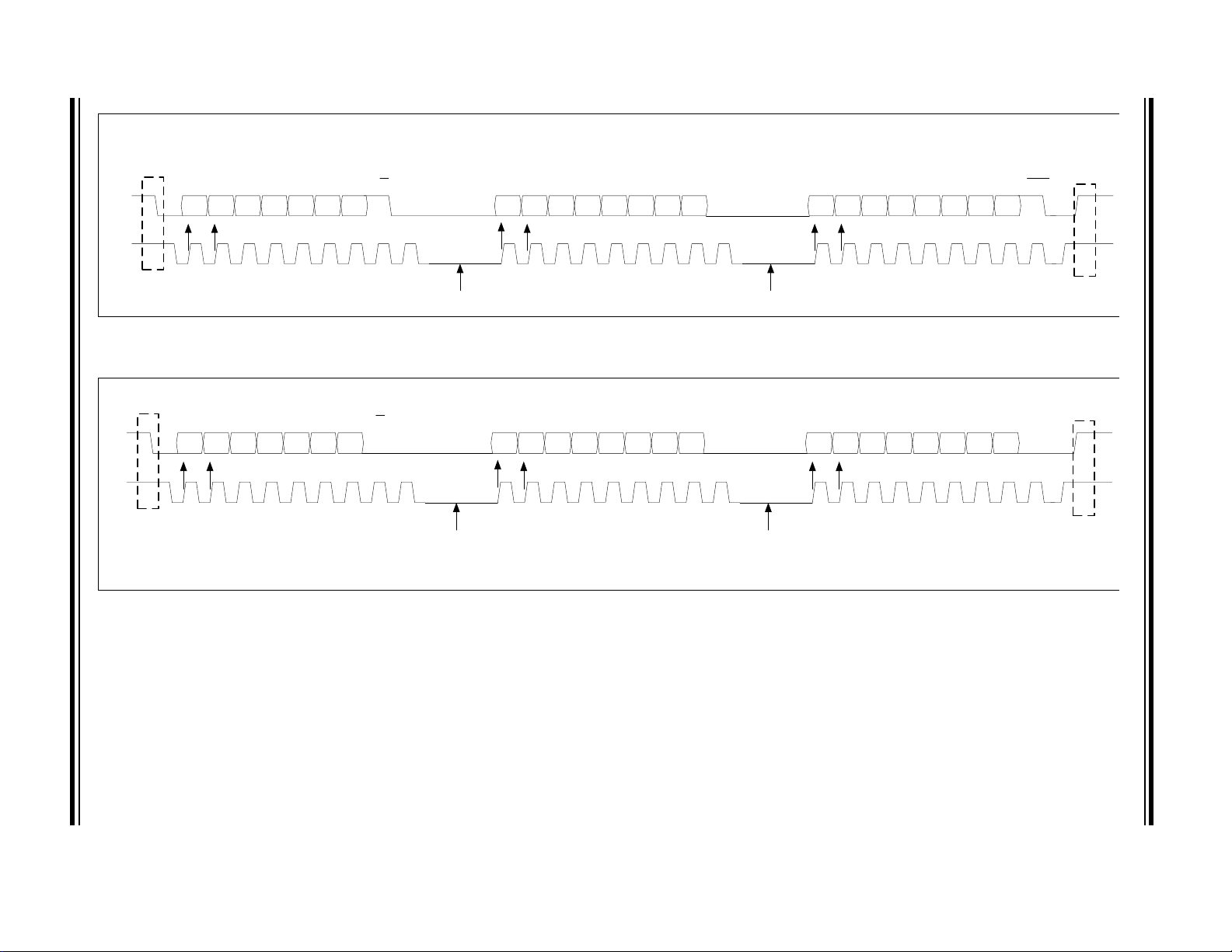
C Master Read Bit Timing (MGC3130 I2C Slave)
I
Master read is to receive position data, gesture reports
and command responses from the MGC3130. The
timing diagram is shown in Figure 6-4.
• Address bits are latched into the MGC3130 on the
rising edges of SCL.
• Data bits are latched out of the MGC3130 on the
rising edges of SCL.
• ACK bit:
- MGC3130 presents the ACK bit on the ninth
clock for address acknowledgment
2
C master presents the ACK bit on the ninth
-I
clock for data acknowledgment
•The I2C master must monitor the SCL pin prior to
asserting another clock pulse, as the MGC3130
may be holding off the I
the clock.
I2C Communication Steps
1. SCL and SDA lines are Idle high.
2
2. I
C master presents Start bit to the MGC3130 by
taking SDA high-to-low, followed by taking SCL
high-to-low.
3. I2C master presents 7-bit address, followed by a
= 1 (Read mode) bit to the MGC3130 on
R/W
SDA, at the rising edge of eight master clock
(SCL) cycles.
4. MGC3130 compares the received address to its
Device ID. If they match, the MGC3130
acknowledges (ACK) the master sent address
by presenting a low on SDA, followed by a lowhigh-low on SCL.
2
5. I
C master monitors SCL, as the MGC3130 may
be clock stretching, holding SCL low to indicate
that the I2C master should wait.
2
C master by stretching
DS40001667C-page 28 Advance Information 2012-2013 Microchip Technology Inc.
Page 29

MGC3130
6. I2C master receives eight data bits (MSB first)
presented on SDA by the MGC3130, at eight
sequential I2C master clock (SCL) cycles. The
data is latched out on SCL falling edges to
ensure it is valid during the subsequent SCL
high time.
7. If data transfer is not complete, then:
-I2C master acknowledges (ACK) reception of
the eight data bits by presenting a low on
SDA, followed by a low-high-low on SCL.
- Go to step 5.
8. If data transfer is complete, then:
-I2C master acknowledges (ACK) reception of
the eight data bits and a completed data
transfer by presenting a high on SDA,
followed by a low-high-low on SCL.
2
C Master Write Bit Timing (MGC3130 Slave)
I
I2C master write is to send supported commands to the
MGC3130. The timing diagram is shown in Figure 6-5.
• Address bits are latched into the MGC3130 on the
rising edges of SCL.
• Data bits are latched into the MGC3130 on the
rising edges of SCL.
• ACK bit:
- MGC3130 presents the ACK bit on the ninth
clock for address acknowledgment
2
C master presents the ACK bit on the ninth
-I
clock for data acknowledgment
• The master must monitor the SCL pin prior to
asserting another clock pulse, as the MGC3130
may be holding off the master by stretching the
clock.
I2C Communication Steps
1. SCL and SDA lines are Idle high.
2. I2C master presents Start bit to the MGC3130 by
taking SDA high-to-low, followed by taking SCL
high-to-low.
2
C master presents 7-bit address, followed by a
3. I
= 0 (Write mode) bit to the MGC3130 on
R/W
SDA, at the rising edge of eight master clock
(SCL) cycles.
4. MGC3130 compares the received address to its
Device ID. If they match, the MGC3130
acknowledges (ACK) the I
2
C master sent
address by presenting a low on SDA, followed
by a low-high-low on SCL.
5. I2C master monitors SCL, as the MGC3130 may
be clock stretching, holding SCL low to indicate
2
C master should wait.
the I
6. I2C master presents eight data bits (MSB first) to
the MGC3130 on SDA, at the rising edge of
eight master clock (SCL) cycles.
7. MGC3130 acknowledges (ACK) receipt of the
eight data bits by presenting a low on SDA, followed by a low-high-low on SCL.
8. If data transfer is not complete, then go to step
5.
9. Master presents a Stop bit to the MGC3130 by
taking SCL low-high, followed by taking SDA
low-to-high.
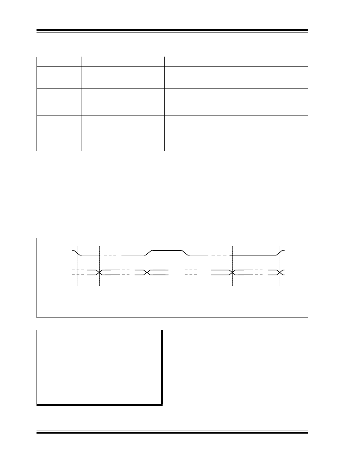
6.6.2 TRANSFER STATUS LINE
MGC3130 requires a dedicated Transfer Status line
(TS) which features a data transfer status function. It is
used by both I2C Master and Slave to control data flow.
The TS (Transfer Status) line is electrically open-drain
and requires a pull-up resistor of typically 10 k, from
TS to V
The MGC3130 (I
host controller (I
which can be transferred. The host controller uses the
TS line to indicate that data is being transferred and
prevents MGC3130 from updating its data buffer.
Table 6-9 shows how the TS line is used in the different
states of communication.
DD. TS Idle state is high.
2
C Slave) uses this line to inform the
2
C Master) that there is data available
2012-2013 Microchip Technology Inc. Advance Information DS40001667C-page 29
Page 30
MGC3130
Transfer Status
(TS)
I2CTM Bus
MGC3130 Related Transfer MGC3130 Related Transfer
TS line pulled
low by master
when transfer
is started
TS line released
by master and
MGC3130 when
transfer is
finished
TS line pulled
by MGC3130
to request a
data transfer
MGC3130 buffer
can be updated
Non MGC3130 related transfer or Bus Idle
TS line pulled
low by master
when transfer is
started
MGC3130 buffer
can be updated
TS line pulled
by MGC3130
to request a
data transfer
TS line released
by master and
MGC3130 when
transfer is
finished
TABLE 6-9: USAGE OF TRANSFER STATUS LINE
MGC3130 Host Controller TS Line Status
Released (H) Released (H) High Host finished reading data (Transfer end). No more data to
be transferred to the host. MGC3130 is allowed to update the
data buffer.
Asserted (L) Released (H) Low Data from MGC3130 is available to be sent, but the host has
not yet started reading. If the host is busy and did not start
reading before the next data update (5 ms), the MGC3130
will assert the TS line high while updating the data buffer.
Asserted (L) Asserted (L) Low Host starts reading. MGC3130 data buffer will not be updated
until the end of transfer (host releases TS high).
Released (H) Asserted (L) Low MGC3130 is ready to update the data buffer, but the host is
still reading the previous data. MGC3130 is allowed to
update the data only when the host releases the TS high.
MGC3130 can update the I2C buffer only when the TS
is released by both chips and a data transfer can only
be started when MGC3130 pulls the TS low.
This procedure secures that:
• the host is always informed when new sensor
data is available
• buffer updates in MGC3130 are always
completed before data is sent to the I
Figure 6-3 shows the complete communication
protocol.
2
C bus
FIGURE 6-3: MGC3130 COMMUNICATION PROTOCOL
Note 1: The stop condition after an I2C™ data
transmission is generated by the host
controller (I2C Master) after the data
transfer is completed. Thus, it is
recommended to verify the amount of
bytes to be read in the message header
(Size field).
2: Transfer Status is only needed for data
transfer from MGC3130 to the host controller. Writing to MGC3130 does not
require the additional TS signal.
In addition to the standard I2C interface, the
communication between MGC3130 and the host
controller requires a proper handling of the Transfer
Status.
DS40001667C-page 30 Advance Information 2012-2013 Microchip Technology Inc.
Page 31

6.6.3 SPI
SPI features:
• One Port: SCLK, CS, MOSI, MISO
• Master and Slave mode
• Up to 3 MHz
• Support of all clock edge and polarity options
2
Note: Currently, only single-zone I
mode with I
modes are planned for future releases of
GestIC
Microchip representative for further
details.
SPI Hardware Interface
A summary of the hardware interface pins is shown
below in Tab le 6 - 10 .
2
C0 is supported. Other
®
Library. Please contact your
C™ Slave
TABLE 6-10: SPI PIN DESCRIPTION
MGC3130 Pin Description
SCLK Master Clock
CS
MISO Master Input Slave Output
MOSI Master Output Slave Input
Chip Select
MGC3130
• SCLK Pin:
- The MGC3130 controller’s SCLK pin drives
the communication bus clock.
- The Idle state of the SCLK should be low.
- Data is transmitted on the falling edge of
SCLK.
•MOSI Pin:
- The MGC3130 controller’s MOSI pin sends/
reads serial data to/from the slave/host.
•MISO Pin:
- The MGC3130 controller’s MISO pin reads/
sends serial data from/to the slave/host.
Pin:
•CS
- The MGC3130 controller’s CS
device selection functionality.
pin provides
TABLE 6-11: SPI CS PIN DESCRIPTION
CS Pin Description
V
SS Active
VDD Inactive
2012-2013 Microchip Technology Inc. Advance Information DS40001667C-page 31
Page 32
DS40001667C-page 32 Advance Information 2012-2013 Microchip Technology Inc.
312 456789 312 456789 312 456789
A7 A6 A5 A4 A3 A2 A1
1
D7 D6 D5 D4 D3 D2 D1 D0 D7 D6 D5 D4 D3 D2 D1 D0
Address R/W ACK ACK ACKData Data
Address Bits Latched in Data Bits Valid Out Data Bits Valid Out
SCL may be stretched SCL may be stretched
S
P
Start Bit
Stop Bit
SDA
SCL
312 456789 312 456789 312 456789
A7 A6 A5 A4 A3 A2 A1
0
D7 D6 D5 D4 D3 D2 D1 D0 D7 D6 D5 D4 D3 D2 D1 D0
Address R/W ACK ACK ACKData Data
Address Bits Latched in Data Bits Valid Out Data Bits Valid Out
SCL may be stretched SCL may be stretched
S
P
Start Bit
Stop Bit
SDA
SCL
FIGURE 6-4: I2C™ MASTER READ BIT TIMING DIAGRAM
MGC3130
FIGURE 6-5: I
2
C™ MASTER WRITE BIT TIMING DIAGRAM
Page 33
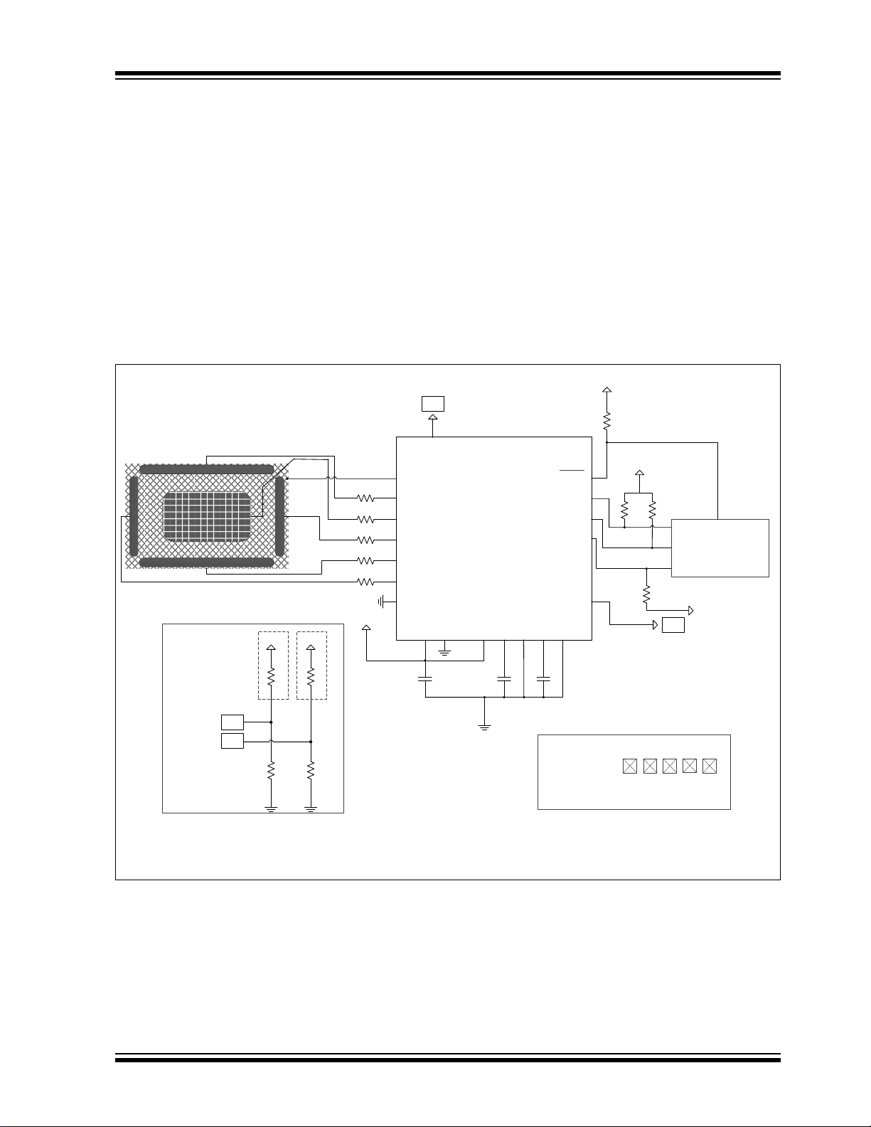
MGC3130
MGC3130
VDD
VSS1
VSS3
VDD
100 nF
4.7 μF
4.7 μF
IS2
MCLR
SI0
SI1
EIO0
SDA
SCL
GPIO/IRQ
HOST
VDD
1.8 kΩ
1.8 kΩ
RESET
10 kΩ
VDD
TXD
RX0
RX1
RX2
RX3
RX4
VDD
VINDS
VCAPS
VCAPA
VCAPD
EXP
VSS1
NC
NC
NC
VSS2
EIO7
EIO1
EIO6
NC
North Electrode
South Electrode
East Electrode
WestElectrode
Center Electrode
IS1
IS2
R9 (10 kΩ)
C1
C3
C2
R1
R2
R3
10 kΩ
10 kΩ
10 kΩ
10 kΩ
IS1
IS2
VDD VDD
R6
R8
R5 (n.p)
R7 (n.p)
R10 (10 kΩ)
R11 (10 kΩ)
R12 (10 kΩ)
R13 (10 kΩ)
VDD
10 kΩ
R4
EIO2
EIO3
n.p: not populated
Gesture Port
EIO7
EIO1
EIO6
EIO2
EIO3
Interface Selection
Note: R5 and R7 are not populated.
7.0 HARDWARE INTEGRATION
7.3 Irradiated High-Frequency Noise
In order to suppress irradiated high-frequency signals,
7.1 ESD Considerations
The MGC3130 provides Electrostatic Discharge (ESD)
Voltage protection up to 2 kV (HBM). Additional ESD
countermeasures may be implemented individually to
meet application-specific requirements.
7.2 Power Noise Considerations
the five Rx channels of the chip are connected to the
electrodes via serial 10 kresistors, as close as possible to MGC3130. The 10 k resistor and the MGC3130
input capacitance are building a low-pass filter with a
corner frequency of 3 MHz.
7.4 Standard Schematic
(3.3V V
DD 3.465V)
MGC3130 filtering capacitors are included in the
reference design schematic (Please refer to Figure 7-1).
A standard application schematic for the 28-lead QFN
package pinout is depicted below in Figure 7-1. For
more details, please refer to Figure 1.
FIGURE 7-1: STANDARD SCHEMATIC FOR 3.3V VDD 3.465V VOLTAGE RANGE
2012-2013 Microchip Technology Inc. Advance Information DS40001667C-page 33
Page 34
MGC3130
MGC3130
VDD
VSS1
VSS3
VDD
100 nF
4.7 μF
4.7 μF
MCLR
SDA
SCL
GPIO/IRQ
HOST
VDD
1.8 kΩ
1.8 kΩ
RESET
10 kΩ
VDD
TXD
RX0
RX1
RX2
RX3
RX4
VINDS
VCAPS
VCAPA
VCAPD
EXP
NC
NC
NC
VSS2
EIO7
IS2
SI0
SI1
EIO0
EIO1
EIO6
NC
10 μF
4.7 μH
IS2
IS1
North Electrode
South Electrode
East Electrode
WestElectrode
Center Electrode
C1
L1
C4
D1
C3
C2
R1
R2
R3
R9 (10 kΩ)
R10 (10 kΩ)
R11 (10 kΩ)
R12 (10 kΩ)
R13 (10 kΩ)
VDD
10 kΩ
R4
10 kΩ
10 kΩ
10 kΩ
10 kΩ
IS1
IS2
VDD VDD
R6
R8
R5 (n.p)
R7 (n.p)
n.p: not populated
Interface Selection
EIO2
EIO3
Gesture Port
EIO7
EIO1
EIO6
EIO2
EIO3
7.5 Bill of Materials (3.3V VDD
3.465V)
Modifying, removing or adding components may
adversely affect MGC3130 performance.
TABLE 7-1: BILL OF MATERIALS FOR 3.3V V
Label Qty Value Description
R1, R4, R5, R6, R7, R8 3 10 k Res Thick Film 10 k
C1 1 100 nF Capacitor – Ceramic, 0.1 µF, 10%, 6.3V
C2 1 4.7 µF Capacitor – Ceramic, 4.7 µF, 10%, 6.3V
C3 1 4.7 µF Capacitor – Ceramic, 4.7 µF, 10%, 6.3V
R2, R3 2 1.8 k Res Thick Film 1.8 k
R9, R10, R11, R12, R13 5 10 k Res Thick Film 10 k
7.6 Standard Schematic Step-Up
Setup (2.5V V
FIGURE 7-2: SCHEMATIC STEP-UP SETUP FOR 2.5V VDD 3.465V VOLTAGE RANGE
DD 3.465V)
DD 3.465V
DS40001667C-page 34 Advance Information 2012-2013 Microchip Technology Inc.
Page 35

MGC3130
7.7 Bill of Materials (2.5V VDD
3.465V)
Modifying, removing, or adding components may
adversely affect MGC3130 performance.
TABLE 7-2: BILL OF MATERIALS FOR 2.5V VDD 3.465V
Label Qty Value Description
R1, R4, R5, R6, R7, R8 3 10 k Res Thick Film 10 k
C1 1 100 nF Capacitor – Ceramic, 0.1 µF, 10%, 6.3V
C2 1 4.7 µF Capacitor – Ceramic, 4.7 µF, 10%, 6.3V
C3 1 4.7 µF Capacitor – Ceramic, 4.7 µF, 10%, 6.3V
R2, R3 2 1.8 k Res Thick Film 1.8 k
C4 1 10 µF Capacitor – Ceramic, 10 µF, 20%, 6.3V
L1 1 4.7 µH Inductor, 4.7 µH 20%
D1 1
R9, R10, R11, R12, R13 5 10 k Res Thick Film 10 k
—
7.8 Layout Recommendation
Diode Schottky, 20V, 0.5A
This section will provide a brief description of layout
hints for a proper system design.
The PCB layout requirements for MGC3130 follow the
general rules for a mixed signal design. In addition,
there are certain requirements to be considered for the
sensor signals and electrode feeding lines.
The chip should be placed as close as possible to the
electrodes to keep their feeding lines as short as
possible. Furthermore, it is recommended to keep
MGC3130 away from electrical and thermal sources
within the system.
Analog and digital signals should be separated from
each other during PCB layout in order to minimize
crosstalk.
The individual electrode feeding lines should be kept as
far as possible apart from each other.
DD lines should be routed as wide as possible. For
V
designs using the STEP-UP circuitry, the additional
components required should be placed as close as
possible to the MGC3130.
MGC3130 requires a proper ground connection on all
SS pins, including the exposed pad (pin 29).
V
2012-2013 Microchip Technology Inc. Advance Information DS40001667C-page 35
Page 36

MGC3130
8.0 DEVELOPMENT SUPPORT
Microchip provides software and hardware
development tools for the MGC3130:
• Software:
- MGC3130 Software Package – Aurea GUI
and GestIC Library
- MGC3130 Software Development Kit (SDK)
- MGC3130 PIC18F14K50 Host Reference
Code
•Schematics:
- MGC3130 Hillstar Hardware References
• Evaluation and Development Kits:
- MGC3130 – Sabrewing Single-Zone
Evaluation Kit (DM160217)
- MGC3130 Single-Zone Development Kit
Hillstar (DM160218)
8.1 MGC3130 Software Package – Aurea GUI and GestIC Library
The Aurea evaluation software demonstrates
Microchip’s GestIC
applications. Aurea provides visualization of the
MGC3130 generated data and access to GestIC
Library controls and configuration parameters.
That contains the following:
• Visualization of hand position and user gestures
• Visualization of sensor data
• Real-time control of sensor features
• MGC3130 GestIC Library update
• Analog front end parameterization
• Colibri parameterization
• Electrode capacitance measurement
• Logging of sensor values and storage in a log file
®
technology and its features and
8.4 MGC3130 Hillstar Hardware References
Microchip provides the Gerber files for Hillstar Boards
and Reference electrodes.
8.5 Evaluation and Demonstration Kits
A variety of demonstration, development and
evaluation boards allow quick application development
on fully-functional systems. The demonstration and
development boards can be used in teaching
environments, for prototyping custom circuits and for
learning about various GestIC MGC3130 applications.
The first MGC3130 evaluation board is the Sabrewing
Single-Zone Evaluation Board. It contains the
MGC3130 reference circuitry and built-in frame
electrodes with a 140 x 90 mm sensitive area.
In combination with Aurea Visualization and Control
Software, Sabrewing can be used as a starter kit. The
set contains all materials required for first MGC3130
evaluation experience.
The first development board is the Hillstar
Development Kit. It is designed to support an easy
integration of Microchip’s MGC3130 3D Tracking and
Gesture Controller into the customer’s applications. It
provides MGC3130 system hardware modules and a
set of electrode reference designs which can be used
by customers to develop their own GestIC system.
Aurea Visualization and Control Software provides full
support of the Hillstar Development Kit and an easy
parameterization of the customer’s applications.
For the complete list of demonstration, development
and evaluation kits, please refer to the Microchip web
site (http://www.microchip.com/GestICGettingStarted).
8.2 MGC3130 Software Development Kit (SDK)
Microchip provides a standard C reference code with a
Software Development Kit. The code will support
developers to integrate the MGC3130 solution into the
target application.
8.3 MGC3130 PIC18F14K50 Host Reference Code
Microchip provides a reference code for PIC18F14K50,
including GestIC Library I
decoding.
DS40001667C-page 36 Advance Information 2012-2013 Microchip Technology Inc.
2
C code and basic message
8.6 GestIC Library Update
The MGC3130 devices are manufactured only with a
built-in Library Loader to perform basic device programming operations or individual configuration
parameters storage over a serial I
The user has to download the latest GestIC Library and
upload it to the MGC3130 Flash memory.
The GestIC Library can be updated through two
methods:
1. Aurea Visualization and Control Software:
Please refer to MGC3130 Aurea Graphical User
Interface User Guide (DS40001681) for more
details.
2. GestIC Library messages: Please refer to
MGC3130 GestIC Library Interface Description
User Guide (DS40001718) for more details.
2
C interface.
Page 37

9.0 ELECTRICAL SPECIFICATIONS
MGC3130
9.1 Absolute Maximum Ratings
Ambient temperature under bias......................................................................................................... -20°C to +85°C
Storage temperature ........................................................................................................................ -55°C to +125°C
Voltage on pins with respect to V
on VDD pin ............................................................................................................................ -0.3V to +3.465V
on all other pins.............................................................................................................. -0.3V to (V
Total power dissipation................................................................................................................................... 100 mW
ESD protection on all pins .................................................................................................................................... 2 kV
† NOTICE: Stresses above those listed under “Absolute Maximum Ratings” may cause permanent damage to the
device. This is a stress rating only and functional operation of the device at those or any other conditions above
those indicated in the operation listings of this specification is not implied. Exposure to maximum rating conditions for
extended periods may affect device reliability.
† NOTICE: This device is sensitive to ESD damage and must be handled appropriately. Failure to properly handle
and protect the device in an application may cause partial to complete failure of the device.
† NOTICE: -20°C temperature operation is characterized but not tested.
SS
(†)
DD + 0.3V)
2012-2013 Microchip Technology Inc. Advance Information DS40001667C-page 37
Page 38
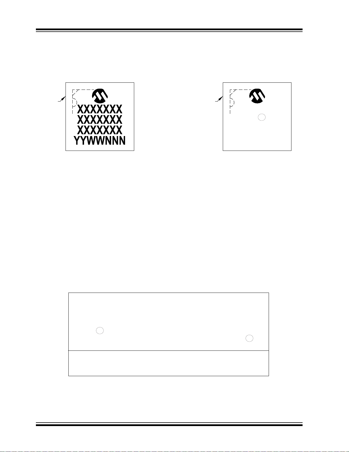
MGC3130
28-Lead QFN (5x5x0.9 mm) Example
PIN 1 PIN 1
MGC3130
-I/MQ
1318017
3
e
Legend: XX...X Customer-specific information
Y Year code (last digit of calendar year)
YY Year code (last 2 digits of calendar year)
WW Week code (week of January 1 is week ‘01’)
NNN Alphanumeric traceability code
Pb-free JEDEC
®
designator for Matte Tin (Sn)
* This package is Pb-free. The Pb-free JEDEC designator ( )
can be found on the outer packaging for this package.
Note: In the event the full Microchip part number cannot be marked on one line, it will
be carried over to the next line, thus limiting the number of available
characters for customer-specific information.
3
e
10.0 PACKAGING INFORMATION
10.1 Package Marking Information
3
e
DS40001667C-page 38 Advance Information 2012-2013 Microchip Technology Inc.
Page 39
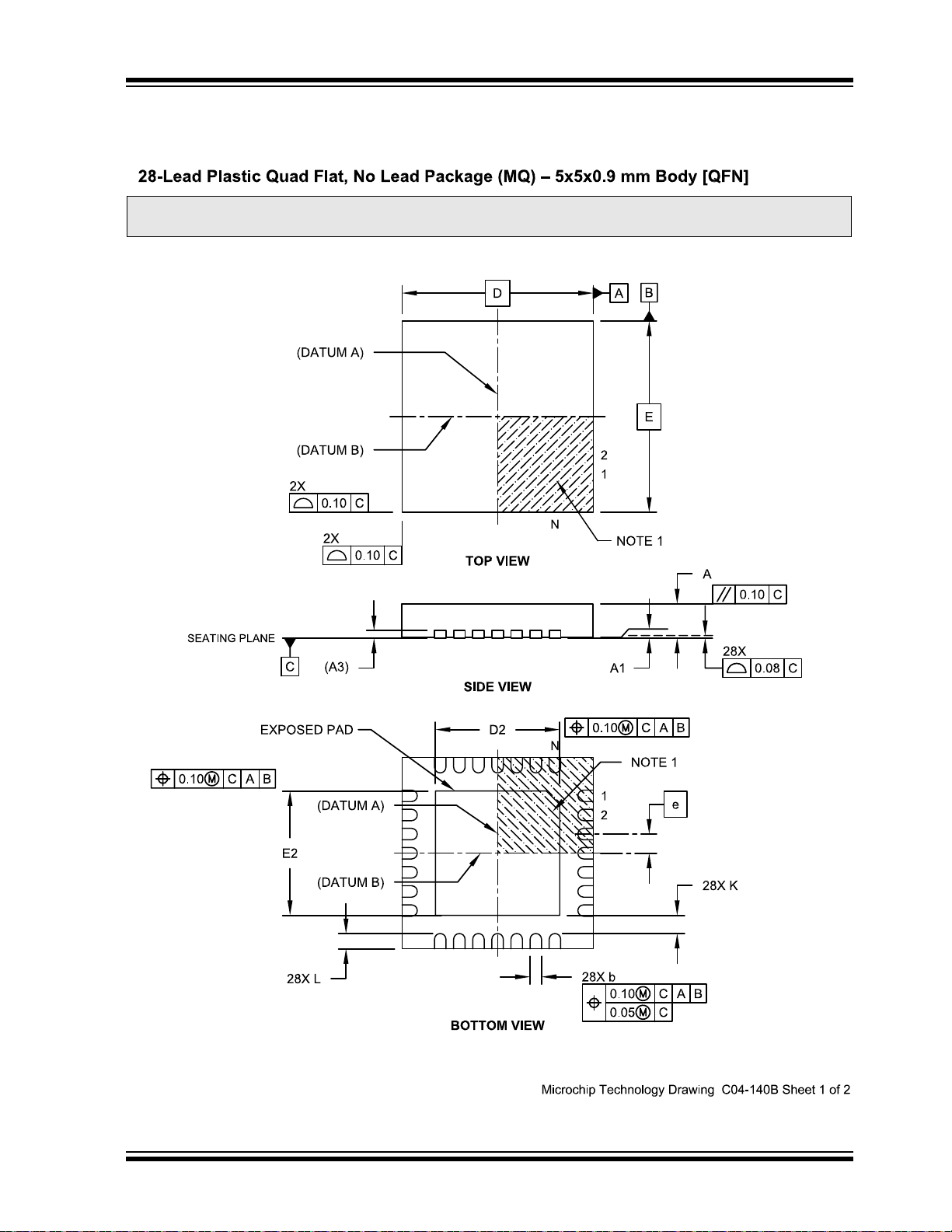
10.2 Package Details
Note: For the most current package drawings, please see the Microchip Packaging Specification located at
http://www.microchip.com/packaging
The following sections give the technical details of the packages.
MGC3130
2012-2013 Microchip Technology Inc. Advance Information DS40001667C-page 39
Page 40

MGC3130
Note: For the most current package drawings, please see the Microchip Packaging Specification located at
http://www.microchip.com/packaging
DS40001667C-page 40 Advance Information 2012-2013 Microchip Technology Inc.
Page 41
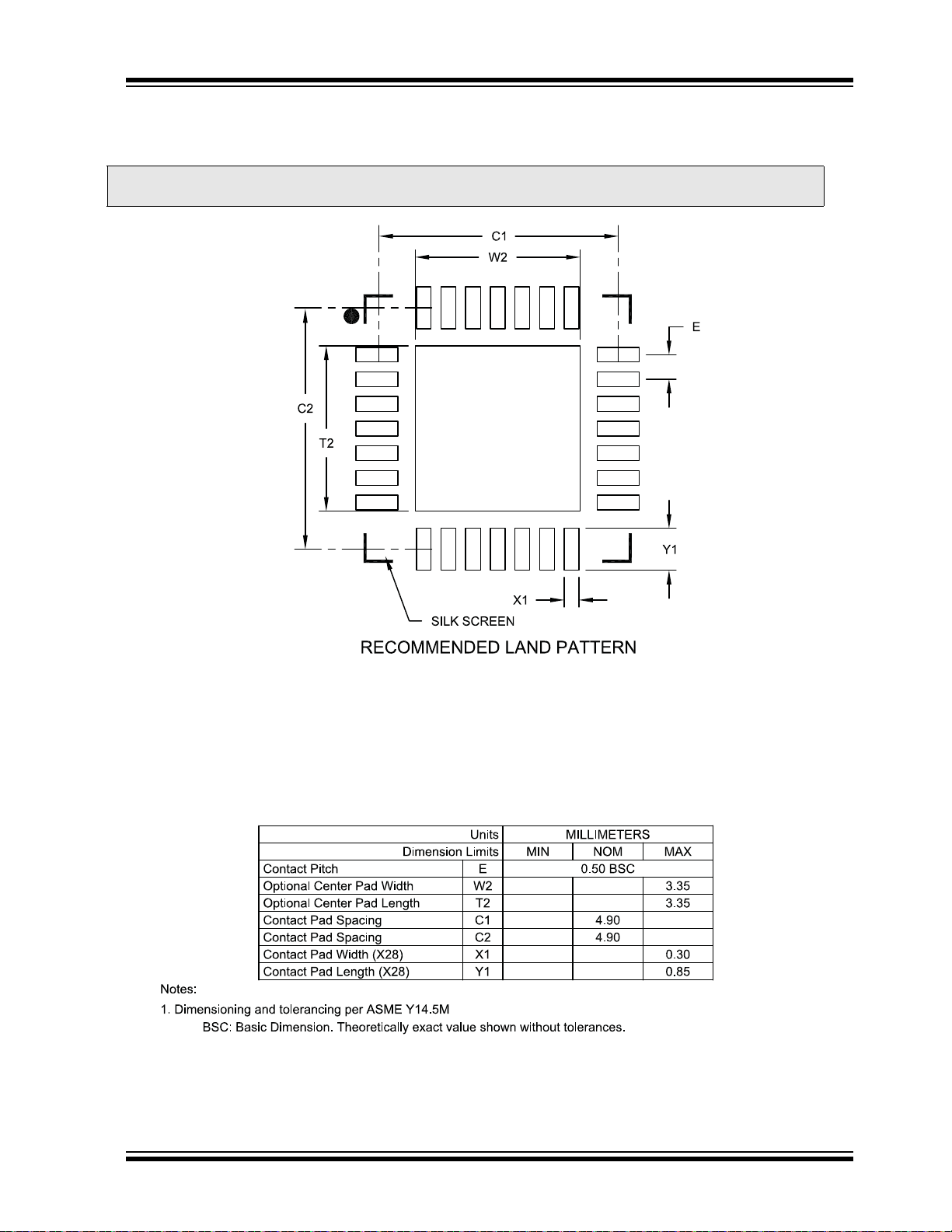
28-Lead Plastic Quad Flat, No Lead Package (MQ) – 5x5 mm Body [QFN] Land Pattern
With 0.55 mm Contact Length
Note: For the most current package drawings, please see the Microchip Packaging Specification located at
http://www.microchip.com/packaging
Microchip Technology Drawing C04-2140A
MGC3130
2012-2013 Microchip Technology Inc. Advance Information DS40001667C-page 41
Page 42

MGC3130
APPENDIX A: DATA SHEET
REVISION HISTORY
Revision A (11/2012)
Initial release of this data sheet.
Revision B (08/2013)
Updated the Power Features section; Updated Table 1;
Updated section 2, Feature Description; Updated section 4.2.2; Updated Figures 4-4, 4-5 and 4-6; Updated
Equation 4-1, Table 4-1; Updated Figures 4-9, 5-1 and
5-2; Updated section 6, Interface Description, Updated
Figures 7-1 and 7-2; Added section 7-3, Irradiated
High-Frequency Noise; Updated Tables 7-1 and 7-2;
Updated section 8, Development Support; Updated the
Packaging Information section; Other minor corrections.
Revision C (11/2013)
Updated Figure 1 and Table 1; Updated Section 2,
Feature Description; Updated Section 4, Functional
Description; Updated Section 6, Interface Description;
Updated Figure 7-1 and 7-2; Updated Section 8,
Development Support; Other minor corrections.
DS40001667C-page 42 Advance Information 2012-2013 Microchip Technology Inc.
Page 43

MGC3130
THE MICROCHIP WEB SITE
Microchip provides online support via our WWW site at
www.microchip.com. This web site is used as a means
to make files and information easily available to
customers. Accessible by using your favorite Internet
browser, the web site contains the following
information:
• Product Support – Data sheets and errata,
application notes and sample programs, design
resources, user’s guides and hardware support
documents, latest software releases and archived
software
• General Technical Support – Frequently Asked
Questions (FAQ), technical support requests,
online discussion groups, Microchip consultant
program member listing
• Business of Microchip – Product selector and
ordering guides, latest Microchip press releases,
listing of seminars and events, listings of
Microchip sales offices, distributors and factory
representatives
CUSTOMER CHANGE NOTIFICATION SERVICE
CUSTOMER SUPPORT
Users of Microchip products can receive assistance
through several channels:
• Distributor or Representative
• Local Sales Office
• Field Application Engineer (FAE)
• Technical Support
Customers should contact their distributor,
representative or Field Application Engineer (FAE) for
support. Local sales offices are also available to help
customers. A listing of sales offices and locations is
included in the back of this document.
Technical support is available through the web site
at: http://microchip.com/support
Microchip’s customer notification service helps keep
customers current on Microchip products. Subscribers
will receive e-mail notification whenever there are
changes, updates, revisions or errata related to a
specified product family or development tool of interest.
To register, access the Microchip web site at
www.microchip.com. Under “Support”, click on
“Customer Change Notification” and follow the
registration instructions.
2012-2013 Microchip Technology Inc. Advance Information DS40001667C-page 43
Page 44
MGC3130
PART NO. X /XX XXX
PatternPackageTemperature
Range
Device
Device: MGC3130
Tape and Reel
Option:
Blank = Standard packaging (tube or tray)
T = Tape and Reel
(1)
Temperature
Range:
I= -40C to +85C (Industrial)
Package:
(2)
MQ = QFN
Pattern: QTP, SQTP, Code or Special Requirements
(blank otherwise)
Examples:
a) MGC3130 - I/MQ
Industrial temperature,
QFN package
Note 1: Tape and Reel identifier only appears in the
catalog part number description. This
identifier is used for ordering purposes and is
not printed on the device package. Check
with your Microchip Sales Office for package
availability with the Tape and Reel option.
2: For other small form-factor package
availability and marking information, please
visit www.microchip.com/packaging or
contact your local sales office.
[X]
(1)
Tape and Reel
Option
-
PRODUCT IDENTIFICATION SYSTEM
To order or obtain information, e.g., on pricing or delivery, refer to the factory or the listed sales office.
DS40001667C-page 44 Advance Information 2012-2013 Microchip Technology Inc.
Page 45

Note the following details of the code protection feature on Microchip devices:
YSTEM
CERTIFIED BY DNV
== ISO/TS 16949 ==
• Microchip products meet the specification contained in their particular Microchip Data Sheet.
• Microchip believes that its family of products is one of the most secure families of its kind on the market today, when used in the
intended manner and under normal conditions.
• There are dishonest and possibly illegal methods used to breach the code protection feature. All of these methods, to our
knowledge, require using the Microchip products in a manner outside the operating specifications contained in Microchip’s Data
Sheets. Most likely, the person doing so is engaged in theft of intellectual property.
• Microchip is willing to work with the customer who is concerned about the integrity of their code.
• Neither Microchip nor any other semiconductor manufacturer can guarantee the security of their code. Code protection does not
mean that we are guaranteeing the product as “unbreakable.”
Code protection is constantly evolving. We at Microchip are committed to continuously improving the code protection features of our
products. Attempts to break Microchip’s code protection feature may be a violation of the Digital Millennium Copyright Act. If such acts
allow unauthorized access to your software or other copyrighted work, you may have a right to sue for relief under that Act.
Information contained in this publication regarding device
applications and the like is provided only for your convenience
and may be superseded by updates. It is your responsibility to
ensure that your application meets with your specifications.
MICROCHIP MAKES NO REPRESENTATIONS OR
WARRANTIES OF ANY KIND WHETHER EXPRESS OR
IMPLIED, WRITTEN OR ORAL, STATUTORY OR
OTHERWISE, RELATED TO THE INFORMATION,
INCLUDING BUT NOT LIMITED TO ITS CONDITION,
QUALITY, PERFORMANCE, MERCHANTABILITY OR
FITNESS FOR PURPOSE
arising from this information and its use. Use of Microchip
devices in life support and/or safety applications is entirely at
the buyer’s risk, and the buyer agrees to defend, indemnify and
hold harmless Microchip from any and all damages, claims,
suits, or expenses resulting from such use. No licenses are
conveyed, implicitly or otherwise, under any Microchip
intellectual property rights.
. Microchip disclaims all liability
Trademarks
The Microchip name and logo, the Microchip logo, dsPIC,
FlashFlex, K
PICSTART, PIC
and UNI/O are registered trademarks of Microchip Technology
Incorporated in the U.S.A. and other countries.
FilterLab, Hampshire, HI-TECH C, Linear Active Thermistor,
MTP, SEEVAL and The Embedded Control Solutions
Company are registered trademarks of Microchip Technology
Incorporated in the U.S.A.
Silicon Storage Technology is a registered trademark of
Microchip Technology Inc. in other countries.
Analog-for-the-Digital Age, Application Maestro, BodyCom,
chipKIT, chipKIT logo, CodeGuard, dsPICDEM,
dsPICDEM.net, dsPICworks, dsSPEAK, ECAN,
ECONOMONITOR, FanSense, HI-TIDE, In-Circuit Serial
Programming, ICSP, Mindi, MiWi, MPASM, MPF, MPLAB
Certified logo, MPLIB, MPLINK, mTouch, Omniscient Code
Generation, PICC, PICC-18, PICDEM, PICDEM.net, PICkit,
PICtail, REAL ICE, rfLAB, Select Mode, SQI, Serial Quad I/O,
Total Endurance, TSHARC, UniWinDriver, WiperLock, ZENA
and Z-Scale are trademarks of Microchip Technology
Incorporated in the U.S.A. and other countries.
SQTP is a service mark of Microchip Technology Incorporated
in the U.S.A.
GestIC and ULPP are registered trademarks of Microchip
Technology Germany II GmbH & Co. KG, a subsidiary of
Microchip Technology Inc., in other countries.
All other trademarks mentioned herein are property of their
respective companies.
© 2012-2013, Microchip Technology Incorporated, Printed in
the U.S.A., All Rights Reserved.
Printed on recycled paper.
ISBN: 9781620776612
EELOQ, KEELOQ logo, MPLAB, PIC, PICmicro,
32
logo, rfPIC, SST, SST Logo, SuperFlash
QUALITY MANAGEMENT S
2012-2013 Microchip Technology Inc. Advance Information DS40001667C-page 45
Microchip received ISO/TS-16949:2009 certification for its worldwide
headquarters, design and wafer fabrication facilities in Chandler and
Tempe, Arizona; Gresham, Oregon and design centers in California
and India. The Company’s quality system processes and procedures
are for its PIC
devices, Serial EEPROMs, microperipherals, nonvolatile memory and
analog products. In addition, Microchip’s quality system for the design
and manufacture of development systems is ISO 9001:2000 certified.
®
MCUs and dsPIC® DSCs, KEELOQ
®
code hopping
Page 46

Worldwide Sales and Service
AMERICAS
Corporate Office
2355 West Chandler Blvd.
Chandler, AZ 85224-6199
Tel: 480-792-7200
Fax: 480-792-7277
Technical Support:
http://www.microchip.com/
support
Web Address:
www.microchip.com
Atlanta
Duluth, GA
Tel: 678-957-9614
Fax: 678-957-1455
Austin, TX
Tel: 512-257-3370
Boston
Westborough, MA
Tel: 774-760-0087
Fax: 774-760-0088
Chicago
Itasca, IL
Tel: 630-285-0071
Fax: 630-285-0075
Cleveland
Independence, OH
Tel: 216-447-0464
Fax: 216-447-0643
Dallas
Addison, TX
Tel: 972-818-7423
Fax: 972-818-2924
Detroit
Novi, MI
Tel: 248-848-4000
Houston, TX
Tel: 281-894-5983
Indianapolis
Noblesville, IN
Tel: 317-773-8323
Fax: 317-773-5453
Los Angeles
Mission Viejo, CA
Tel: 949-462-9523
Fax: 949-462-9608
New York, NY
Tel: 631-435-6000
San Jose, CA
Tel: 408-735-9110
Canada - Toronto
Tel: 905-673-0699
Fax: 905-673-6509
ASIA/PACIFIC
Asia Pacific Office
Suites 3707-14, 37th Floor
Tower 6, The Gateway
Harbour City, Kowloon
Hong Kong
Tel: 852-2401-1200
Fax: 852-2401-3431
Australia - Sydney
Tel: 61-2-9868-6733
Fax: 61-2-9868-6755
China - Beijing
Tel: 86-10-8569-7000
Fax: 86-10-8528-2104
China - Chengdu
Tel: 86-28-8665-5511
Fax: 86-28-8665-7889
China - Chongqing
Tel: 86-23-8980-9588
Fax: 86-23-8980-9500
China - Hangzhou
Tel: 86-571-2819-3187
Fax: 86-571-2819-3189
China - Hong Kong SAR
Tel: 852-2943-5100
Fax: 852-2401-3431
China - Nanjing
Tel: 86-25-8473-2460
Fax: 86-25-8473-2470
China - Qingdao
Tel: 86-532-8502-7355
Fax: 86-532-8502-7205
China - Shanghai
Tel: 86-21-5407-5533
Fax: 86-21-5407-5066
China - Shenyang
Tel: 86-24-2334-2829
Fax: 86-24-2334-2393
China - Shenzhen
Tel: 86-755-8864-2200
Fax: 86-755-8203-1760
China - Wuhan
Tel: 86-27-5980-5300
Fax: 86-27-5980-5118
China - Xian
Tel: 86-29-8833-7252
Fax: 86-29-8833-7256
China - Xiamen
Tel: 86-592-2388138
Fax: 86-592-2388130
China - Zhuhai
Tel: 86-756-3210040
Fax: 86-756-3210049
ASIA/PACIFIC
India - Bangalore
Tel: 91-80-3090-4444
Fax: 91-80-3090-4123
India - New Delhi
Tel: 91-11-4160-8631
Fax: 91-11-4160-8632
India - Pune
Tel: 91-20-3019-1500
Japan - Osaka
Tel: 81-6-6152-7160
Fax: 81-6-6152-9310
Japan - Tokyo
Tel: 81-3-6880- 3770
Fax: 81-3-6880-3771
Korea - Daegu
Tel: 82-53-744-4301
Fax: 82-53-744-4302
Korea - Seoul
Tel: 82-2-554-7200
Fax: 82-2-558-5932 or
82-2-558-5934
Malaysia - Kuala Lumpur
Tel: 60-3-6201-9857
Fax: 60-3-6201-9859
Malaysia - Penang
Tel: 60-4-227-8870
Fax: 60-4-227-4068
Philippines - Manila
Tel: 63-2-634-9065
Fax: 63-2-634-9069
Singapore
Tel: 65-6334-8870
Fax: 65-6334-8850
Taiwan - Hsin Chu
Tel: 886-3-5778-366
Fax: 886-3-5770-955
Taiwan - Kaohsiung
Tel: 886-7-213-7830
Taiwan - Taipei
Tel: 886-2-2508-8600
Fax: 886-2-2508-0102
Thailand - Bangkok
Tel: 66-2-694-1351
Fax: 66-2-694-1350
EUROPE
Austria - Wels
Tel: 43-7242-2244-39
Fax: 43-7242-2244-393
Denmark - Copenhagen
Tel: 45-4450-2828
Fax: 45-4485-2829
France - Paris
Tel: 33-1-69-53-63-20
Fax: 33-1-69-30-90-79
Germany - Dusseldorf
Tel: 49-2129-3766400
Germany - Munich
Tel: 49-89-627-144-0
Fax: 49-89-627-144-44
Germany - Pforzheim
Tel: 49-7231-424750
Italy - Milan
Tel: 39-0331-742611
Fax: 39-0331-466781
Italy - Venice
Tel: 39-049-7625286
Netherlands - Drunen
Tel: 31-416-690399
Fax: 31-416-690340
Poland - Warsaw
Tel: 48-22-3325737
Spain - Madrid
Tel: 34-91-708-08-90
Fax: 34-91-708-08-91
Sweden - Stockholm
Tel: 46-8-5090-4654
UK - Wokingham
Tel: 44-118-921-5800
Fax: 44-118-921-5820
10/28/13
DS40001667C-page 46 Advance Information 2013 Microchip Technology Inc.
 Loading...