

Page 1
MGP15N35CL,
MGB15N35CL,
MGC15N35CL
Internally Clamped
N-Channel IGBT
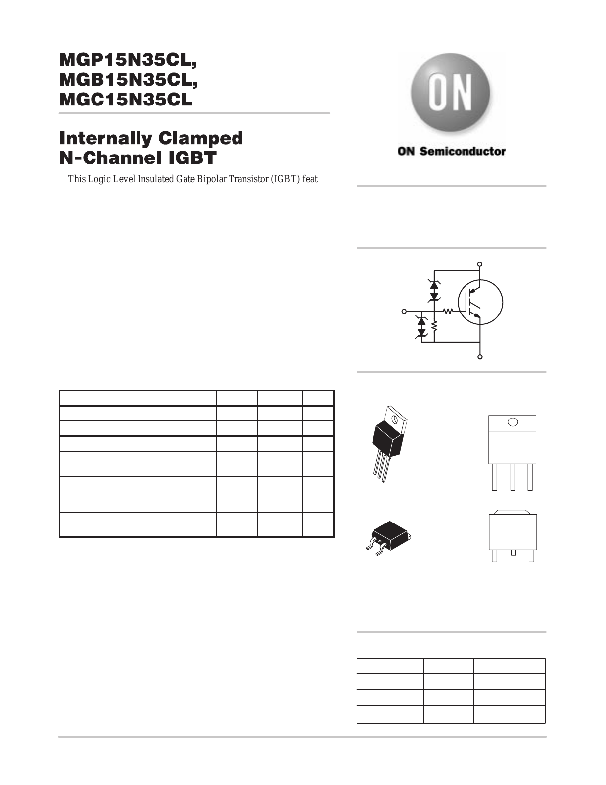
This Logic Level Insulated Gate Bipolar Transistor (IGBT) features
monolithic circuitry integrating ESD and Over–Voltage clamped
protection for use in inductive coil drivers applications. Primary uses
include Ignition, Direct Fuel Injection, or wherever high voltage and
high current switching is required.
• Gate–Emitter ESD Protection
• T emperature Compensated Gate–Collector Voltage Clamp Limits
Stress Applied to Load
• Integrated ESD Diode Protection
• Low Threshold Voltage to Interface Power Loads to Logic or
Microprocessor Devices
• Low Saturation Voltage
• High Pulsed Current Capability
• Optional Gate Resistor (R
)
G
http://onsemi.com
N–CHANNEL IGBT
15 A, 350 V
V
CE(on)
G
= 1.8 V MAX
C
R
G
R
GE
E
MAXIMUM RATINGS (T
Rating
Collector–Emitter Voltage V
Collector–Gate Voltage V
Gate–Emitter Voltage V
Collector Current–Continuous
@ TC = 25°C
Total Power Dissipation
@ TC = 25°C
Derate above 25°C
Operating and Storage Temperature
Range
= 25°C unless otherwise noted)
J
Symbol Value Unit
CES
CER
P
TJ, T
GE
I
C
D
stg
380 V
380 V
22 V
15 A
136
1.0
–55 to
175
DC
DC
DC
DC
Watts
W/°C
°C
MARKING
DIAGRAMS
TO–220
CASE 221A
STYLE 9
G
C
E
D2PAK
CASE 418B
STYLE 3
A = Assembly Location
WL, L = Wafer Lot
YY, Y = Year
WW, W= Work Week
ORDERING INFORMATION
Device Package Shipping
MGP15N35CL TO–220 50 Units/Rail
MGB15N35CL T4 D2PAK 800 Tape & Reel
MGC15N35CL Die Options
GP15N35CL
ALYYWW
GB15N35CL
ALYYWW
Not Applicable
Semiconductor Components Industries, LLC, 2000
April, 2000 – Rev. 0
1 Publication Order Number:
MGP15N35CL/D
Page 2
MGP15N35CL, MGB15N35CL, MGC15N35CL
UNCLAMPED DRAIN–TO–SOURCE AVALANCHE CHARACTERISTICS (TJ t150°C)
Characteristic Symbol Value Unit
Single Pulse Collector–to–Emitter Avalanche Energy
VCC = 50 V, VGE = 5 V, Pk IL = 14.2 A, L = 3 mH, Starting TJ = 25°C
VCC = 50 V, VGE = 5 V, Pk IL = 10 A, L = 3 mH, Starting TJ = 150°C
THERMAL CHARACTERISTICS
Characteristic Symbol Value Unit
Thermal Resistance, Junction to Case R
Thermal Resistance, Junction to Ambient TO–220 R
D2PAK R
Maximum Lead Temperature for Soldering Purposes, 1/8″ from case for 5 seconds T
E
AS
θJC
θJA
θJA
L
300
mJ
150
1.0 °C/W
62.5
50
275 °C
ELECTRICAL CHARACTERISTICS (T
Characteristic
= 25°C unless otherwise noted)
C
Symbol Test Conditions Min Typ Max Unit
OFF CHARACTERISTICS
Collector–Emitter Clamp V oltage BV
Zero Gate Voltage Collector Current I
Reverse Collector–Emitter Leakage Current I
Gate–Emitter Clamp Voltage BV
Gate–Emitter Leakage Current I
Gate Resistor (Optional) R
Gate Emitter Resistor R
CES
CES
ECS
GES
GES
G
GE
IC = 2 mA
TJ = –40°C to 175°C
VCE = 300 V,
VGE = 0, TJ = 25°C
VCE = 300 V,
VGE = 0, TJ = 150°C
VCE = –24 V – – 1.0 mA
IG = 5 mA 17 – 22 V
VGE = 10 V 384 – 1000 µA
– – 70 –
– 10 – 26
320 350 380 V
– – 40
– – 200
ON CHARACTERISTICS*
Gate Threshold Voltage V
Threshold Temperature Coefficient (Negative) – – – 4.4 – mV/°C
Collector–to–Emitter On–Voltage V
Collector–to–Emitter On–Voltage V
Forward Transconductance gfs VCE = 5 V, IC = 6 A 8.0 15 – Mhos
GE(th)
CE(on)
CE(on)
IC = 1 mA
VGE = V
IC = 6 A, VGE = 4 V – – 1.8 V
VGE = 4.5 V,
TJ = 150°C
CE
IC = 10 A,
1.0 1.8 2.1 V
– – 1.8 V
DYNAMIC CHARACTERISTICS
Input Capacitance C
Output Capacitance C
Transfer Capacitance C
*Pulse Test: Pulse Width v 300 µS, Duty Cycle v 2%.
ISS
OSS
RSS
VCC = 15 V – 1000 –
VGE = 0 V – 130 –
f = 1 MHz – 5.0 –
µA
DC
DC
DC
DC
Ω
kΩ
DC
DC
DC
pF
http://onsemi.com
2
Page 3
MGP15N35CL, MGB15N35CL, MGC15N35CL
ELECTRICAL CHARACTERISTICS (T
Characteristic
= 25°C unless otherwise noted)
C
SWITCHING CHARACTERISTICS*
Turn–Off Delay Time t
Fall Time t
Turn–On Delay Time t
Rise Time t
Gate Charge
*Pulse Test: Pulse Width v 300 µS, Duty Cycle v 2%.
Symbol Test Conditions Min Typ Max Unit
d(off)
f
d(on)
r
Q
T
Q
1
Q
2
VCC = 300 V,
IC = 10 A
RG = 1 kΩ,
L = 300 µH
VCC = 10 V,
IC = 6.5 A
RG = 1 kΩ,
RL = 1 Ω
VCC = 300 V – TBD –
IC = 15 A – TBD –
VGE = 5 V – TBD –
– 13 –
– 6.0 –
– 1.0 –
– 5.0 –
µSec
µSec
nC
http://onsemi.com
3
Page 4

MGP15N35CL, MGB15N35CL, MGC15N35CL
45
VGE = 10.0 V
40
VGE = 5.0 V
35
30
25
20
15
10
, COLLECTOR CURRENT (AMPS)
5
C
I
0
012345678
V
COLLECTOR TO EMITTER VOLTAGE (VOLTS)
CE,
VGE = 4.0 V
VGE = 3.0 V
Tj = 25°C
Figure 1. Output Characteristics Figure 2. Output Characteristics
30
VCE = 10 V
25
20
15
10
5
, COLLECTOR CURRENT (AMPS)
C
I
0
0 0.5 1 1.5 2 2.5 3 3.5 4
V
GE,
Tj = 150°C
Tj = 25°CT
GATE T O EMITTER VOLTAGE (VOLTS) Tj, JUNCTION TEMPERATURE (°C)
= 40°C
j
45
40
35
30
25
20
15
10
, COLLECTOR CURRENT (AMPS)
5
C
I
0
2.0
1.8
1.5
1.3
1.0
0.8
0.5
0.3
0.0
, COLLECTOR TO EMITTER VOLTAGE (VOLTS)
CE
V
VGE = 10.0 V
VGE = 5.0 V
012345678
V
COLLECTOR TO EMITTER VOLTAGE (VOLTS)
CE,
IC = 15 A
IC = 10 A
IC = 5 A
VGE = 15 V
–50 –25 0 25 50 75 100 125 1504.5 5
VGE = 4.0 V
VGE = 3.0 V
Tj = 150°C
Figure 3. Transfer Characteristics Figure 4. Collector–to–Emitter Saturation V oltage
10000
C
1000
100
C, CAPACITANCE (pF)
ISS
C
OSS
10
C
RSS
1
0 20 40 60 80 100 120 140 160 180 200
V
COLLECTOR TO EMITTER VOLTAGE (VOLTS)
CE,
Figure 5. Capacitance Variation Figure 6. Threshold V oltage versus Temperature
2.5
2.0
1.5
1.0
0.5
THRESHOLD VOLTAGE (VOLTS)
0.0
–50 –25 0 25 50 75 100 125 150
http://onsemi.com
4
versus Junction T emperature
Mean + 4 σ
Mean
Mean – 4 σ
TEMPERATURE (°C)
IC = 1 mA
Page 5

MGP15N35CL, MGB15N35CL, MGC15N35CL
20
VCC = 300 V
18
VGE = 5.0 V
16
S)SWITCHING TIME (
Tj = 25°C
m
IC = 10 A
14
L = 300 µH
12
10
8
6
4
2
0
250 500 750 1000
RG, GATE RESISTANCE (OHMS) RG, GATE RESISTANCE (OHMS)
t
d(off)
t
f
20
18
16
S)SWITCHING SPEED (
m
14
12
10
8
6
4
2
0
250 500 750 1000
t
d(off)
t
f
VCC = 300 V
VGE = 5.0 V
Tj = 150°C
IC = 10 A
L = 300 µH
Figure 7. Switching Speed versus Gate Resistance Figure 8. Switching Speed versus Gate Resistance
20
VCC = 300 V
18
VGE = 5.0 V
16
14
12
10
8
6
4
2
0
RG = 1000 Ω
IC = 10 A
L = 300 µH
0–25–50 25 50 75 100 125 150
S)SWITCHING TIME (
m
t
d(off)
t
f
20
18
16
S)SWITCHING TIME (
m
14
12
10
8
VCC = 300 V
6
VGE = 5.0 V
4
RG = 1000 Ω
Tj = 150°C
2
L = 300 µH
0
420 6 810121416
t
d(off)
t
f
TC, CASE TEMPERATURE (°C) IC, COLLECTOR CURRENT (AMPS)
Figure 9. Switching Speed versus Case T emperature Figure 10. T otal Switching Losses
versus Collector Current
30
25
20
15
10
, LATCH CURRENT (AMPS)
L
5
I
0
25°C
150°C
210345789106
INDUCTOR (mH) TEMPERATURE (°C)
VCC = 50 V
VGE = 5.0 V
RG = 1000 Ω
20
18
16
14
12
10
8
6
, LATCH CURRENT (AMPS)
4
L
I
2
0
3.0 mH
6.0 mH
VCC = 50 V
VGE = 5.0 V
RG = 1000 Ω
25 1250 50 75 175150
100
Figure 11. Latch Current versus Inductor (Typical) Figure 12. Latch Current versus Temperature (Typical)
http://onsemi.com
5
Page 6

MGP15N35CL, MGB15N35CL, MGC15N35CL
P ACKAGE DIMENSIONS
TO–220
CASE 221A–09
ISSUE AA
SEATING
–T–
PLANE
B
4
Q
123
F
T
A
U
C
S
H
K
Z
L
V
R
J
G
D
N
NOTES:
1. DIMENSIONING AND TOLERANCING PER ANSI
Y14.5M, 1982.
2. CONTROLLING DIMENSION: INCH.
3. DIMENSION Z DEFINES A ZONE WHERE ALL
BODY AND LEAD IRREGULARITIES ARE
ALLOWED.
DIM MIN MAX MIN MAX
A 0.570 0.620 14.48 15.75
B 0.380 0.405 9.66 10.28
C 0.160 0.190 4.07 4.82
D 0.025 0.035 0.64 0.88
F 0.142 0.147 3.61 3.73
G 0.095 0.105 2.42 2.66
H 0.110 0.155 2.80 3.93
J 0.018 0.025 0.46 0.64
K 0.500 0.562 12.70 14.27
L 0.045 0.060 1.15 1.52
N 0.190 0.210 4.83 5.33
Q 0.100 0.120 2.54 3.04
R 0.080 0.110 2.04 2.79
S 0.045 0.055 1.15 1.39
T 0.235 0.255 5.97 6.47
U 0.000 0.050 0.00 1.27
V 0.045 ––– 1.15 –––
Z ––– 0.080 ––– 2.04
STYLE 9:
PIN 1. GATE
2. COLLECTOR
3. EMITTER
4. COLLECTOR
MILLIMETERSINCHES
D2PAK
CASE 418B–03
ISSUE D
–T–
SEATING
PLANE
–B–
G
C
E
V
4
A
231
S
K
J
3 PL
D
0.13 (0.005) T
M
M
B
H
NOTES:
1. DIMENSIONING AND TOLERANCING PER ANSI
Y14.5M, 1982.
2. CONTROLLING DIMENSION: INCH.
DIM MIN MAX MIN MAX
A 0.340 0.380 8.64 9.65
B 0.380 0.405 9.65 10.29
C 0.160 0.190 4.06 4.83
D 0.020 0.035 0.51 0.89
E 0.045 0.055 1.14 1.40
G 0.100 BSC 2.54 BSC
H 0.080 0.110 2.03 2.79
J 0.018 0.025 0.46 0.64
K 0.090 0.110 2.29 2.79
S 0.575 0.625 14.60 15.88
V 0.045 0.055 1.14 1.40
STYLE 3:
PIN 1. ANODE
2. CATHODE
3. ANODE
4. CATHODE
MILLIMETERSINCHES
http://onsemi.com
6
Page 7

Notes
MGP15N35CL, MGB15N35CL, MGC15N35CL
http://onsemi.com
7
Page 8

MGP15N35CL, MGB15N35CL, MGC15N35CL
TMOS is a trademark of Semiconductor Components Industries, LLC.
ON Semiconductor and are trademarks of Semiconductor Components Industries, LLC (SCILLC). SCILLC reserves the right to make changes
without further notice to any products herein. SCILLC makes no warranty , representation or guarantee regarding the suitability of its products for any particular
purpose, nor does SCILLC assume any liability arising out of the application or use of any product or circuit, and specifically disclaims any and all liability ,
including without limitation special, consequential or incidental damages. “Typical” parameters which may be provided in SCILLC data sheets and/or
specifications can and do vary in different applications and actual performance may vary over time. All operating parameters, including “Typicals” must be
validated for each customer application by customer’s technical experts. SCILLC does not convey any license under its patent rights nor the rights of others.
SCILLC products are not designed, intended, or authorized for use as components in systems intended for surgical implant into the body, or other applications
intended to support or sustain life, or for any other application in which the failure of the SCILLC product could create a situation where personal injury or
death may occur. Should Buyer purchase or use SCILLC products for any such unintended or unauthorized application, Buyer shall indemnify and hold
SCILLC and its officers, employees, subsidiaries, affiliates, and distributors harmless against all claims, costs, damages, and expenses, and reasonable
attorney fees arising out of, directly or indirectly , any claim of personal injury or death associated with such unintended or unauthorized use, even if such claim
alleges that SCILLC was negligent regarding the design or manufacture of the part. SCILLC is an Equal Opportunity/Affirmative Action Employer .
PUBLICATION ORDERING INFORMATION
NORTH AMERICA Literature Fulfillment:
Literature Distribution Center for ON Semiconductor
P.O. Box 5163, Denver, Colorado 80217 USA
Phone: 303–675–2175 or 800–344–3860 Toll Free USA/Canada
Fax: 303–675–2176 or 800–344–3867 Toll Free USA/Canada
Email: ONlit@hibbertco.com
Fax Response Line: 303–675–2167 or 800–344–3810 T oll Free USA/Canada
N. American Technical Support: 800–282–9855 Toll Free USA/Canada
EUROPE: LDC for ON Semiconductor – European Support
German Phone : (+1) 303–308–7140 (M–F 1:00pm to 5:00pm Munich T ime)
Email: ONlit–german@hibbertco.com
French Phone: (+1) 303–308–7141 (M–F 1:00pm to 5:00pm Toulouse T ime)
Email: ONlit–french@hibbertco.com
English Phone: (+1) 303–308–7142 (M–F 12:00pm to 5:00pm UK Time)
Email: ONlit@hibbertco.com
EUROPEAN TOLL–FREE ACCESS*: 00–800–4422–3781
*Available from Germany, France, Italy, England, Ireland
CENTRAL/SOUTH AMERICA:
Spanish Phone: 303–308–7143 (Mon–Fri 8:00am to 5:00pm MST)
Email: ONlit–spanish@hibbertco.com
ASIA/PACIFIC : LDC for ON Semiconductor – Asia Support
Phone: 303–675–2121 (Tue–Fri 9:00am to 1:00pm, Hong Kong T ime)
T oll Free from Hong Kong & Singapore:
001–800–4422–3781
Email: ONlit–asia@hibbertco.com
JAPAN: ON Semiconductor, Japan Customer Focus Center
4–32–1 Nishi–Gotanda, Shinagawa–ku, T okyo, Japan 141–8549
Phone: 81–3–5740–2745
Email: r14525@onsemi.com
ON Semiconductor Website: http://onsemi.com
For additional information, please contact your local
Sales Representative.
http://onsemi.com
8
MGP15N35CL/D
 Loading...