

Page 1
2 – 6 GHz Cascadable GaAs
MMIC␣ Amplifier
Technical Data
MGA-64135
Features
• Cascadable 50 Ω Gain Block
• Broadband Performance:
2 –6␣ GHz
12.0 dB Typical Gain
± 0.8 dB Gain Flatness
12.0 dBm P
1 dB
• Single Supply Bias
• Cost Effective Ceramic
Microstrip Package
Description
The MGA-64135 is a high performance gallium arsenide Monolithic
Microwave Integrated Circuit
(MMIC) housed in a cost effective,
microstrip package. This device is
designed for use as a general
purpose 50 ohm gain block in the 2
to 6␣ GHz frequency range. Typical
applications include narrow and
broadband IF and RF amplifiers
for commercial, industrial, and
military requirements.
This MMIC is a cascade of two
stages, each utilizing shunt
feedback to establish a broadband
impedance match. The source of
each stage is AC grounded to
allow biasing from a single
positive power supply. The
interstage blocking capacitor as
well as a resistive “self-bias”
network are included on chip.
The die is fabricated using HP’s
nominal .5 micron recessed
Schottky-barrier-gate, gold
metallization and silicon nitride
passivation to achieve excellent
performance, uniformity, and
reliability.
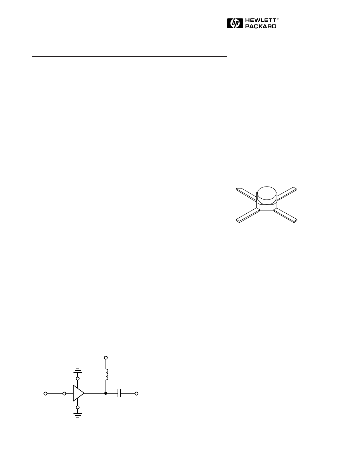
35 Micro-X Package
Typical Biasing Configuration
V
d
RFC
IN
5965-9005E
4
3
MGA
1
2
C
block
OUT
6-192
Page 2
MGA-64135 Absolute Maximum Ratings
Absolute
Symbol Parameter Units Maximum
V
d
P
diss
P
in
T
ch
T
STG
Device Voltage V 12
Total Power Dissipation
[2]
mW 650
CW RF Input Power dBm +13
Channel Temperature °C 175
Storage Temperature
[3]
°C -65 to 175
[1]
Thermal Resistance: θjc = 150°C/W
Liquid Crystal Measurement: 1 µ m Spot Size
[4]
; T
[5]
= 150°C
CH
Notes:
1. Operation of this device above any one of these parameters may cause
permanent damage.
2. Derate linearly at 8.3 mW/° C for
> 103°C.
T
CASE
3. Storage above +150° C may tarnish the leads of this package making it
difficult to solder into a circuit. After a device has been soldered into a
circuit, it may be safely stored up to 175°C.
4. The thermal resistance value is based on measurements taken with the
device soldered to a 25 mil Teflon PCB.
5. The small spot size of this technique results in a higher, though more
accurate determination of θ
than do alternate methods. See MEASURE-
jc
MENTS section for more information.
MGA-64135 Electrical Specifications, T
Symbol Parameters and Test Conditions: Vd = 10 V, Z
G
P
∆G
—
VSWR
P
1 dB
Power Gain (|S21|2) f = 2 to 6 G Hz dB 10.0 12.0
Gain Flatness f = 2 to 6 GHz dB ± 1.20
P
Gain Variation vs. Temperature f = 2 to 6 GHz dB ±0.5
T
= –25°C to +85° C
CASE
Input VSWR f = 2 to 6 GHz 1.5:1 2.0:1
Output VSWR f = 2 to 6 GHz 1.4:1 2.0:1
Output Power at 1 dB Gain Compression f = 2 to 6 GHz dBm 10.0 12.0
= 25° C
A
= 50 Ω Units Min. Typ. Max.
O
NF 50 Ω Noise Figure f = 2 to 6 GHz dB 7.5
— Reverse Isolation (|S21|2) f = 2 to 6 GHz dB 35
I
d
Device Current mA 35 50 65
6-193
Page 3

MGA-64135 Typical Performance, T
= 25° C
A
16
14
12
(dB)
P
G
10
8
6
0 6.0 8.02.0 4.0 10.0 0 4.0 6.02.0 8.0
FREQUENCY (GHz) FREQUENCY (GHz)
Figure 1. Power Gain vs. Frequency,
V
= 10 V.
d
2.0:1
1.8:1
1.6:1
VSWR
1.4:1
1.2:1
INPUT
OUTPUT
15
14
(dBm)
13
1 dB
P
12
11
Figure 2. Output Power @ 1 dB Gain
Compression vs. Frequency, V
= 10 V.
d
9.0
8.5
(dB)
8.0
NOISE FIGURE
7.5
7.0
2.0 6.04.0 8.0
FREQUENCY (GHz)
Figure 3. Noise Figure vs. Frequency,
= 10 V.
V
d
1.0:1
0 6.0 8.02.0 4.0 10.0
FREQUENCY (GHz)
Figure 4. VSWR vs. Frequency, Vd = 10 V.
MGA-64135 Typical Scattering Parameters (Z
Freq.
S
11
S
21
= 50 Ω, TA = 25° C, V
O
S
12
= 10 V)
d
S
GHz Mag Ang dB Mag Ang dB Mag Ang Mag Ang
0.5 .27 –38 10.6 3.38 174 –31.0 .028 –13 .38 –41
1.0 .18 –44 12.9 4.42 –9 –33.1 .022 –20 .26 –48
2.0 .14 –67 14.3 5.21 –54 –34.9 .018 –19 .16 –59
3.0 .17 –91 14.5 5.33 –93 –37.1 .014 –21 .11 –75
4.0 .20 –105 14.2 5.11 –131 –37.8 .013 –15 .11 –71
5.0 .18 –114 13.6 4.79 –167 –37.3 .014 –10 .14 –57
6.0 .07 –162 12.8 4.35 157 –38.5 .012 –1 .17 –41
7.0 .15 96 11.8 3.89 123 –36.0 .016 3 .16 –42
8.0 .23 76 10.8 3.46 92 –34.3 .019 4 .10 –54
9.0 .32 63 9.5 2.98 63 –29.3 .034 12 .04 159
10.0 .43 52 8.6 2.68 38 –27.6 .041 –11 .09 116
22
6-194
Page 4

35 Micro-X Package Dimensions
4
.085
2.15
GROUND
.083
2.11
DIA.
.057 ± .010
1.45 ± .25
.022
.56
RF INPUT
13
2
.100
2.54
.455 ± .030
11.54 ± .75
641
GROUND
RF OUTPUT
.020
.508
Notes:
(unless otherwise specified)
1. Dimensions are
2. Tolerances
in .xxx = ± 0.005
mm .xx = ± 0.13
.006 ± .002
.15 ± .05
mm
in
6-195
 Loading...