

Datasheet MF32M1-J9CATXX, MF365A-J9CATXX, MF3513-J9CATXX, MF34M1-J9CATXX, MF3257-J9CATXX Datasheet (Mitsubishi)
...Page 1
MITSUBISHI MEMORY CARD
STATIC RAM CARDS
8/16-bit Data Bus
Static RAM Card
Connector Type
Two- piece 68-pin
1. DESCRIPTION
Mitsubishi’s Static RAM cards provide large memory
capacities on a device approximately the size of a
credit card (85.6mm×54mm×3.3mm). The cards use
a 8/16 bit data-bus.
Available in 64KB, 128KB, 256KB, 512KB,
1 MB, 2 MB and 4 MB capacities, Mitsubishi’s
SRAM cards conform to the PC Card Standard.
Mitsubishi achieved high density memory, while
maintaining credit size by using a thin small outline
packaging technology (TSOP). The TSOP surpasses
conventional memory card chip-on-board packaging
technology where larger, surface-mount devices
result in a tradeoff between card size and optimum
memory density. The TSOP, with external leads
spaced on 20-mil centers, is over four times smaller
than standard equivalent pin count surface-mount
packages. This allows up to 8 memory ICs (plus
interface circuitry) to be mounted in a card that in
only 3.3mm thick.
MF365A-J9CATXX
MF3129-J9CATXX
MF3257-J9CATXX
MF3513-J9CATXX
MF31M1-J9CATXX
MF32M1-J9CATXX
MF34M1-J9CATXX
2. FEATURES
nUses TSOP (Thin Small Outline Package) to
achieve very high memory density coupled with
high reliability, without enlarging card size
nElectrostatic discharge protection to 15kV
nBuffered interface
nWrite protect switch
n68pin
nBuilt-in auxiliary battery
3. APPLICATIONS
nOffice automation nData Communication
nComputers nIndustrial
nTelecommunications nConsumer
4. PRODUCT LIST
Item Memory Data Bus Attribute Auxiliary
Type name capacity width(bits) memory battery
MF365A-J9CATXX 64KB
MF3129-J9CATXX 128KB
MF3257-J9CATXX 256KB
MF3513-J9CATXX 512KB 8/16 NO YES
MF31M1-J9CATXX 1MB
MF32M1-J9CATXX 2MB
MF34M1-J9CATXX 4MB
MITSUBISHI
ELECTRIC
1/14 Apr. 1999 Rev. 1.1
Page 2

MITSUBISHI MEMORY CARD
STATIC RAM CARDS
5. SUMMARY
MF3XXX-J9CATXX series is the Static RAM cards which has 8/16 bit changeable data-bus width.
The card has a replaceable lithium main battery to maintain data in memory and has an auxiliary battery to
maintain data in memory while the main battery is replaced. When the card is not use or the supply voltage
drops, the main battery will automatically maintain data in memory.
6. FUNCTIONAL DESCRIPTION
The function of the card is determined by the combination of the following five control signals,
REG#, CE1#, CE2#, OE#, WE#; active low signals. (Please refer to section 10 FUNCTION TABLE on page 5)
((1))COMMON MEMORY FUNCTION
When REG# signal is high level, the common memory area is selected.
((a))READ MODE
To read, WE# is set high level and CE1# or CE2# is set low level and the memory address is applied at inputs
A0-A21(4MB). Setting OE# low level executes the reading with output at data-bus. It is available to make the
following functions according to the combination of CE1# and CE2#.
When CE1# is set low level and CE2# is set high level, the card operates as an 8 bit data-bus width card.
The data can be dealt with lower data-bus(D0-D7).
When both CE1# and CE2# are set low level, the card operates as a 16 bit data-bus width card.
At this mode LSB of address-bus (A0) is ignored.
In addition odd byte can be accessed through upper data-bus(D8-D15) when CE1# is set high level and CE2# is
set low level. This mode is useful when handling only odd bytes in the 16 bit data-bus interface system (A0 is
ignored).
When both CE1# and CE2# are set high level, the card becomes a standby mode where the card consumes
low power and the data-bus is placed in high impedance state (above functions of CE1# and CE2# are the same
as in the following modes).
When both OE# and WE# are set high level, the card becomes a output disable mode and the data-bus is
placed in high impedance state.
((b))WRITE MODE
To write, the memory address is first applied at inputs A0-A21(4MB) and the data is applied at output pins.
Setting CE1# or CE2# low level, WE# low level and OE# high level executes the writing.
((2))ATTRIBUTE MEMORY FUNCTION
When REG# is set low level, the attribute memory area is selected. MF3XXX-J9CATXX series have no
attribute memory but outputs FFh on the lower data-bus(D0-D7) when the following conditions are applied
(a)setting CE1# low, CE2# high, OE# low, WE# high and A0 low
(b)setting CE1# low, CE2# low, OE# low and WE# high
((3))BATTERY
When the card is used for long periods of time, eventually battery exhaustion occurs. If such a situation is
encountered, replace any exhausted battery with a new one as directed in section 21.2 ″REPLACING BATTERY″
(page 14).
The replacement battery model number is indicated under section 21 ″BATTERY SPECIFICATIONS″(page 14).
7. WRITE PROTECT MODE
When the write protect switch is switched on, this card goes into a write protect mode that can read but not
write data. In this mode, WP pin becomes “H” level.
At the shipment the write protect switch is switched off (Normal mode : The card can be written ; WP pin
indicates “L” level).
MITSUBISHI
ELECTRIC
2/14 Apr. 1999 Rev. 1.1
Page 3
MITSUBISHI MEMORY CARD
1
GND
Ground
35
GND
Ground
A17 (NC for < 128KB types)
A18 (NC for < 256KB types)
A19 (NC for < 512KB types) Address
A20 (NC for < 1MB type) input
A21 (NC for < 2MB type)
STATIC RAM CARDS
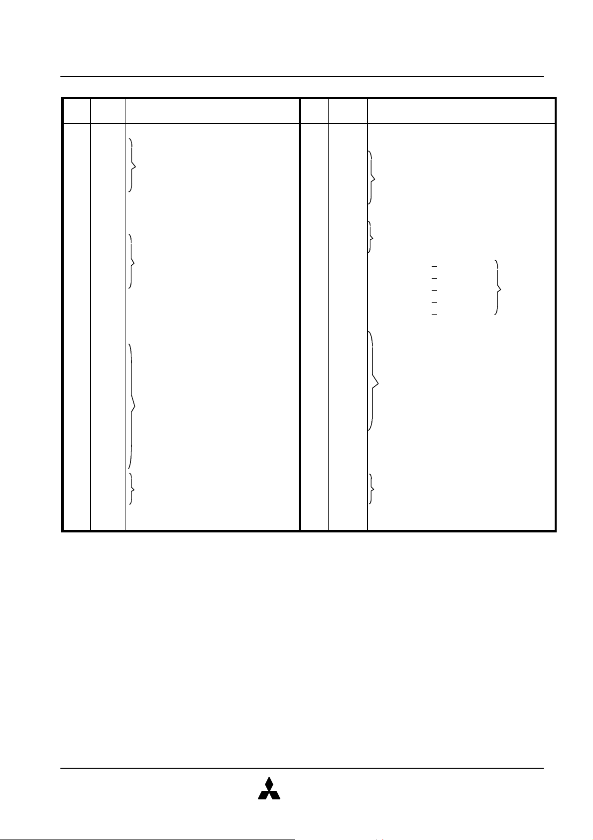
8. PIN ASSIGNMENTS
Pin Pin
Symbol
No. No.
Function
Symbol
Function
2 D3 36 CD1# Card detect 1
3 D4 37 D11
4 D5 Data I/O 38 D12
5 D6 39 D13 Data I/O
6 D7 40 D14
7 CE1# Card enable 1 41 D15
8 A10 Address input 42 CE2# Card enable 2
9 OE# Output enable 43 NC
10 A11 44 NC No connection
11 A9 45 NC
12 A8 Address input 46 A17
13 A13 47 A18
14 A14 48 A19
15 WE# Write enable 49 A20
16 NC No connection 50 A21
17 VCC Power supply voltage 51 VCC Power supply voltage
18 NC No connection 52 NC
19 A16 A16 (NC for 64KB type) 53 NC
20 A15 54 NC
21 A12 55 NC
22 A7 56 NC No connection
23 A6 57 NC
24 A5 Address input 58 NC
25 A4 59 NC
26 A3 60 NC
27 A2 61 REG# Attribute memory select
28 A1 62 BVD2 Battery voltage detect 2
29 A0 63 BVD1 Battery voltage detect 1
30 D0 64 D8
31 D1 Data I/O 65 D9 Data I/O
32 D2 66 D10
33 WP Write protect 67 CD2# Card detect 2
34 GND Ground 68 GND Ground
MITSUBISHI
ELECTRIC
3/14 Apr. 1999 Rev. 1.1
Page 4
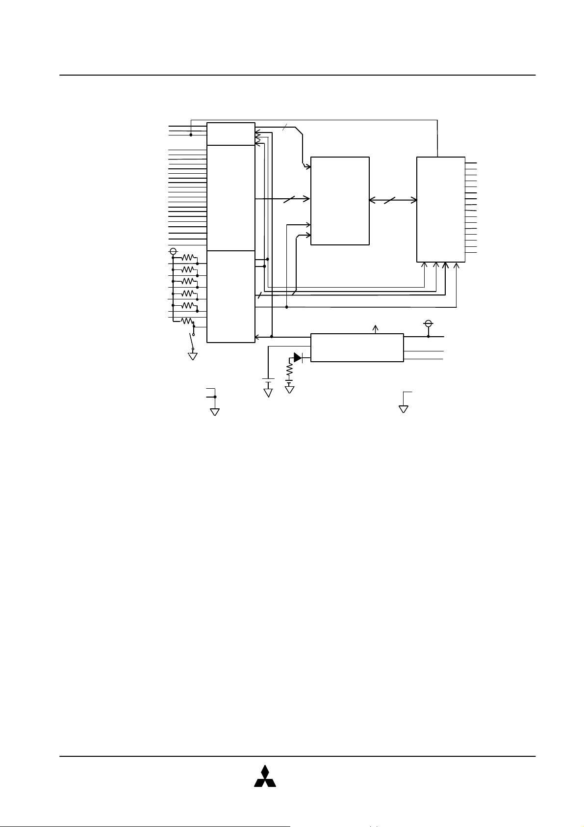
9. BLOCK DIAGRAM (4MB) (MF34M1-J9CATXX)
A21
WP#
WRITE PROTECT
ON
19
16
POWER CONTROLLER
DECODER
CR2025
2
MITSUBISHI MEMORY CARD
STATIC RAM CARDS
CE1#
CE2#
WE#
OE#
REG#
A20
A0
A19
A18
A17
A16
A15
A14
A13
A12
A11
A10
A9
A8
A7
A6
A5
A4
A3
A2
A1
OFF
CD1#
CD2#
ADDRESS-
ADDRESS-
BUS
BUFFERS
MODE
CONTROL
LOGIC
Auxiliary
battery
8
D15
CS#
COMMON
MEMORY
4Mbit SRAM×8
OE#
WE#
TO INTERNAL
POWER SUPPLY
VOLTAGE DETECTOR
&
DATA-BUS
BUFFERS
VCC
BVD2
D14
D13
D12
D11
D10
D9
D8
D7
D6
D5
D4
D3
D2
D1
D0
BVD1
GND
MITSUBISHI
ELECTRIC
4/14 Apr. 1999 Rev. 1.1
Page 5
MITSUBISHI MEMORY CARD
STATIC RAM CARDS
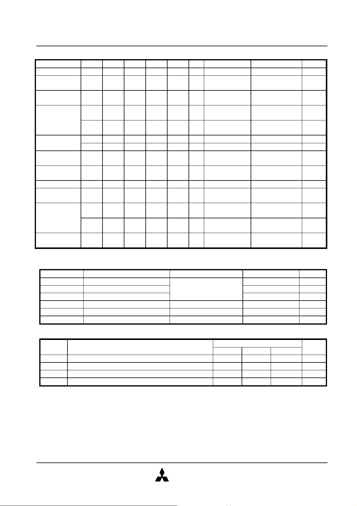
10. FUNCTION TABLE
Mode REG# CE1# CE2# OE# WE# A0 I/O (D15~D8) I/O (D7~D0) Icc
Standby X H H X X X High-impedance High-impedance standby
Read A (16bit)
common
Write A (16bit)
common
Read B (8bit)
common
H L L L H X Odd Byte
Data out
H L L H L X Odd Byte
Data in
Even Byte
Data out
Even Byte
Data in
H L H L H L High-impedance Even Byte
Data out
H L H L H H High-impedance Odd Byte
Active
Active
Active
Active
Data out
Write B (8bit)
H L H H L L High-impedance Even Byte Data in Active
common H L H H L H High-impedance Odd Byte Data in Active
Read C (8bit)
common
Write C (8bit)
common
H H L L H X Odd Byte
Data out
H H L H L X Odd Byte
Data in
High-impedance Active
High-impedance Active
Output disable X X X H H X High-impedance High-impedance Active
Read A (16bit)
attribute
Read B (8bit)
attribute
L L L L H X Data out
(unknown)
Data out
(FFh)
L L H L H L High-impedance Data out
(FFh)
L L H L H H High-impedance Data out
Active
Active
Active
(unknown)
Read C (8bit)
attribute
Note 1 : H=VIH, L=VIL, X=VIH or VIL
L H L L H X Data out
(unknown)
High-impedance Active
11. ABSOLUTE MAXIMUM RATINGS
Symbol Parameter Conditions Ratings Unit
Vcc Supply voltage -0.3~6.0 V
VI Input voltage With respect to GND -0.3~VCC+0.3 V
VO Output voltage 0~VCC V
Topr1 Operating temperature 1 Read, Write Operation 0~60 °C
Topr2 Operating temperature 2 Data retention 0~60 °C
Tstg Storage temperature Excludes data retention -20~70 °C
12. RECOMMENDED OPERATING CONDITIONS (Ta=0~55°C, unless otherwise noted)
Symbol
Parameter
Min. Typ. Max.
Limits
Unit
Vcc Vcc Supply voltage 4.75 5.0 5.25 V
GND System ground 0 V
VIH High input voltage 2.4 VCC V
VIL Low input voltage 0 0.8 V
MITSUBISHI
ELECTRIC
5/14 Apr. 1999 Rev. 1.1
Page 6

MITSUBISHI MEMORY CARD
STATIC RAM CARDS
13. ELECTRICAL CHARACTERISTICS (Ta=0~55°C, Vcc=5V±5%, unless otherwise noted)
Symbol Parameter Test conditions Limits Unit
Min. Typ. Max.
VOH High output voltage IOH= -1.0mA 2.4 V
VOL Low output voltage IOL=2mA 0.4 V
IIH High input current VI=Vcc V 10 µA
IIL Low input current VI=0V CE1#, CE2#, WE#, OE#, REG# -10 -70 µA
Other inputs -10
IOZH High output current CE1#=CE2#=VIH or OE#=VIH WE#=VIH, 10 µA
in off state VO=Vcc
IOZL Low output current CE1#=CE2#=VIH or OE#=VIH WE#=VIH, -10 µA
in off state VO=0V
Icc 1 • 1 Active supply CE1#=CE2#=VIL, other inputs 64KB~512KB 170 mA
current 1 =VIH or VIL,Outputs=open 1MB~4MB 230
Icc 1 • 2 Active supply
current 2
CE1#=CE2# ≤ 0.2V, other
inputs ≤ 0.2V or
≥ Vcc-0.2V, Outputs=open
64KB~512KB 160 mA
1MB~4MB 220
Icc 2 • 1 Standby supply CE1#=CE2#=VIH 64KB~4MB 10 mA
current 1 other inputs=VIH or VIL (17)
Icc 2 • 2 Standby supply
current 2
CE1#=CE2# ≥ Vcc-0.2V
other inputs ≤ 0.2V or
≥ Vcc-0.2V
64KB~512KB 0.45
(7.45)
1MB~4MB 0.65
mA
(7.65)
VBDET1 Battery detect Vcc=5V, Ta=25°C 2.27 2.37 2.47 V
reference voltage
VBDET2 Battery detect Vcc=5V, Ta=25°C 2.55 2.65 2.75 V
reference voltage
Note 2 : Currents flowing into the card are taken as positive (unsigned).
3 : Typical values are measured at Vcc=5V, Ta=25°C.
4 : The figure in the parentheses indicates the standby current limits when the built-in auxiliary battery is
not fully charged.
14. CAPACITANCE
Symbol
CI
CO
Parameter
Input capacitance VI=GND, vi=25mVrms
f=1MHZ, Ta=25°C 30 pF
Output Capacitance
Vo=GND, vo=25mVrms
f=1MHz, Ta=25°C
Note 4 : These parameters are not 100% tested.
Test conditions
Limits
Min. Typ. Max.
20 pF
Unit
MITSUBISHI
ELECTRIC
6/14 Apr. 1999 Rev. 1.1
Page 7

MITSUBISHI MEMORY CARD
STATIC RAM CARDS
15. SWITCHING CHARACTERISTICS
Read Cycle (Ta=0~55°C, VCC=5V±5%, unless otherwise noted)
Symbol Parameter Limits Unit
Min. Max.
tcR Read cycle time 150 ns
ta(A) Address access time 150 ns
ta(CE) Card enable access time 150 ns
ta(OE) Output enable access time 75 ns
tdis(CE) Output disable time (from CE#) 75 ns
tdis(OE) Output disable time (from OE#) 75 ns
ten(CE) Output enable time (from CE#) 5 ns
ten(OE) Output enable time (from OE#) 5 ns
tV(A) Data valid time (after address change) 0 ns
16. TIMING REQUIREMENTS
Write Cycle (Ta=0~55°C, Vcc=5V±5%, unless otherwise noted)
Symbol Parameter Limits Unit
Min. Max.
tcW Write cycle time 150 ns
tw(WE) Write pulse width 80 ns
tsu(A) Address set up time 20 ns
tsu(A-WEH) Address set up time with respect to WE# high 100 ns
tsu(CE-WEH) Card enable set up time with respect to WE# high 100 ns
t(D-WEH) Data set up time with respect to WE# high 50 ns
th(D) Data hold time 20 ns
trec(WE) Write recovery time 20 ns
tdis(WE) Output disable time (from WE#) 75 ns
tdis(OE) Output disable time (from OE#) 75 ns
ten(WE) Output enable time (from WE#) 5 ns
ten(OE) Output enable time (from OE#) 5 ns
tsu(OE-WE) OE# set up time with respect to WE# low 10 ns
th(OE-WE) OE# hold time with respect to WE# high 10 ns
MITSUBISHI
ELECTRIC
7/14 Apr. 1999 Rev. 1.1
Page 8

TIMING DIAGRAM
Hi-Z
tSU(A-WEH)
tSU(A)
th(OE-WE)
Hi-Z
tcR
ta(CE)
ten(CE)
ten(OE)
tdis(OE)
tV(A)
tdis(CE)
Read Cycle
MITSUBISHI MEMORY CARD
STATIC RAM CARDS
An
VIH
VIL
VIH
CE#
VIL
VIH
OE#
VIL
Dm
(DOUT)
Write Cycle (WE# control)
VOH
VOL
WE#=“H” level
REG#=“H” level
VIH
An
VIL
ta(A)
ta(OE)
Hi-Z
OUTPUT VALID
tCW
CE#
OE#
WE#
Dm
(DIN)
Dm
(DOUT)
VIH
VIL
VIH
VIL
VIH
VIL
VIH
VIL
VOH
VOL
REG#=“H” level
tSU(OE-WE)
tdis(OE)
tSU(CE-WEH)
tW(WE)
t(D-WEH)
DATA INPUT STABLE
tdis(WE)
trec(WE)
th(D)
ten(OE)
ten(WE)
MITSUBISHI
ELECTRIC
8/14 Apr. 1999 Rev. 1.1
Page 9

Write Cycle (CE# control)
tCW
tSU(CE-WEH)
tSU(A)
th(D)
Hi-Z
VIH
An
VIL
VIH
CE#
VIL
VIH
WE#
VIL
Dm
(DIN)
VIH
VIL
MITSUBISHI MEMORY CARD
STATIC RAM CARDS
trec(WE)
t(D-WEH)
DATA INPUT STABLE
OE#=“H” level
REG#=“H” level
17. SWITCHING CHARACTERISTICS (Attribute)
Read Cycle (Ta=0~55°C, Vcc=5V±5%, unless otherwise noted)
Symbol Parameter Limits Unit
Min. Max.
tcRR Read cycle time 300 ns
ta(A)R Address access time 300 ns
ta(CE)R Card enable access time 300 ns
ta(OE)R Output enable access time 150 ns
tdis(CE)R Output disable time (from CE#) 100 ns
tdis(OE)R Output disable time (from OE#) 100 ns
ten(CE)R Output enable time (from CE#) 5 ns
ten(OE)R Output enable time (from OE#) 5 ns
tV(A)R Data valid time after address change 0 ns
MITSUBISHI
ELECTRIC
9/14 Apr. 1999 Rev. 1.1
Page 10

TIMING DIAGRAM (Attribute)
tcRR
ta(CE)R
ten(CE)R
ten(OE)R
tdis(OE)R
tV(A)R
OUTPUT VALID
Hi-Z
tdis(CE)R
Read Cycle
An
VIH
VIL
VIH
CE#
VIL
MITSUBISHI MEMORY CARD
STATIC RAM CARDS
ta(A)R
VIH
ta(OE)R
OE#
VIL
Dm
(DOUT)
VOH
VOL
WE#=“H” level
REG#=“L” level
Note 5 : Test Conditions
Input pulse levels : VIL=0.4V, VIH=2.8V
Input pulse rise, fall time : tr=tf=10ns
Reference voltage
Input : VIL=0.8V, VIH=2.4V
Output : VOL=0.8V, VOH=2.0V
(ten and tdis are measured when output voltage is ± 500mV from steady state. )
Load : 100pF + 1 TTL gate
5pF + 1 TTL gate (at ten and tdis measuring)
6 : Indicates the don’t care input
7 : Writing is executed in overlap of CE# and WE# are “L” level. (only for Common Memory)
8 : Don’t apply inverted phase signal externally when Dm pin is in output mode.
9 : CE# is indicated as follows:
Read A/Write A : CE#=CE1#=CE2#
Read B/Write B : CE#=CE1#, CE2#=“H” level
Read C/Write C : CE#=CE2#, CE1#=“H” level
MITSUBISHI
ELECTRIC
10/14 Apr. 1999 Rev. 1.1
Page 11

MITSUBISHI MEMORY CARD
CE2#
CE2#
90%
STATIC RAM CARDS
18. ELECTRICAL CHARACTERISTICS
BATTERY BACKUP (Ta=0~55°C, unless otherwise noted)
Symbol Parameter Test conditions Limits Unit
Min. Typ. Max.
VBATT Back-up enable battery voltage All pins open 2.6 V
Vi(CE)
Card enable voltage
2.4V≤VCC≤5.25V
0V≤VCC<2.4V
2.4 V
Vcc-0.1 Vcc Vcc+0.1
64KB 3
128KB 3
All pins open, 256KB 3
Battery back-up supply current VBATT=3V, 512KB 5
µA
Ta=25°C 1MB 3
2MB 5
Icc 4MB 9
(Bup)
64KB 30
128KB 30
All pins open, 256KB 30
Battery back-up supply current VBATT=3V 512KB 50
µA
1MB 30
2MB 50
4MB 90
19. TIMING REQUIREMENTS (Ta=0~55°C, unless otherwise noted)
Symbol Parameter Limits Unit
Min. Typ. Max.
Tpr Power supply rise time 0.1 300 ms
tpf Power supply fall time 3 300 ms
tsu(Vcc) Setup time at power on 20 ms
trec(Vcc) Recovery time at power off 1000 ns
CARD INSERTION/REMOVAL TIMING DIAGRAM
VCC
CE1#,
tpf
VCC MIN VCC MIN
trec(VCC)
90%
VIH
10%
10%
VIH
tpr
VCC
tsu(VCC)
CE1#,
20. BATTERY SPECIFICATIONS
Please use the following coin type lithium battery.
Type of main battery; CR2025 or equivalents
20.1 BATTERY LIFE EXPECTANCY
The calculated main battery’s life expectancies are as follows.
Card Type main battery’s life
(when the card is left continuously)
MF365A-J9CATXX 5.9years
MF3129-J9CATXX 5.9years
MF3257-J9CATXX 5.9years
MF3513-J9CATXX 3.6years
MF31M1-J9CATXX 5.9years
MF32M1-J9CATXX 3.6years
MF34M1-J9CATXX 2.0years
Conditions; Temperature : 25°C Humidity : 60%RH
MITSUBISHI
ELECTRIC
11/14 Apr. 1999 Rev. 1.1
Page 12

MITSUBISHI MEMORY CARD
STATIC RAM CARDS
20.2 REPLACING BATTERY
MF3XXX-J9CATXX series have two batteries inside the card as follows.
Lithium battery; for main battery (replaceable)
Rechargeable battery; for auxiliary battery (not replaceable)
For main battery replacement, perform the following procedure. Performing any other procedures will lose the
data recorded in the IC card.
(1)Have on hand a new main battery that has the same model number as or is equivalent currently installed one.
(2)Insert the IC card into the system and apply power to the IC card so that the auxiliary battery will be charged.
(more than 5 minutes)
(3)While pressing the main battery holder cam release levers inward, slowly withdraw the main battery holder.
(4)With the new main battery set in the battery holder, insert it completely into the IC card.
(5)If the battery holder is incorrectly oriented, it will not smoothly fit into its position or the IC card will bulge.
If such a situation is encountered, properly reorient the battery and battery holder and try again.
(6)Insert the battery holder until it clicks into position.
<NOTICE>
Main battery replacement must be completed quickly (recommended time is within 10 minutes).
If too much time is taken, the recorded data may be lost.
The built-in auxiliary battery cannot be replaced.
21. CONNECTOR
The number of card insertion and removal are as follows.
Office environment 10000 times min. at speed of 10 cycles/min.
Harsh environment 5000 times min. at speed of 10 cycles/min.
22. CARD WEIGHT about 35g
23. UL CLASS OF MAIN CARD PARTS
(1)MAIN FRAME UL94V-0
(2)PCB UL94V-0
(3)PLASTIC PART OF CONNECTOR UL94V-0
24. THE BATTERY VOLTAGE DETECT SIGNALS ((BVD1,2))
BVD1 BVD2 Comment
H H Battery operational
H L Battery operational, but battery should be replaced
L L Battery and data integrity is not kept
Note10. The battery voltage detect signals indicate the present state of the battery.
They do not guarantee the data retention.
25.CONCERNING THE SECURITY OF DATA
There is always the possibility that a soft-error (this malfunction is not permanent hence it is called soft and
the data can be restored by rewriting) may occur with semiconductor products.
When keeping the important data within an IC card, remember to give due consideration to safety when
making your circuit designs, with appropriate measures such as
(1) Keeping multiple copies of the data.
(2) Addition of ECC or CRC by software or hardware.
MITSUBISHI
ELECTRIC
12/14 Apr. 1999 Rev. 1.1
Page 13

MITSUBISHI MEMORY CARD
STATIC RAM CARDS
! Warning ( if card with battery / card with auxiliary battery )
(1)Do not charge, short, disassemble, deform, heat, or throw the batteries into fire, as they may ignite, overheat,
rupture or explode.
(2)Place the batteries out of the reach of children. If somebody swallows them, they should see a doctor
immediately.
(3)When discarding or storing the batteries, wrap them individually with cellophane tape or other nonconductive
material. If they are positioned in contact with any other metals or batteries, they may explode, rupture or
leak electrolyte solution.
! Caution
This product is not designed or manufactured for use in a device or system that is used under circumstances in
which human life is potentially at stake. Please contact Mitsubishi Electric Corporation or an authorized
Mitsubishi Semiconductor product distributor when considering the use of a product contained herein for a
special applications, such as apparatus or systems for transportation, vehicular, medical, aerospace, nuclear,
or undersea repeater use.
Keep safety first in your circuit designs!
Mitsubishi Electric Corporation puts the maximum effort into making semiconductor products better and more
reliable, but there is always the possibility that trouble may occur with them. Trouble with semiconductors may
lead to personal injury, fire or property damage. Remember to give due consideration to safety when making
your circuit designs, with appropriate measures such as (1)placement of substitutive, auxiliary circuits,(2)use of
non-flammable material or (3)prevention against any malfunction or mishap.
Notes regarding these materials
lThese materials are intended as a reference to assist our customers in the selection of the Mitsubishi
semiconductor product best suited to the customer’s application; they do not convey any license under any
intellectual property rights, or any other rights, belonging to Mitsubishi Electric Corporation or a third party.
l Mitsubishi Electric Corporation assumes no responsibility for any damage, or infringement of any third party’s rights, originating in the use of any product data, diagrams, charts or circuit application examples
contained in these materials.
l All information contained in these materials, including product data, diagrams and charts, represent
information on products at the time of publication of these materials, and are subject to change by Mitsubishi
Electric Corporation without notice due to product improvements or other reasons. It is therefore
recommended that customers contact Mitsubishi Electric Corporation or an authorized Mitsubishi
Semiconductor product distributor for the latest product information before purchasing a product listed
herein.
l For instruction on proper use of the IC card, thoroughly read the manual attached to the product before use.
After reading please store the manual in s safe place for future reference.
l The prior written approval of Mitsubishi Electric Corporation is necessary to reprint or reproduce in whole
or in part these materials.
l If these products or technologies are subject the Japanese export control restrictions, they must be exported
under a license from the Japanese government and cannot be imported into a country other than approved
destination. Any diversion or re-export contrary to the export control laws and regulations of Japan and/or
the country of destination is prohibited.
l Please contact Mitsubishi Electric Corporation or an authorized Mitsubishi Semiconductor product
distributor for further details on these materials or the products contained therein.
MITSUBISHI
ELECTRIC
13/14 Apr. 1999 Rev. 1.1
Page 14

OUTLINE(68P-012)
MITSUBISHI MEMORY CARD
STATIC RAM CARDS
MITSUBISHI
ELECTRIC
14/14 Apr.1999 Rev.1.1
 Loading...