

Page 1

MDT2005
MDT2005
1. General Description
This EPROM-Based 8-bit micro-controller uses a fully static CMOS design technology
combines higher speeds and smaller size with the low power and high noise immunity of
CMOS.
On chip memory system includes 0.5 K(for MDT2005) bytes of ROM, and 32 bytes of static
RAM.
2. Features
The followings are some of the features on the hardware and software :
u Fully COMS static design
u 8-bit data bus
u On chip ROM size : 512 words for MDT2005
u Internal RAM size : 32 bytes
(25 general purpose registers, 7 special registers)
u 36 single word instructions
u 14-bit instructions
u 2-level stacks
u Operating voltage : 2.3V ~ 6.3 V
u Operating frequency : 0 ~ 20 MHz
u The most fast execution time is 200 ns under 20 MHz in all single cycle instructions except
the branch instruction
u Addressing modes include direct, indirect and relative addressing modes
u Power-on Reset
u Power edge-detector Reset
u Sleep Mode for power saving
u 8-bit real time clock/counter(RTCC) with 8-bit programmable prescaler
u 4 types of oscillator can be selected by programming option:
RC-Low cost RC oscillator
LFXT-Low frequency crystal oscillator
XTAL-Standard crystal oscillator
HFXT-High frequency crystal oscillator
u 4 oscillator start-up time can be selected by programming option:
150 µs, 20 ms, 40 ms, 80 ms
This specification are subject to be changed without notice. Any latest information please preview
http;//www.mdtic.com.tw P. 1 VER1.1
Page 2
MDT2005
u On-chip RC oscillator based Watchdog Timer(WDT) can be operated freely
u 12 I/O pins with their own independent direction control
3. Applications
The application areas of this MDT2005 range from appliance motor control and high speed
automot ive to low power remote transmitters/receivers, pointing devices, and
telecommunications processors, such as Remote controller, small instruments, chargers, toy,
automobile and PC peripheral … etc.
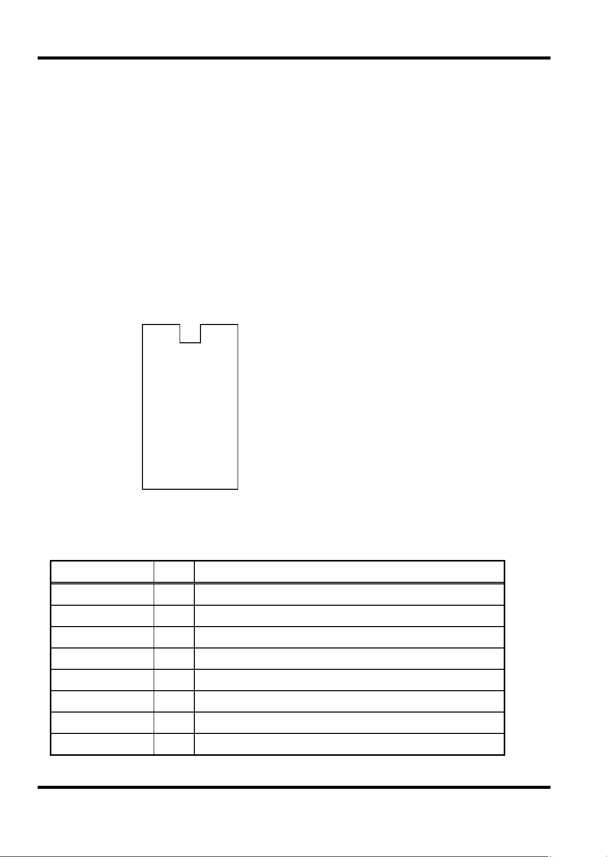
4. Pin Assignment
PA2 1 18 PA1
PA3 2 17 PA0
RTCC 3 16 OSC1
/MCLR 4 15 OSC2
Vss 5 14 Vdd
PB0 6 13 PB7
PB1 7 12 PB6
PB2 8 11 PB5
PB3 9 10 PB4
5. Pin Function Description
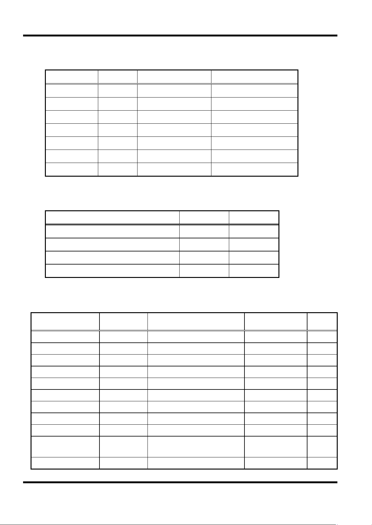
Pin Name I/O Function Description
PA0~PA3 I/O Port A, TTL input level
PB0~PB7 I/O Port B, TTL input level
RTCC I Real Time Clock/Counter, Schmitt Trigger input levels
/MCLR I Master Clear, Schmitt Trigger input levels
OSC1 I Oscillator Input
OSC2 O Oscillator Output
Vdd Power supply
Vss Ground
This specification are subject to be changed without notice. Any latest information please preview
http;//www.mdtic.com.tw P. 2 VER1.1
Page 3
6. Memory Map
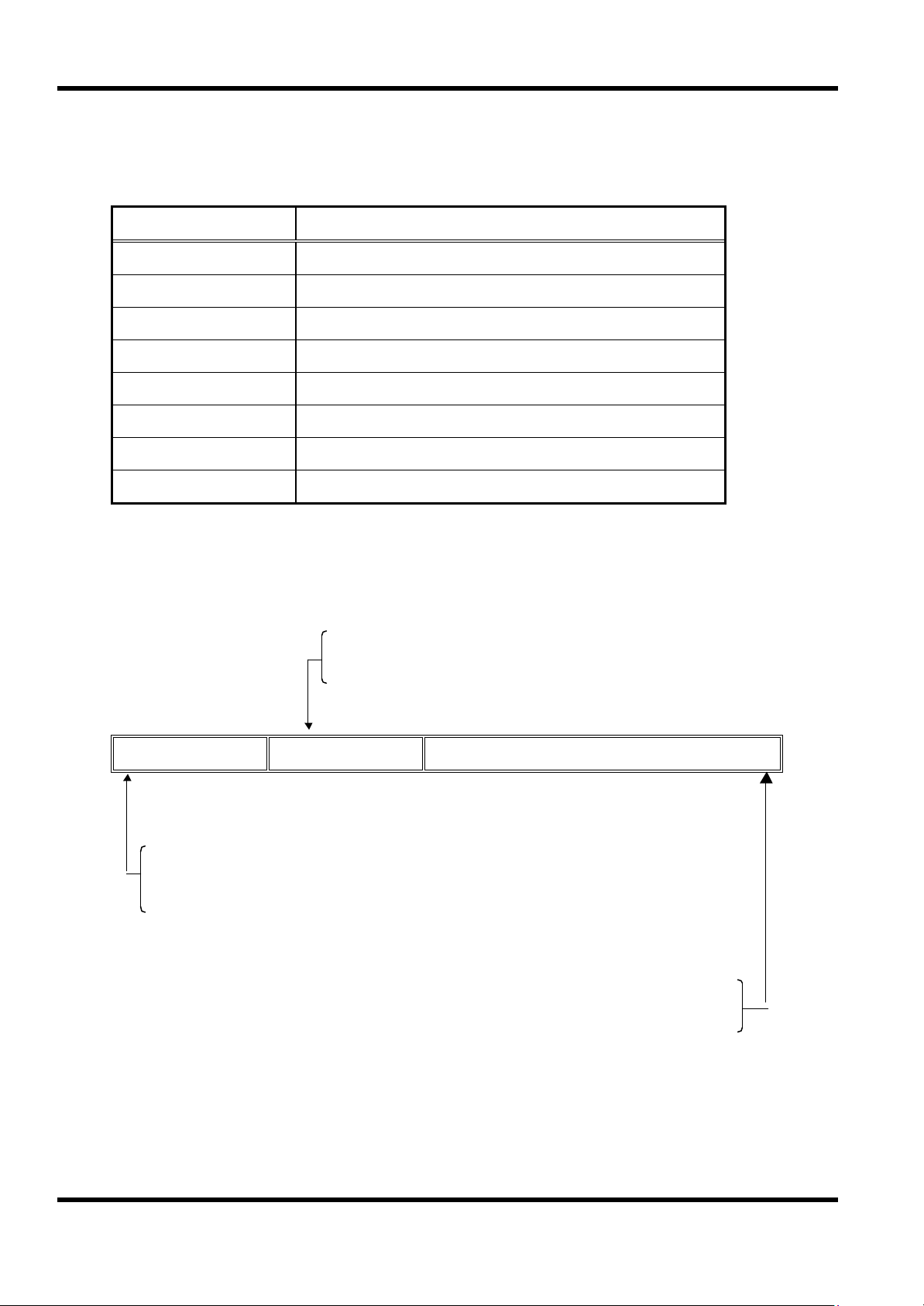
(A) Register Map
Address Description
00 Indirect Addressing Register
01 RTCC
02 PC
03 STATUS
04 MSR
05 Port A
06 Port B
07~1F Internal RAM, General Purpose Register
MDT2005
(1) IAR ( Indirect Address Register) : R0
(2) RTCC (Real Time Counter/Counter Register) : R1
(3) PC (Program Counter) : R2
Write PC, CALL --- always 0
LJUMP, JUMP, LCALL --- from instruction word
RTIW, RET --- from STACK
A9 A8 A7~A0
Write PC, JUMP, CALL --- always 0 (ROM 0.5K)
LJUMP, LCALL --- from instruction word
RTIW, RET --- from STACK
Write PC --- from ALU
LJUMP, JUMP, LCALL, CALL --- from instruction word
RTIW, RET --- from STACK
This specification are subject to be changed without notice. Any latest information please preview
http;//www.mdtic.com.tw P. 3 VER1.1
Page 4
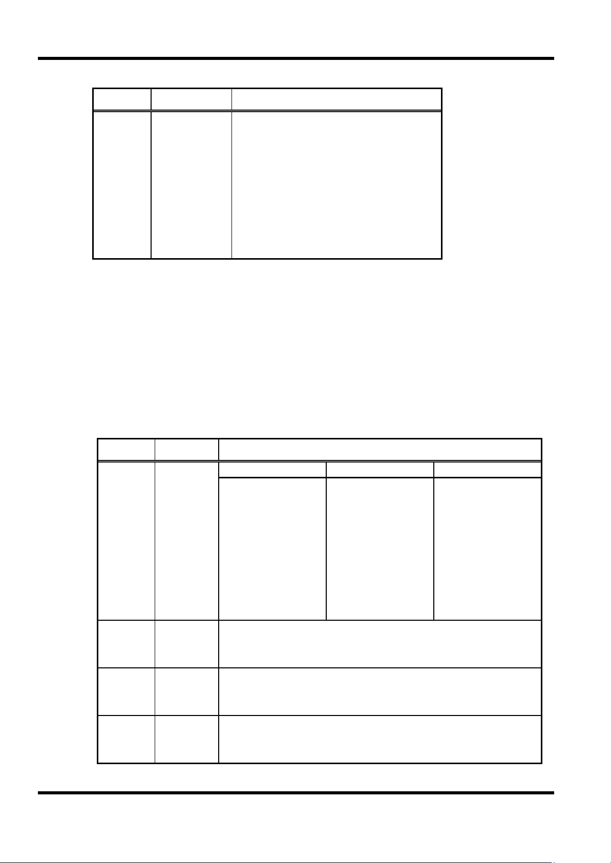
(4) STATUS (Status register) : R3
Bit Symbol Function
MDT2005
0
1
2
3
4
5-7
(5) MSR (Memory Select Register) : R4
(6) PORT A : R5
PA3~PA0, I/O Register
(7) PORT B : R6
(8) TMR (Time Mode Register)
C
HC
Z
PF
TF
——
PB7~PB0, I/O Register
Carry bit
Half Carry bit
Zero bit
Power loss Flag bit
Time overflow Flag bit
General purpose bit
Bit Symbol Function
Prescaler Value RTCC rate WDT rate
2—0
3
4
5
PS2—0
PSC
TCE
TCS
0 0 0
0 0 1
0 1 0
0 1 1
1 0 0
1 0 1
1 1 0
1 1 1
Prescaler assignment bit :
0 — RTCC
1 — Watchdog Timer
RTCC signal Edge :
0 — Increment on low-to-high transition on RTCC pin
1 — Increment on high-to-low transition on RTCC pin
RTCC signal set :
0 — Internal instruction cycle clock
1 — Transition on RTCC pin
1 : 2
1 : 4
1 : 8
1 : 16
1 : 32
1 : 64
1 : 128
1 : 256
1 : 1
1 : 2
1 : 4
1 : 8
1 : 16
1 : 32
1 : 64
1 : 128
This specification are subject to be changed without notice. Any latest information please preview
http;//www.mdtic.com.tw P. 4 VER1.1
Page 5
(9) CPIO A, CPIO B (Control Port I/O Mode Register)
The CPIO register is “write-only”
=“0”, I/O pin in output mode;
=“1”, I/O pin in input mode.
(10) EPROM Option by writer programming :
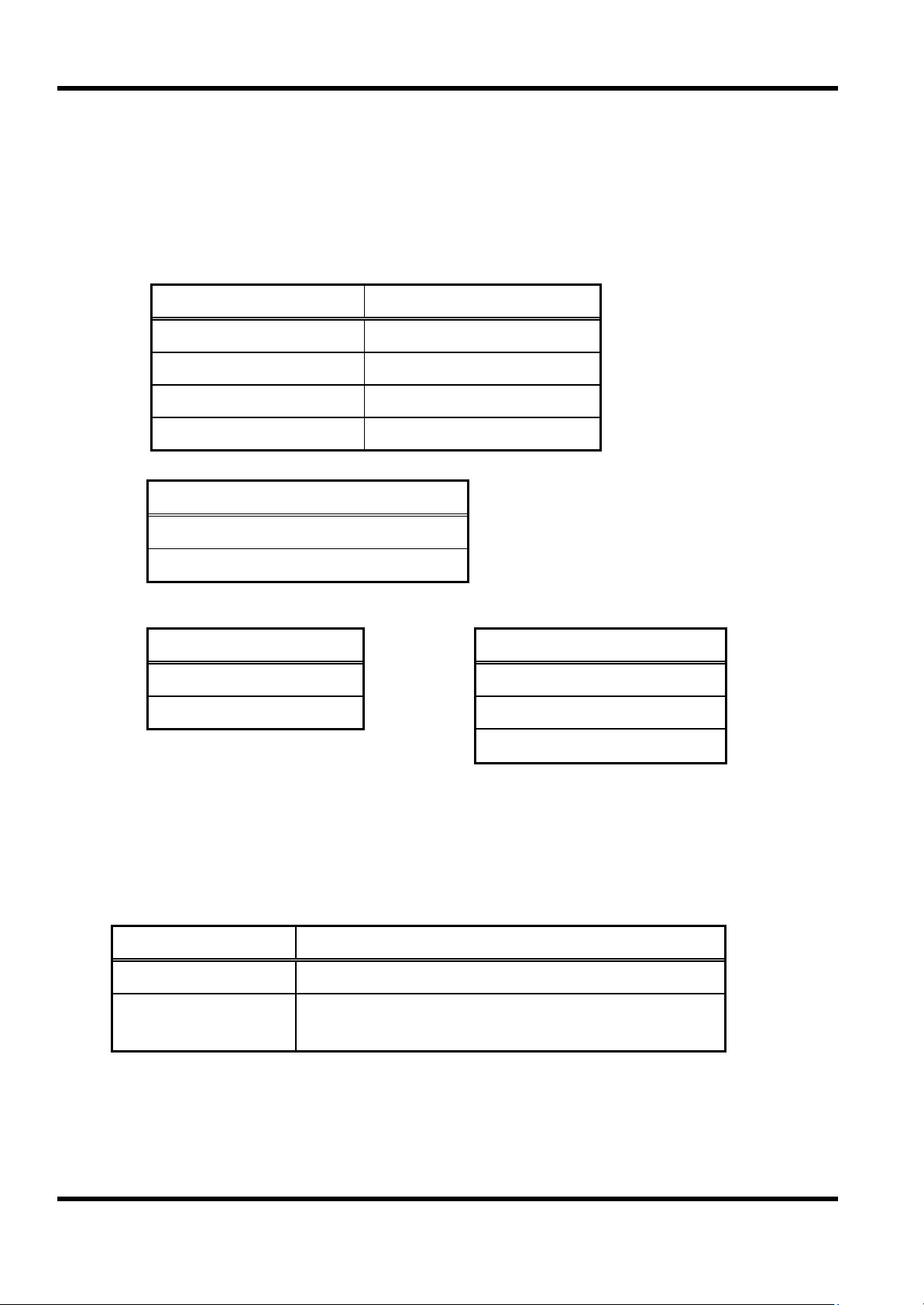
Oscillator Type Oscillator Start-up Time
MDT2005
RC Oscillator
HFXT Oscillator 20 ms,40ms,80ms
XTAL Oscillator 20ms,40 ms,80ms
LFXT Oscillator 40 ms,80 ms
Watchdog Timer control
Watchdog timer disable all the time
Watchdog timer enable all the time
Power Edge Detect Security bit
PED Disable Security weak Disable
PED Enable Security Disable
Security Enable
The default EPROM security is weak disable. Once the IC was set in enable or disable, it’s
forbidden to set in disable or enable again.
(B) Program Memory
150 µs,20ms,40ms,80ms
Address Description
000-1FF Program memory for MDT2005
1FF The starting address of the power on, external reset
or WDT for MDT2005
This specification are subject to be changed without notice. Any latest information please preview
http;//www.mdtic.com.tw P. 5 VER1.1
Page 6
eration
WT, stop OSC
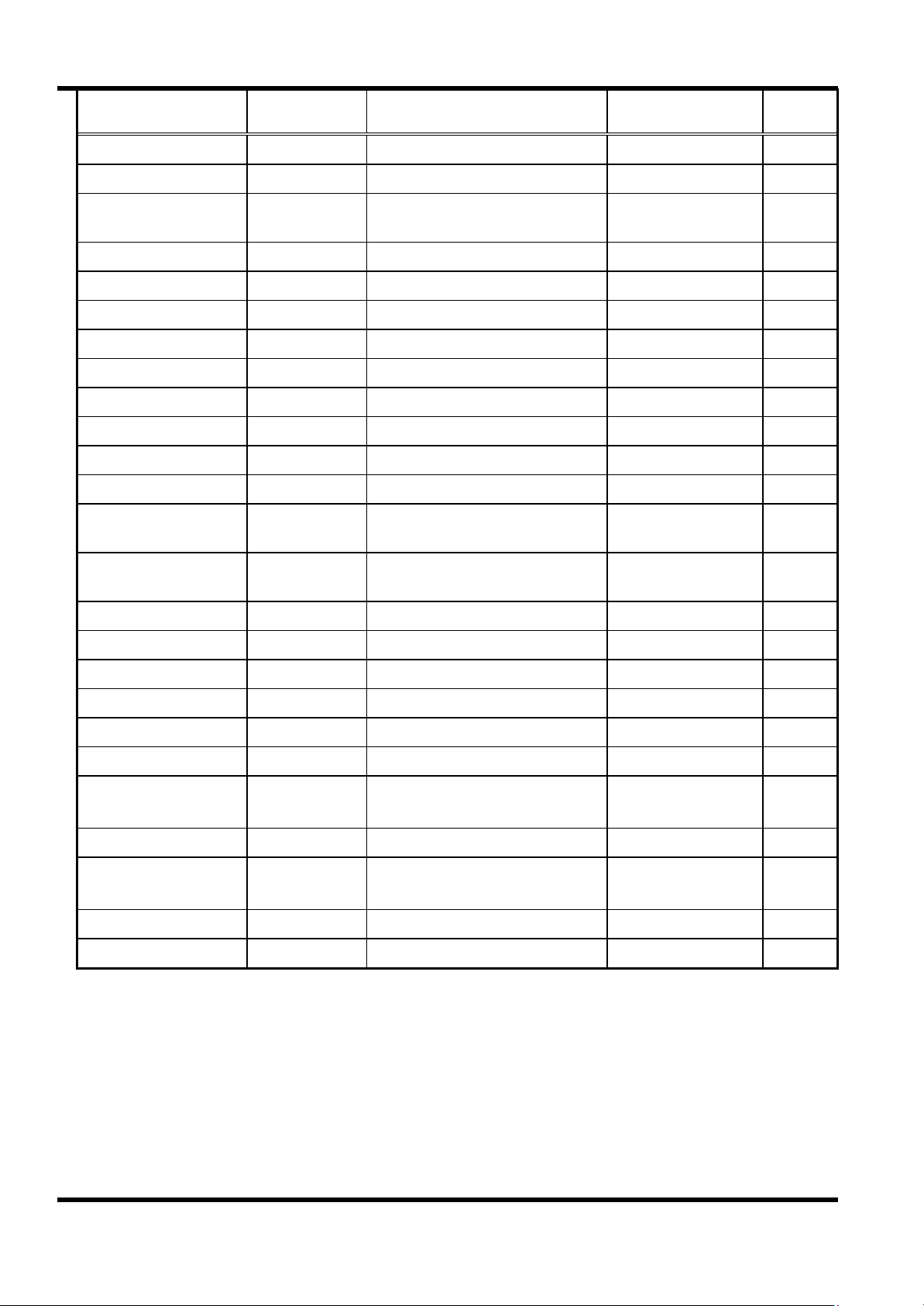
7. Reset Condition for all Registers
Register Address Power-On Reset /MCLR or WDT Reset
MDT2005
IAR 00h
- -
RTCC 01h xxxx xxxx uuuu uuuu
PC 02h 1111 1111 1111 1111
STATUS 03h 0001 1xxx 000# #uuu
MSR 04h 111x xxxx 111u uuuu
PORT A 05h - - - - xxxx - - - - uuuu
PORT B 06h xxxx xxxx uuuu uuuu
Note : u=unchanged, x=unknown, - =unimplemented, read as “0”
#=value depends on the condition of the following table
Condition Status: bit 4 Status: bit 3
/MCLR reset (not during SLEEP) u u
/MCLR reset during SLEEP 1 0
WDT reset (not during SLEEP) 0 1
WDT reset during SLEEP 0 0
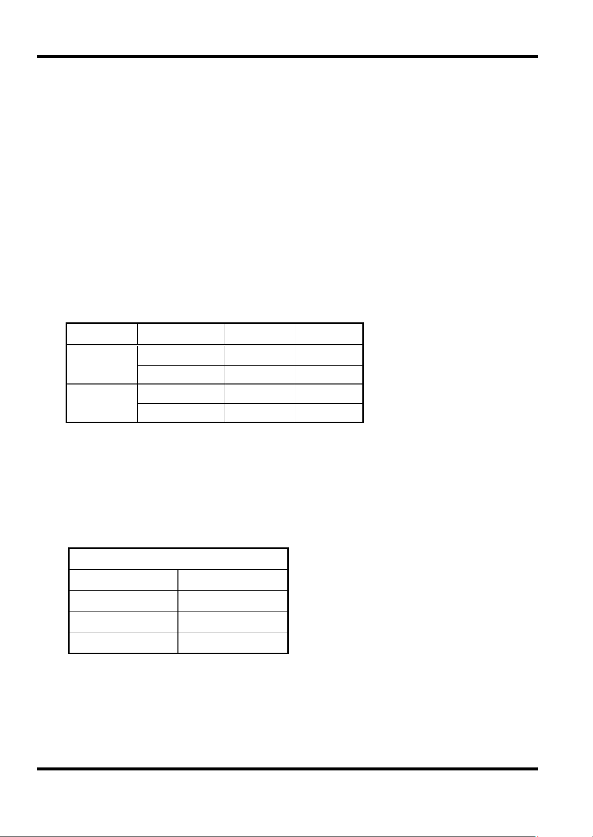
8. Instruction Set
Instruction Code
010000 00000000 NOP No op
010000 00000001 CLRWT Clear Watchdog timer 0→WT TF, PF
010000 00000010 SLEEP Sleep mode 0→
010000 00000011 TMODE Load W to TMODE register W→TMODE None
010000 00000100 RET Return Stack→PC None
010000 00000rrr CPIO R Control I/O port register W→CPIO r None
010001 1rrrrrrr STWR R Store W to register W→R None
011000 trrrrrrr LDR R, t Load register R→t Z
111010 iiiiiiii LDWI I Load immediate to W I →W None
010111 trrrrrrr SWAPR R, t Swap halves register
Mnemonic
Operands
Function Operating Status
None
TF, PF
[R(0~3) ↔
R(4~7)]→t
None
011001 trrrrrrr INCR R, t Increment register R + 1→t Z
This specification are subject to be changed without notice. Any latest information please preview
http;//www.mdtic.com.tw P. 6 VER1.1
Page 7
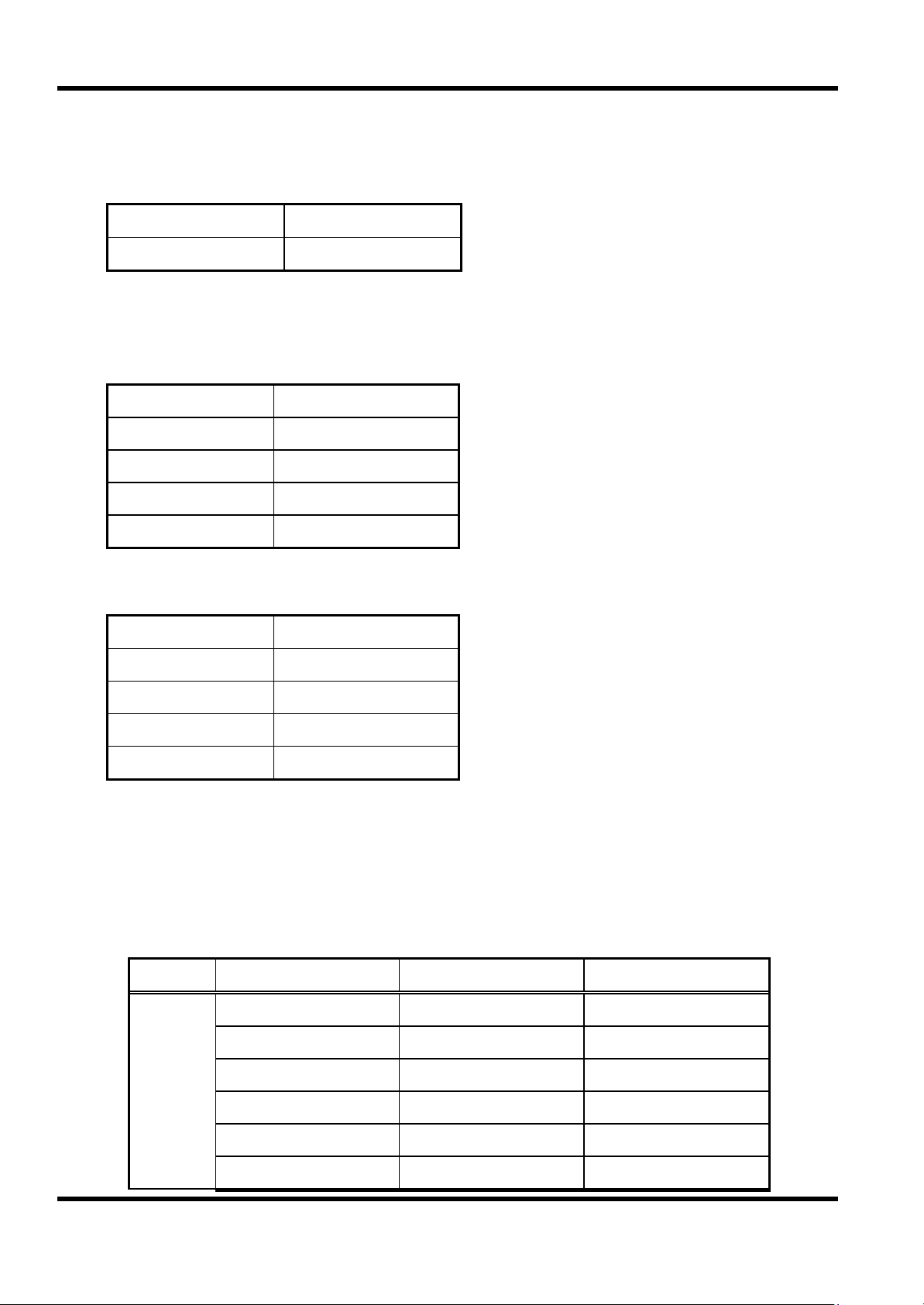
MDT2005
Complement register
Instruction Code
011010 trrrrrrr INCRSZ R, t Increment register, skip if zero R + 1→t None
011011 trrrrrrr ADDWR R, t Add W and register W + R→t C, HC, Z
011100 trrrrrrr SUBWR R, t Subtract W from register R ﹣W→t
011101 trrrrrrr DECR R, t Decrement register R ﹣1→t Z
011110 trrrrrrr DECRSZ R, t Decrement register, skip if zero R ﹣1→t None
010010 trrrrrrr ANDWR R, t AND W and register R ∩ W→t Z
110100 iiiiiiii ANDWI i AND W and immediate i ∩ W→W Z
010011 trrrrrrr IORWR R, t Inclu. OR W and register R ∪ W→t Z
110101 iiiiiiii IORWI i Inclu. OR W and immediate i ∪ W→W Z
010100 trrrrrrr XORWR R, t Exclu. OR W and register R ⊕ W→t Z
110110 iiiiiiii XORWI i Exclu. OR W and immediate i ⊕ W→W Z
011111 trrrrrrr COMR R, t
010110 trrrrrrr RRR R, t Rotate right register R(n) →R(n-1), C
Mnemonic
Operands
Function Operating Status
C, HC, Z
(R+/W+1→t)
/R→t Z
C
→R(7), R(0)→C
010101 trrrrrrr RLR R, t Rotate left register R(n)→r(n+1),C→
R(0), R(7)→C
010000 1xxxxxxx CLRW Clear working register 0→W Z
010001 0rrrrrrr CLRR R Clear register 0→R Z
0000bb brrrrrrr BCR R, b Bit clear 0→R(b) None
0010bb brrrrrrr BSR R, b Bit set 1→R(b) None
0001bb brrrrrrr BTSC R, b Bit Test, skip if clear Skip if R(b)=0 None
0011bb brrrrrrr BTSS R, b Bit Test, skip if set Skip if R(b)=1 None
1000nn nnnnnnnn LCALL n Long CALL subroutine n→PC,
PC+1→Stack
1010nn nnnnnnnn LJUMP n Long JUMP to address n→PC None
110000 nnnnnnnn CALL n Call subroutine n→PC,
PC+1→Stack
110001 iiiiiiii RTIW i Return, place immediate to W Stack→PC, i→W None
11001n nnnnnnnn JUMP n JUMP to address n→PC None
None
None
Note :
W : Working register b : Bit position
WT : Watchdog timer t : Target
TMODE : TMODE mode register 0 : Working register
CPIO : Control I/O port register 1 : General register
TF : Timer overflow flag R : General register address
PF : Power loss flag C : Carry flag
PC : Program Counter HC : Half carry
OSC : Oscillator Z : Zero flag
C
This specification are subject to be changed without notice. Any latest information please preview
http;//www.mdtic.com.tw P. 7 VER1.1
Page 8
Inclu. : Inclusive ‘∪’ / : Complement
Exclu. : Exclusive ‘⊕’ x : Don’t care
AND : Logic AND ‘∩’ i : Immediate data ( 8 bits )
n : Immediate address
9. Electrical Characteristics
(A) Operating Voltage & Frequency
V
﹕2.3V ~ 6.3 V
dd
Frequency ﹕0 Hz ~ 20 MHz
(B) Input Voltage
@ Vdd=5.0 V, Temperature=25 ℃
MDT2005
Port Min. Max.
Vil
Vih
*
Threshold Voltage :
Port A, Port B Vth=1.5V
RTCC, /MCLR Vil=1.8 V, Vih=3.4 V (Schmitt Trigger)
(C) Output Voltage﹕
@ Vdd=5.0 V, Temperature=25 ℃, the typical value as followings :
Ioh=-20.0 mA Voh=4.0 V
Iol=20.0 mA Vol=0.5 V
Ioh=-5.0 mA Voh=4.7 V
PA, PB
RTCC, /MCLR
PA, PB
RTCC, /MCLR
PA, PB Port
Vss
Vss
2.0 V
3.5 V
1.0 V
1.5V
Vdd
Vdd
Iol=5.0 mA Vol=0.2 V
This specification are subject to be changed without notice. Any latest information please preview
http;//www.mdtic.com.tw P. 8 VER1.1
Page 9
(D) Leakage Current
@ Vdd=5.0 V, Temperature=25 ℃, the typical value as followings :
MDT2005
Iil
Iih
(E) Sleep Current
- 0.1µA (Max.)
+ 0.1µA (Max.)
@WDT-Disable, Temperature=25 ℃, the typical value as followings :
Vdd=2.3 V Idd<1.0 µA
Vdd=3.0 V Idd<1.0 µA
Vdd=4.0 V
Vdd=5.0 V
Vdd=6.3V
@WDT-Enable, Temperature=25 ℃, the typical value as followings :
Vdd=2.3 V Idd<1.0 µA
Vdd=3.0 V Idd=3.0 µA
Idd=2.0 µA
Idd=6.0 µA
Idd=10.0 µA
Vdd=4.0 V Idd=8.0 µA
Vdd=5.0 V Idd=16.0 µA
Vdd=6.3 V Idd=34.0 µA
(F) Operating Current
Temperature=25 ℃, the typical value as followings :
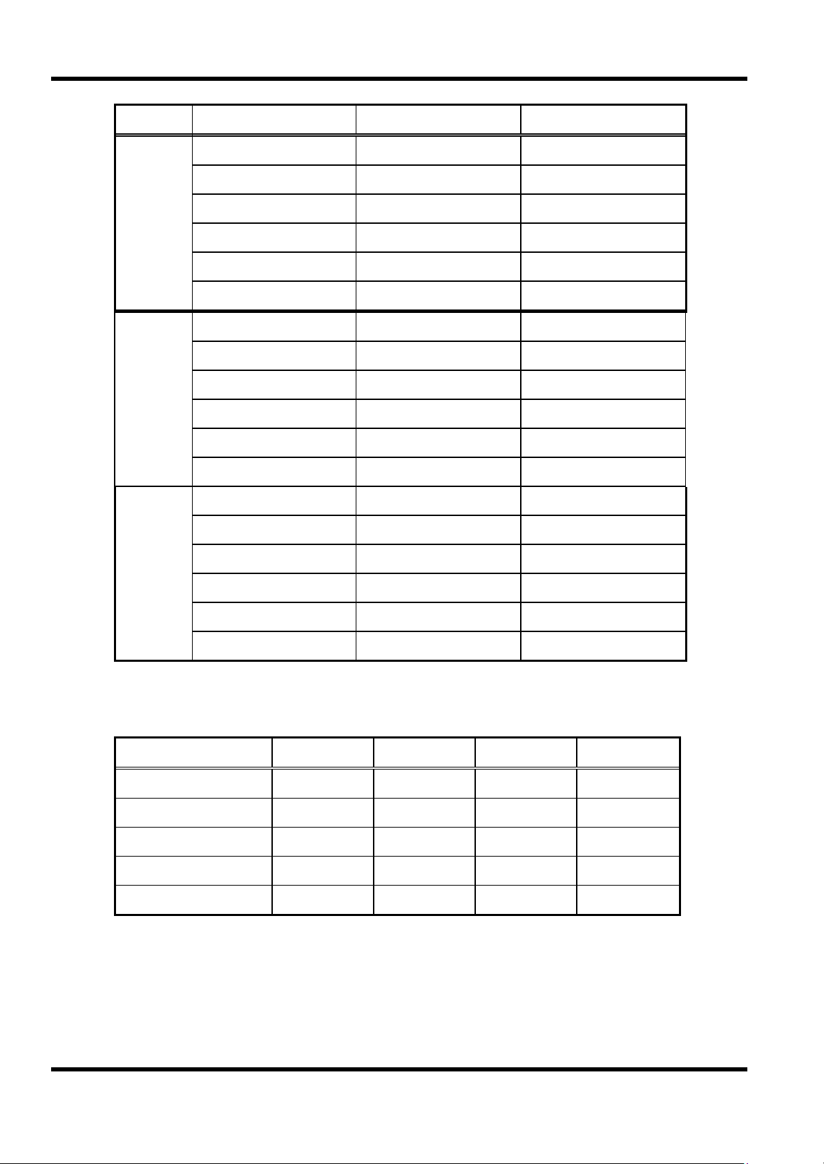
(i) OSC Type=RC ; WDT-Enable; @ Vdd=5.0 V
Cext. (F) Rext. (Ohm) Frequency (Hz) Current (A)
4.7 K 12.3M 2.1 mA
10.0 K 6.3 M 1.2 mA
3P 47.0 K 1.5 M
100.0 K 710 K
300.0 K 240 K
508 µA
385 µA
320 µA
470.0 K 155 K
This specification are subject to be changed without notice. Any latest information please preview
http;//www.mdtic.com.tw P. 9 VER1.1
310 µA
Page 10
MDT2005
Cext. (F) Rext. (Ohm) Frequency (Hz) Current (A)
4.7 K 6.2M 1.2 mA
10.0 K 3.1 M
20P 47.0 K 740 K
100.0 K 340 K
300.0 K 115 K
470.0 K 74 K
4.7 K 1.9 M
10.0 K 960 K
100P 47.0 K 215 K
100.0 K 100 K
300.0 K 35 K
470.0 K 22 K
4.7 K 765 K
10.0 K 380 K
300P 47.0 K 85 K
740 µA
385 µA
320 µA
300 µA
290 µA
560 µA
420 µA
310 µA
300 µA
285 µA
280 µA
400 µA
330 µA
285 µA
100.0 K 40 K
300.0 K 13.5 K
470.0 K 8.5 K
(ii) OSC Type=LF (C=20 p); WDT-Disable
Voltage/Frequency 32 K 455 K 1 M Sleep
2.3 V
3.0 V
4.0 V
5.0 V
6.3 V
45 µA 70 µA
78 µA 115 µA 176 µA
135 µA 120 µA 265 µA 2 µA
210 µA 275 µA 375 µA 6 µA
350 µA 420 µA 570 µA 10 µA
X
280 µA
275 µA
270 µA
<1.0 µA
<1.0 µA
This specification are subject to be changed without notice. Any latest information please preview
http;//www.mdtic.com.tw P. 10 VER1.1
Page 11
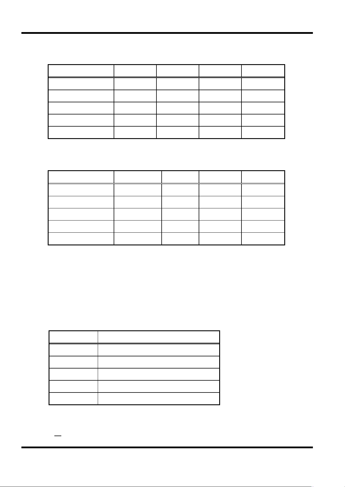
(iii) OSC Type=XT (C=10 p); WDT-Enable
Voltage/Frequency 1 M 4 M 10 M Sleep
MDT2005
2.1 V
3.0 V
4.0 V
5.0 V
6.3 V
126 µA 255 µA 535 µA
240 µA 430 µA 845 µA 2 µA
420 µA 670 µA
705 µA 945 µA
935 µA
(iv) OSC Type=HF (C=10 p); WDT-Enable
Voltage/Frequency 4 M 10 M 20 M Sleep
2.1 V
3.0 V
4.0 V
270µA 555µA 998µA
470 µA 895µA
740 µA
5.0 V 1.1 mA 1.96 mA 3.3 mA
6.3 V 1.7 mA 2.82 mA 4.7 mA
1.3 mA
1.78 mA
1.45 mA 2.55 mA
1.64 mA
1.42 mA 2.45 mA
<1.0 µA
8 µA
16 µA
32 µA
<1.0 µA
2 µA
8 µA
16 µA
32 µA
(G) Power Edge-detector Reset Voltage (Not in Sleep Mode), @ Vdd=5.0 V
Vpr≦1.1~1.3 V V
﹕Vdd (Power Supply)
pr
(H) The basic WDT time-out cycle time
@ Vdd=5.0v ,Temperature=25 ℃, the typical value as followings :
Voltage (V) Basic WDT time-out cycle time (ms)
2.3 26.4
3.0 22.7
4.0 20.1
5.0 18.1
6.3 16.4
(I) MCLRB Filter:@ Vdd=5.0v
Wm >1.2us Wm : Filter pulse width (low) in /MCLR pin.
This specification are subject to be changed without notice. Any latest information please preview
http;//www.mdtic.com.tw P. 11 VER1.1
Page 12
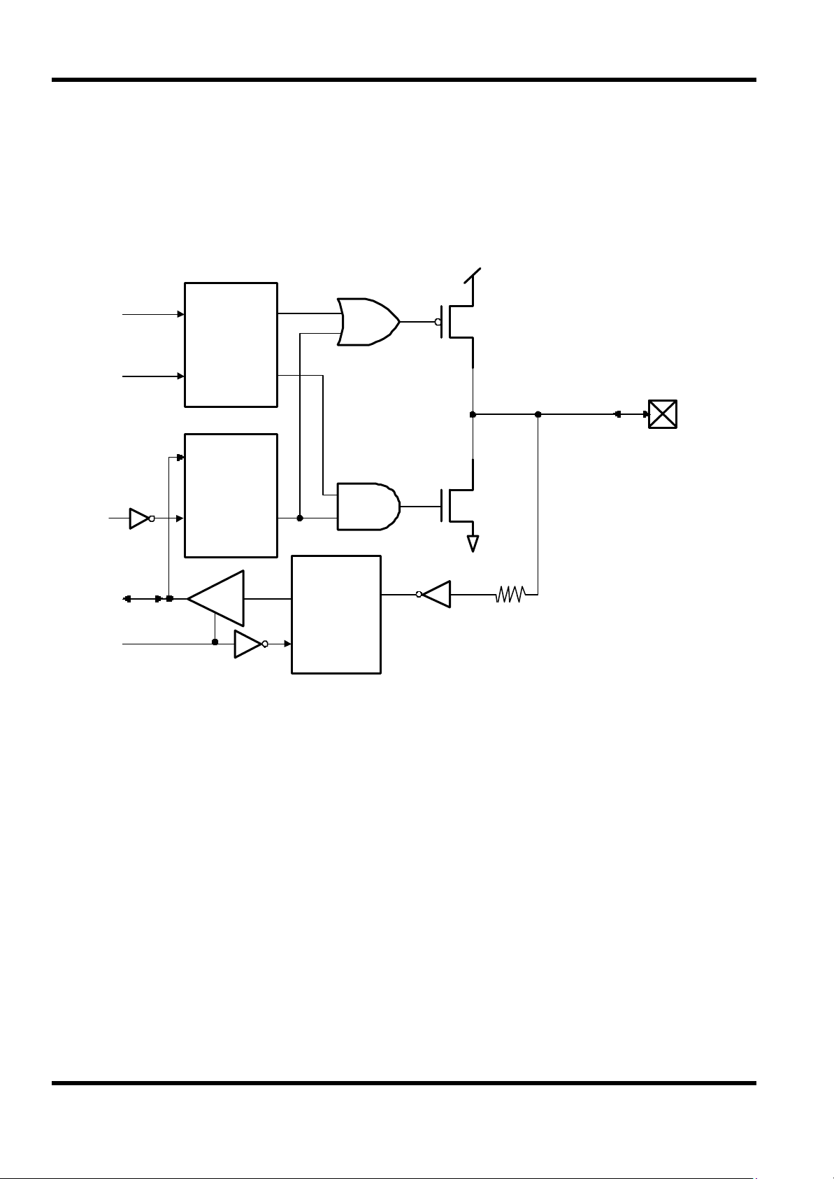
10. Port A and Port B Equivalent Circuit
MDT2005
Working Register
Data I/P
I/O Control
Write
Data Bus
Read
D
CK
D
Data O/P
CK
I/O
Control
Latch
Latch
QB
Q
Port I/O Pin
Q
QB
Data I/P
Latch
CK
D
Input Resistor
TTL Input Level
This specification are subject to be changed without notice. Any latest information please preview
http;//www.mdtic.com.tw P. 12 VER1.1
Page 13
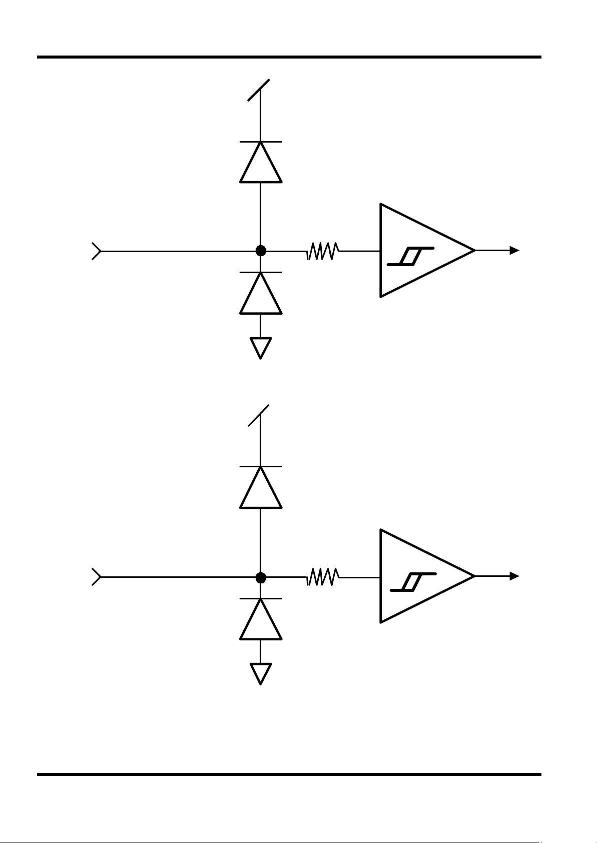
11. MCLRB and RTCC Input Equivalent Circuit
R ≒ 1 K
MCLRB
MDT2005
Schmitt Trigger
R ≒ 1 K
RTCC
Schmitt Trigger
This specification are subject to be changed without notice. Any latest information please preview
http;//www.mdtic.com.tw P. 13 VER1.1
Page 14
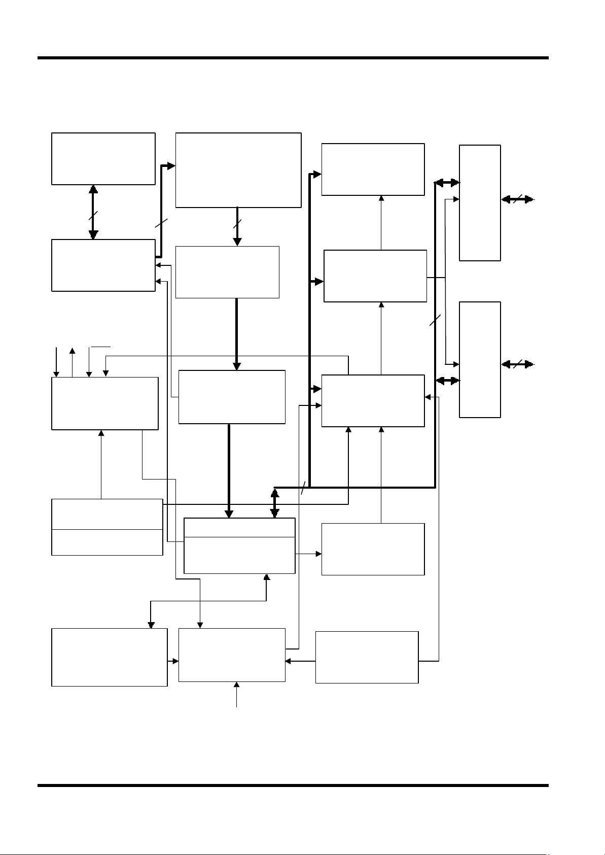
12. Block Diagram
MDT2005
Stack Two Levels
Program Counters
OSC1 OSC2
MCLR
Oscillator Circuit
9 or10 bits
512×14 (MDT2005)
9 or 10 bits
EPROM
Instruction
Register
Instruction
Decoder
14 bits
RAM
25×8
Special Register
Control Circuit
D0~D7
Port
PA0~PA3
4 bits
Port A
Port
PB0~PB7
8 bits
Port B
Power on Reset
Power Down Reset
8-bit Timer/Counter
Working Register
ALU
Prescale
RTCC
Data 8-bit
Status Register
WDT/OST
Timer
This specification are subject to be changed without notice. Any latest information please preview
http;//www.mdtic.com.tw P. 14 VER1.1
Page 15
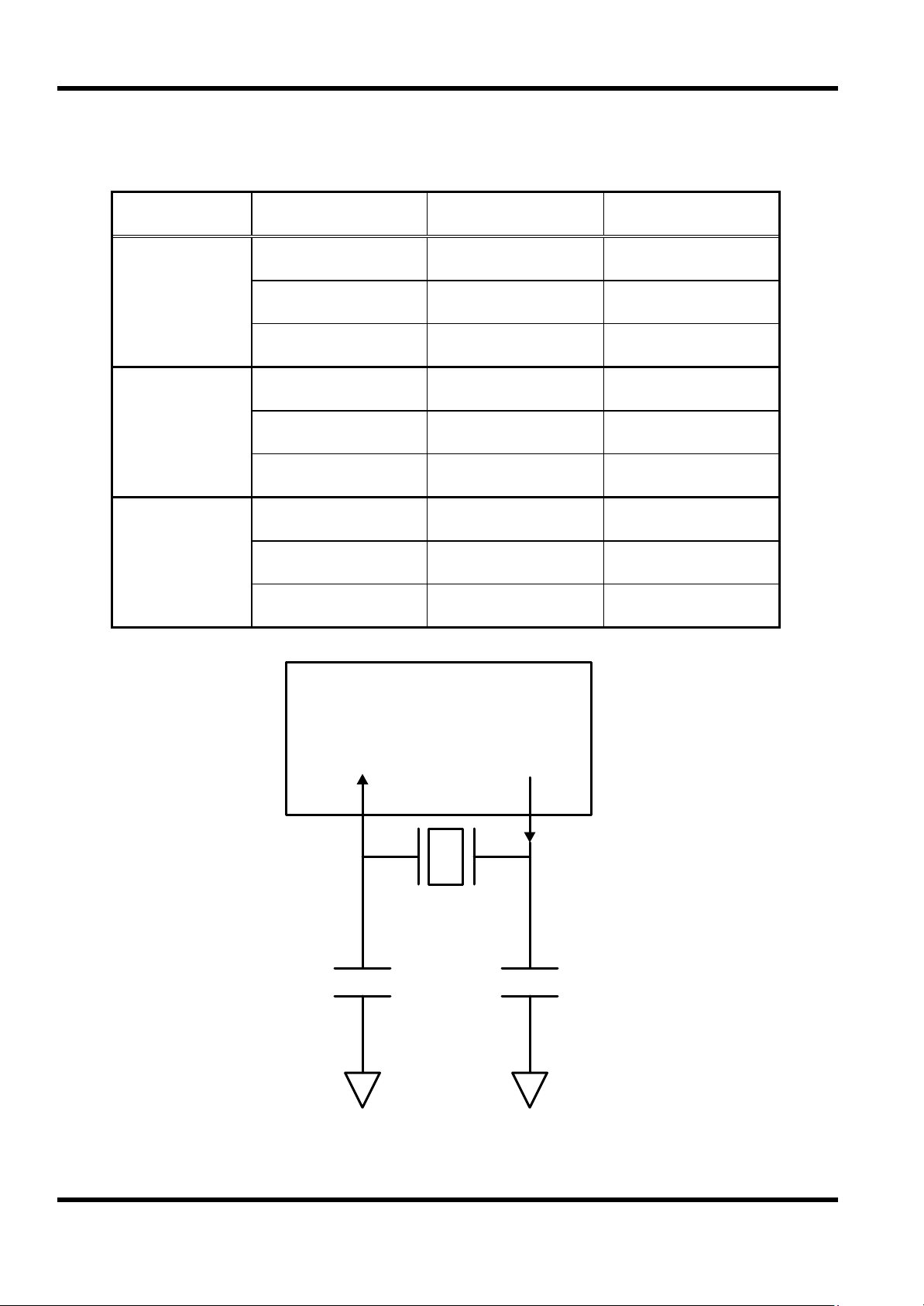
13. External Capacitor Selection For Crystal Oscillator
@ Vdd=3.0V~5.0 V
Osc. Type Resonator Freq. C1 C2
20 MHz 5 pF ~10 pF 10 pF~20 pF
HF 10 MHz 10 pF ~50 pF 20 pF ~100 pF
4 MHz 10 pF ~30 pF 20 pF ~100 pF
10 MHz 10 pF ~30 pF 10 pF ~50 pF
XT 4 MHz 10 pF ~50 pF 10 pF ~100 pF
1 MHz 10 pF ~30 pF 10 pF ~50 pF
MDT2005
1 MHz 5 pF ~10 pF 5 pF ~10 pF
LF 455 K 10 pF ~50 pF 10 pF ~50 pF
32 K 10 pF ~30 pF 20 pF ~50 pF
MDT2005
OSC1 OSC2
C1 C2
To increase the stability of oscillator and the ability of anti-noise, the above values of the external capacitor range
can be recommended for reference, but the higher capacitance also increases the start -up time.
This specification are subject to be changed without notice. Any latest information please preview
http;//www.mdtic.com.tw P. 15 VER1.1
 Loading...