

Datasheet MDS80-800, MDS50-1200, MDS50-800, MDS35-1200, MDS35-800 Datasheet (SGS Thomson Microelectronics)
...Page 1
MAIN FEATURES:
Symbol Value Unit
I
T(RMS)
V
DRM/VRRM
I
GT
50-70-85 A
800 and 1200 V
50 and 100 mA
DESCRIPTION
Packaged in ISOTOPmodules, the MDS Series is
based on the half-bridge SCR-diode configuration.
They are suitable for high power applications,
using phase controlled bridges, such as soft-start
circuits, welding equipment, motor speed
controller. The compactness of the ISOTOP
package allows high power density and optimized
power bus connections. Than ks t o their internal
ceramic pad, they provide high voltage i nsulation
(2500V RMS), complying with UL standards (File
ref: E81734).
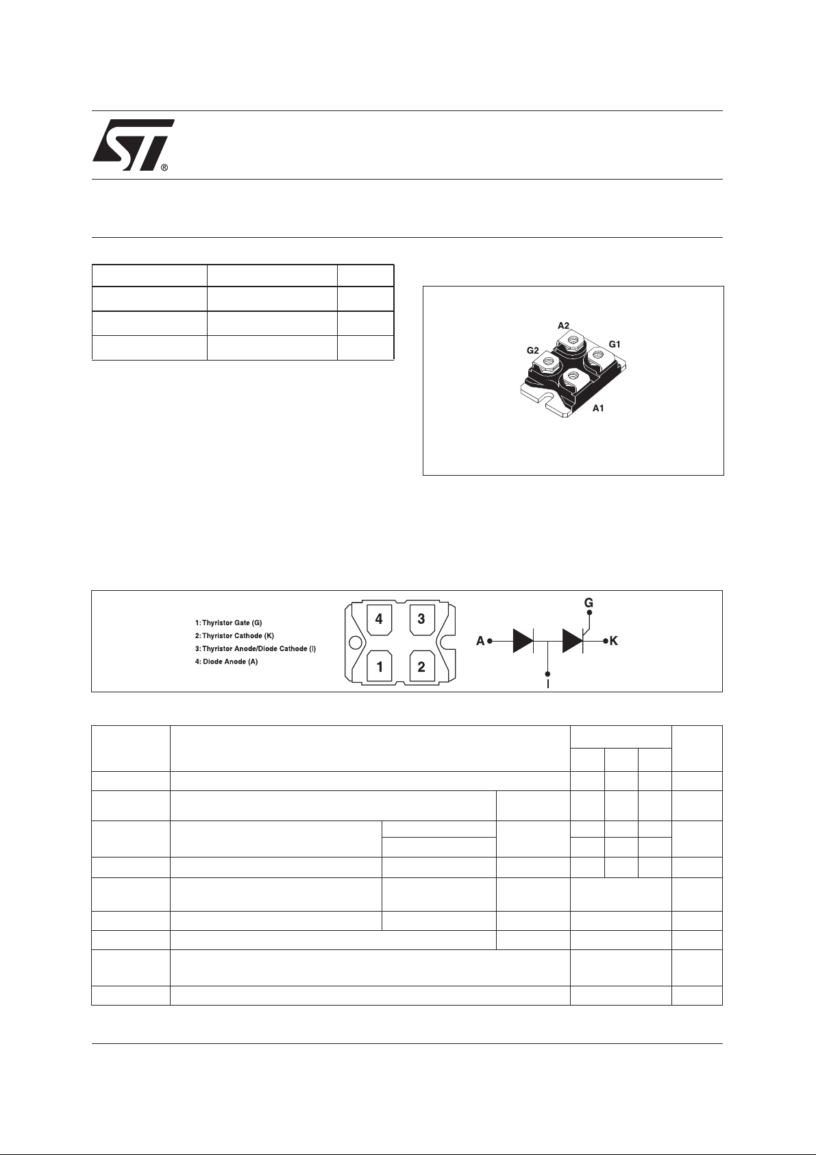
MDS35/50/80Series
DIODE / SCR MODULE
ISOTOP®
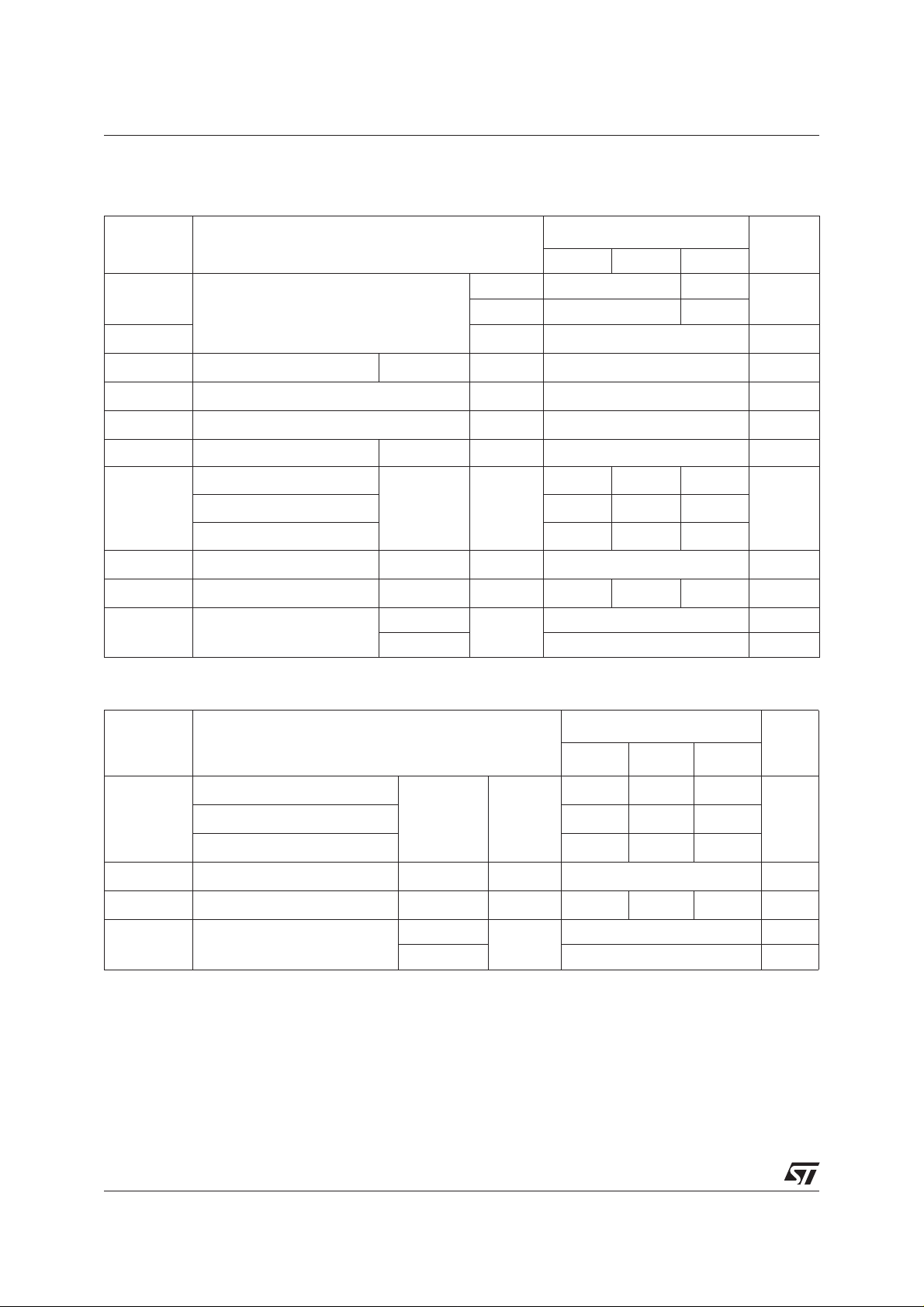
PIN CONNECTIONS
ABSOLUTE RATINGS (limiting values)
Symbol Parameter
I
T(RMS)
I
T(AV)
I
TSM
I
FSM
²
I
dI/dt
I
GM
P
G(AV)
T
stg
T
V
RGM
ISOTOP is a registred trademark of STMicroelectronics
December 2000 - Ed: 4
RMS on-state current 50 70 85 A
Averageon-state current
(Single phase-circuit, 180° conduction angle per device)
Non repetitive surge peak on-state
current (Tj initial = 25°C)
tI
j
²
t Value for fusing
Critical rate of rise of on-state current
I
=2xIGT,tr≤100 ns
G
Peak gate current tp = 20 µs Tj = 125°C 4 A
Averagegate power dissipation Tj = 125°C 1 W
Storage junction temperature range
Operating junction temperature range
Maximum peak reverse SCR gate voltage 5 V
Value
35 50 80
Tc=85°C253555 A
tp = 8.3 ms
tp = 10 ms 400 600 700
tp = 10 ms Tj = 25°C 800 1800 2450
F = 60 Hz Tj = 125°C 50 A/µs
Tj = 25°C
420 630 730
-40to+150
-40to+125
Unit
A
A
°C
2
S
1/7
Page 2
MDS35 / 5 0 / 80 Series
ELECTRICAL CHARACTERISTICS (T j = 25 °C, unless otherwise specified)
SCR
Symbol Test Conditions
I
GT
VD=12V RL=30Ω
V
GT
V
GD
I
H
I
L
dV/dt
VD=V
DRM
RL=3.3kΩ
IT= 500 mA Gate open
IG=1.2I
V
=67%V
D
GT
DRM
Gate open
Tj = 125°C MIN. 0.2 V
Tj = 125°C MIN. 1000 V/µs
ITM= 80 A tp = 380 µs
V
TM
V
t0
R
d
I
DRM
I
RRM
=110A tp=380µs
I
TM
I
=170A tp=380µs
TM
Tj = 25°C MAX.
Threshold voltage Tj = 125°C MAX. 0.85 V
Dynamic resistance Tj= 125°C MAX. 11 7.0 5.5 mΩ
V
DRM/VRRM
RATED
Tj = 25°C MAX. 20 µA
Tj = 125°C 10 mA
MDS
Unit
35 50 80
MIN. 5 10 mA
MAX. 50 100
MAX. 1.3 V
MAX. 80 mA
MAX. 120 mA
1.7 - -
-1.75-
V
--1.75
DIODE
Symbol Test Conditions
V
V
t0
R
I
R
IF=80A
F
= 110 A
I
F
= 170 A
I
F
Threshold voltage Tj = 125°C MAX. 0.85 V
Dynamic resistance Tj = 125°C MAX. 11 7.0 5.5 mΩ
d
VR=V
RRM
MDS
Unit
35 50 80
V
Tj = 25°C MAX.
1.7 - -
-1.7-
--1.7
Tj = 25°C MAX. 20 µA
Tj = 125°C 10 mA
2/7
Page 3
MDS35 / 50 / 80 Series
THERMAL RESISTANCES
Symbol Parameter Value Unit
R
th(j-c)
Junction to case (DC) MDS35 1.00 °C/W
MDS50 0.75
MDS80 0.45
PRODUCT SELECTOR
PartNumber
MDS35-xxx X X 50 mA
MDS50-xxx X X 50 mA
MDS80-xxx X X 150 mA
Voltage (xxx)
Sensitivity
800 V 1200 V
ORDERING INFORMATION
SCR
MODULE
SERIES
VOLTAGE:
800: 800V
1200: 1200V
CURRENT:
35: 50A
50: 70A
80: 85A
Package
ISOTOP
TM
OTHER INFORMATION
Part Number Marking Weight Base Quantity Packing mode
MDS35-xxx MDS35-xxx 27.0 g 10 Tube
MSDS50-xxx MDS50-xxx 27.0 g 10 Tube
MDS80-xxx MDS80-xxx 27.0 g 10 Tube
Note:xxx=voltage
3/7
Page 4

MDS35 / 5 0 / 80 Series
Fig. 1-1: Maximum average power dissipation
versus average on-state current (thyristor or
diode, sinusoïdal waveform).
Fig. 1-3: Maximum total power dissipation versus
output current on resistive or indu ctive load
(Single phase bridge rectifier, two packages).
Fig. 1-2: M aximum average power dissipation
versus average on-state current (thyristor or
diode, rectangular waveform).
Fig. 1-4: Maximum total power dissipation versus
output current (Three phase bridge rectifier,three
packages).
Fig. 2-1: Average on-state current versus case
temperature (thyristor or diode, sinusoïdal
waveform).
4/7
Fig. 2-2: Average on-state c urrent versus case
temperature (thyristor or diode, rectangular
waveform).
Page 5

MDS35 / 50 / 80 Series
Fig. 3: Relative variation of thermal impedance
junction to case versus pulse duration.
Fig. 5-1: Surge peak on-state current versus
number of cycles (MDS35 and MDS 50).
Fig. 4: Relative variation of gate trigger current,
holding current and latching current versus
junction temperature (t ypical values).
Fig. 5-2: Surge peak o n-state current versus
number of cycles (MDS80).
Fig. 6-1: Non-repetitive surge peak on-state
current for a sinusoidal pulse with width
tp < 10 ms, and corresponding value of I²t
(MDS35 and MDS50).
Fig. 6-2: Non repe titive surge peak on-st ate
current for a sinusoidal pulse with w i dth
tp < 10 ms, and corresponding value of I²t
(MDS80).
5/7
Page 6

MDS35 / 5 0 / 80 Series
Fig. 7-1: On-state characteristics (thyristor or
diode, maximum values) (MDS35).
Fig. 7-3: On-state characteristics (thyristor or
diode, maximum values) (MDS80).
Fig. 7-2: On-state characteristics (thyristor o r
diode, maximum values) (MDS50).
6/7
Page 7

PACKAGE MECHANICAL DATA
ISOTOP™
MDS35 / 50 / 80 Series
DIMENSIONS
REF.
Millimeters Inches
Min. Max. Min. Max.
A 11.80 12.20 0.465 0.480
A1 8.90 9.10 0.350 0.358
B 7.8 8.20 0.307 0.323
C 0.75 0.85 0.030 0.033
C2 1.95 2.05 0.077 0.081
D 37.80 38.20 1.488 1.504
D1 31.50 31.70 1.240 1.248
E 25.15 25.50 0.990 1.004
E1 23.85 24.15 0.939 0.951
E2 24.80 typ. 0.976 typ.
G 14.90 15.10 0.587 0.594
G1 12.60 12.80 0.496 0.504
G2 3.50 4.30 0.138 0.169
F 4.10 4.30 0.161 0.169
F1 4.60 5.00 0.181 0.197
P 4.00 4.30 0.157 0.69
P1 4.00 4.40 0.157 0.173
S 30.10 30.30 1.185 1.193
■ Recommended torque value: 1.3 Nm (max. 1. 5 Nm) for the 6 x M4 screws (2 x M 4 screws recom-
mended for mounting t he package on the hea tsink and the 4 provided screws.
■ The screws supplied with the package are adapted for mounting on a board (or other types of termi-
nals) with a thickness of 0.6 mm min. and 2.2 mm max.
Information furnished is believed to be accurate and reliable. However, STMicroelectronics assumes no responsibility for the consequences
ofuse ofsuchinformationnorfor anyinfringementofpatentsor other rightsof third partieswhichmay result from its use. No licenseisgranted
by implication or otherwise under any patentorpatent rights of STMicroelectronics. Specifications mentioned in this publication are subject
to change without notice. This publication supersedes and replaces all information previously supplied. STMicroelectronics products are not
authorized for use as critical components in life support devices or systems without express written approval of STMicroelectronics.
© TheST logois a registeredtrademark of STMicroelectronics
© 2000 STMicroelectronics - Printed in Italy - All Rights Reserved
Australia - Brazil - China - Finland - France - Germany - Hong Kong - India - Italy - Japan - Malaysia - Malta - Morocco
STMicroelectronics GROUP OF COMPANIES
Singapore- Spain - Sweden -Switzerland - United Kingdom
http://www.st.com
7/7
 Loading...