

Page 1
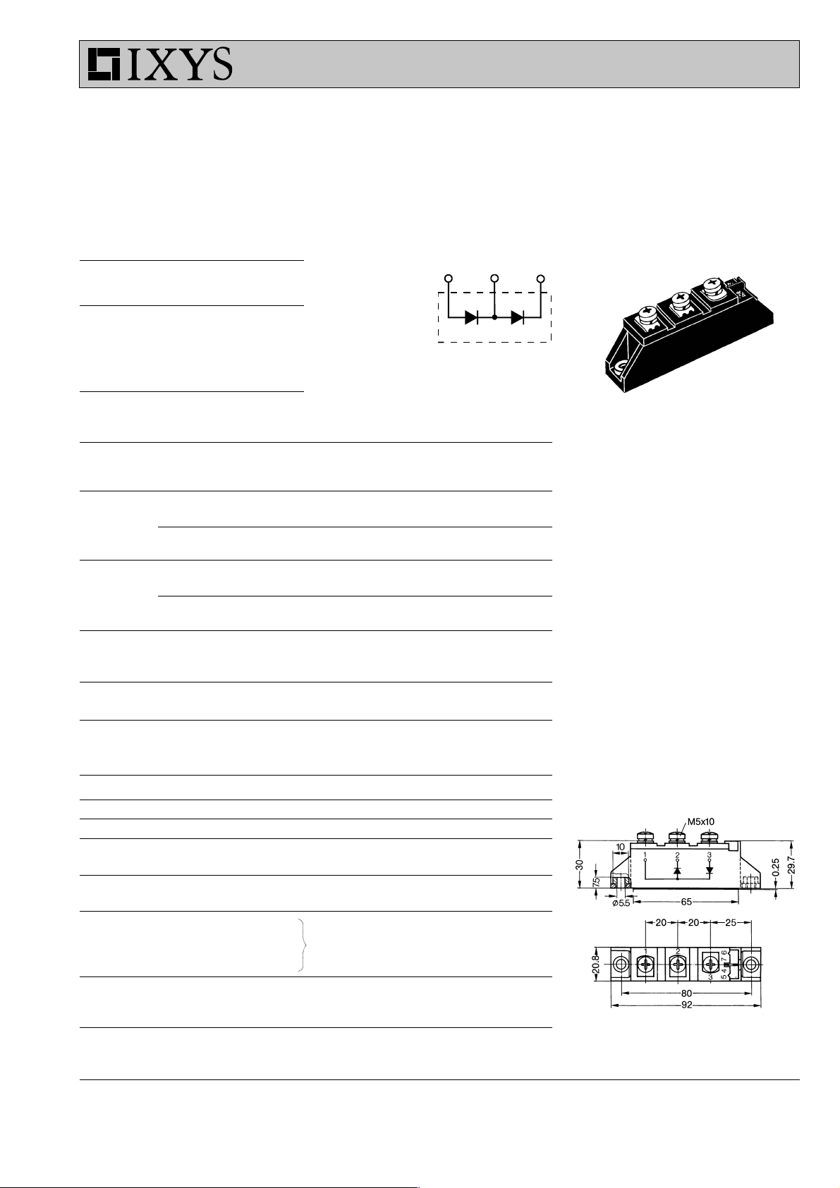
MDD 56
Diode Modules
V
RSM
VV
900 800 MDD 56-08N1 B
1300 1200 MDD 56-12N1 B
1500 1400 MDD 56-14N1 B
1700 1600 MDD 56-16N1 B
1900 1800 MDD 56-18N1 B
Symbol Test Conditions Maximum Ratings
I
FRMS
I
FAVM
I
FSM
òi2dt TVJ = 45°C t = 10 ms (50 Hz), sine 9800 A2s
T
VJ
T
VJM
T
stg
V
ISOL
M
d
Weight Typical including screws 90 g
V
RRM
TVJ = T
TC = 75°C; 180° sine 95 A
Type
VJM
150 A
TC = 100°C; 180° sine 71 A
TVJ = 45°C; t = 10 ms (50 Hz), sine 1400 A
VR = 0 t = 8.3 ms (60 Hz), sine 1650 A
= T
T
VJ
VJM
VR = 0 t = 8.3 ms (60 Hz), sine 1400 A
t = 10 ms (50 Hz), sine 1200 A
VR = 0 t = 8.3 ms (60 Hz), sine 11300 A2s
= T
T
VJ
VJM
VR = 0 t = 8.3 ms (60 Hz), sine 8100 A2s
t = 10 ms (50 Hz), sine 7200 A2s
-40...+150 °C
150 °C
-40...+125 °C
50/60 Hz, RMS t = 1 min 3000 V~
£ 1 mA t = 1 s 3600 V~
I
ISOL
Mounting torque (M5) 2.5-4/22-35 Nm/lb.in.
Terminal connection torque (M5) 2.5-4/22-35 Nm/lb.in.
I
FRMS
I
FAVM
V
TO-240 AA
= 2x 150 A
= 2x 95 A
= 800-1800 V
RRM
1
3312
2
Features
●
International standard package
JEDEC TO-240 AA
●
Direct copper bonded Al2O3 -ceramic
base plate
●
Planar passivated chips
●
Isolation voltage 3600 V~
●
UL registered, E 72873
Applications
●
Supplies for DC power equipment
●
DC supply for PWM inverter
●
Field supply for DC motors
●
Battery DC power supplies
Advantages
●
Space and weight savings
●
Simple mounting
●
Improved temperature and power
cycling
●
Reduced protection circuits
Symbol Test Conditions Characteristic Values
I
R
V
F
V
T0
r
T
Q
S
I
RM
R
thJC
R
thJK
d
S
d
A
a Maximum allowable acceleration 50 m/s
Data according to IEC 60747 and refer to a single diode unless otherwise stated.
IXYS reserves the right to change limits, test conditions and dimensions
TVJ= T
IF = 200 A; TVJ = 25°C 1.48 V
For power-loss calculations only 0.8 V
TVJ = T
TVJ = 125°C; IF = 50 A, -di/dt = 3 A/ms 100 mC
per diode; DC current 0.51 K/W
per module other values 0.255 K/W
per diode; DC current see Fig. 6/7 0.71 K/W
per module 0.355 K/W
Creepage distance on surface 12.7 mm
Strike distance through air 9.6 mm
VJM
VJM
; VR = V
RRM
10 mA
3mW
24 A
© 2000 IXYS All rights reserved
Dimensions in mm (1 mm = 0.0394")
2
1 - 3
Page 2
MDD 56
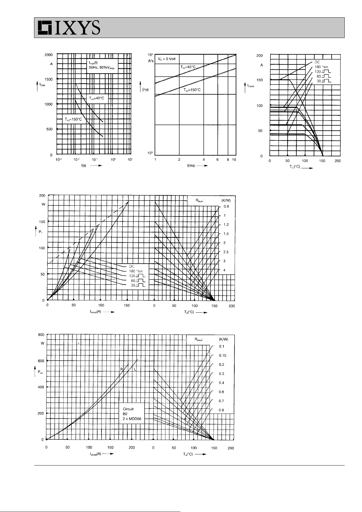
Fig. 1 Surge overload current
I
: Crest value, t: duration
FSM
Fig. 2 òi2dt versus time (1-10 ms) Fig. 2a Maximum forward current
at case temperature
Fig. 3 Power dissipation versus
forward current and ambient
temperature (per diode)
Fig. 4 Single phase rectifier bridge:
Power dissipation versus direct
output current and ambient
temperature
R = resistive load
L = inductive load
© 2000 IXYS All rights reserved
2 - 3
Page 3

MDD 56
Fig. 5 Three phase rectifier bridge:
Power dissipation versus direct
output current and ambient
temperature
Fig. 6 Transient thermal impedance
junction to case (per diode)
R
for various conduction angles d:
thJC
d R
thJC
(K/W)
DC 0.51
180° 0.53
120° 0.55
60° 0.58
30° 0.62
Constants for Z
iR
calculation:
thJC
(K/W) ti (s)
thi
1 0.013 0.0015
2 0.055 0.045
3 0.442 0.485
Fig. 7 Transient thermal impedance
junction to
for various conduction angles d:
R
thJK
d R
heatsink (per diode)
(K/W)
thJK
DC 0.71
180° 0.73
120° 0.75
60° 0.78
30° 0.82
© 2000 IXYS All rights reserved
Constants for Z
iR
calculation:
thJK
(K/W) ti (s)
thi
1 0.013 0.0015
2 0.055 0.045
3 0.442 0.485
4 0.2 1.25
3 - 3
 Loading...