

Page 1
Cellular CDMA Upconverter / Driver
820 - 850 MHz
MD59-0039
Features
• Highly integrated upconverter and driver amplifier
• High linear output power, +5 dBm
• Variable gain control
• Low LO drive level, -5 dBm
• Single 3.0 V supply
• Miniature 5 mm MLF plastic package
Description
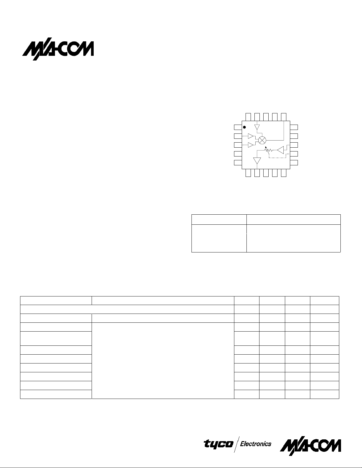
M/A-COM’s MD59-0039 upconverter IC for cellular CDMA
applications integrates a mixer, RF amplifier, IF amplifier, and
LO buffer in a 5 millimeter (mm) square plastic micro leadframe package with exposd back side for improved high
frequency grounding.
M/A-COM designed the MD59-0039 to operate with balanced
IF inputs and a single-ended RF output with a frequency in the
800 to 900 MHz frequency band. The maximum conversion
gain is 24 dB, with a minimum 15 dB of gain range. The
MD59-0039 can produce 5 dBm of linear output power, with an
associated ACPR of - 56 dBc (IS-98). An internal LO buffer
amplifier allows the device to accommodate low LO drive levels
in the range of - 10 dBm to - 5 dBm.
M/A-COM fabricates the MD59-0039 using a 0.5 micron low
noise GaAs MESFET process. The process features full
passivation for increased performance and reliability.
Functional Block Diagram
LO IN
LO SRC
20
IF IN+
IF IN-
IF+ VDD
IF- VDD
1
DRV OUT
DRV SRC 2
LOA VDD
MIX OUT
GND
GND
RFA VDD
RFA SRC
RFA IN
VVA CNTL
DRV SRC1
GND
DRV VDD2
DRV VDD1
Ordering Information
Part Number Package
MD59-0039 MLF-5.0 mm Plastic Package
MD59-0039TR Forward Tape and Reel1
MD59-0039RTR Reverse Tape and Reel1
1. If specific reel size is required, consult factory for part number
assignment.
Electrical Specifications TA = +25° C, VDD = 3.0 Volts
Parameter Test Conditions Units Min. Typ. Max.
Cascaded Performance
RF Frequency MHz 820 850
Conversion Gain Frequency = 836 MHz, PIN = -15 dBm dB 24
Linear Ouput Power @
ACPR of –56 dBc (IS-98)
Gain Range
Port Matches (all ports)
LO-to-RF Isolation
LO-to-IF Isolation
RF-to-IF Isolation
I
DD
Specifications subject to change without notice.
North America: Tel. (800) 366-2266, Fax (800) 618-8883
Asia/Pacific: Tel.+81-44-844-8296, Fax +81-44-844-8298
Europe: Tel. +44 (1344) 869 595, Fax+ 44 (1 34 4) 30 0 020
Visit www.macom . com for ad di tional data sheets and pr o d uct i nf orm ation.
dBm +5.0
dB 15
dB 10
dB 40
dB 30
dB 20
mA 80
V 2.0
1
Page 2
Cellular CDMA Upconverter / Driver, 820 - 850 MHz
MD59-0039
Electrical Specifications TA = +25° C, VDD = 3.0 Volts (Cont’d)
Parameter Test Conditions Units Min. Typ. Max.
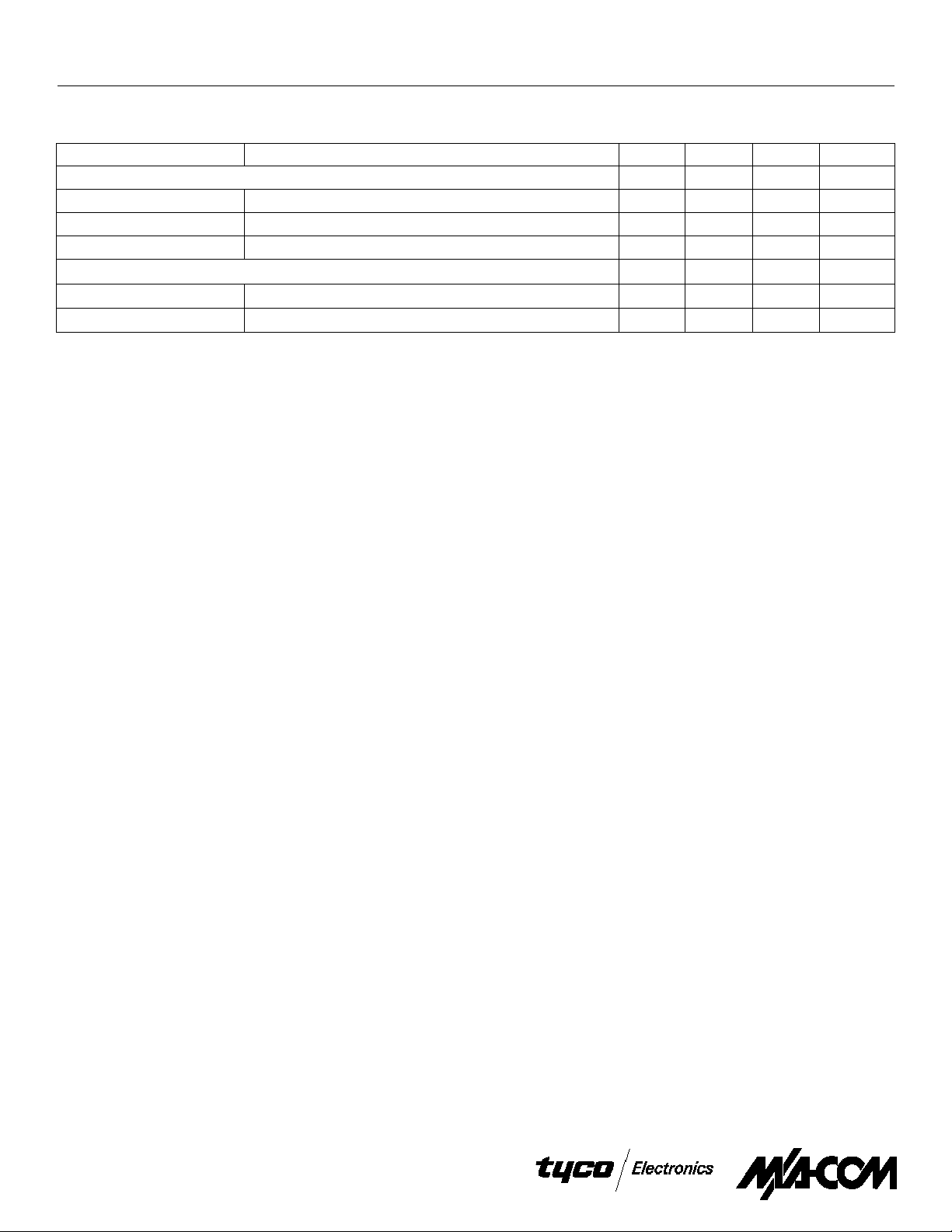
IF Input
IF Frequency MHz 130
IF Input Level dBm -16
IF Impedance Balanced ohms 265
LO Input
LO Frequency MHz 954 979
LO Input Level dBm -10 -5 0
Operating Instructions
The MD59-0039 is a highly integrated MMIC upconverter for
the 800 – 900 MHz cellular band. The upconverter provides
exceptional RF performance while drawing low DC current and
is packaged in a low cost plastic package. It is an ideal
candidate for light-weight, battery operated, portable handset
applications.
The MD59-0039 incorporates a differential IF amplifier,
balanced mixer, LOA, RFA, variable voltage attenuator and a
two-stage driver amplifier. Surface mount resistors, inductors
and capacitors are used in conjunction with the MMIC to
optimize the trade-offs between performance, tunability and
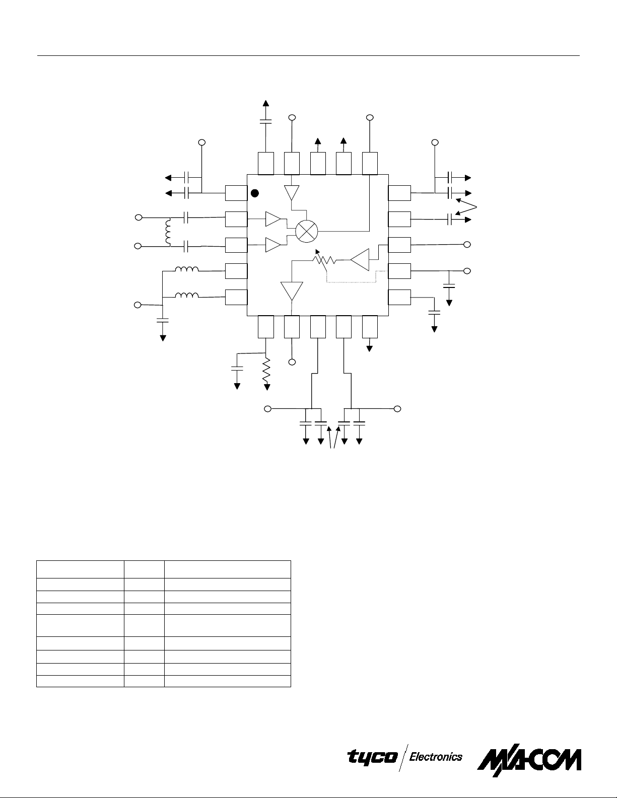
ease of use. The schematic on the previous page shows the
MMIC and required off-chip component values.
The input impedance of the differential IF amplifier is matched
externally to 50 Ω at the desired IF frequency with L1, C1 and
C2. In addition, C1 and C2 also act as DC blocking capacitors
for the differential IF inputs. A 06-03 case style can be used for
L1 in most cases, but a 08-05 case style can be used if more gain
is required. Capacitor C3 is a low frequency bypass capacitor.
Inductors L2 and L3 help match the output of the differential IF
amplifier to the differential input of the mixer, as well as
providing RF chokes for the DC supply lines.
The LO input port is matched on chip to 50 Ω. The LO buf fer
amplifier provides the voltage gain required to drive the gat e of
the mixer FET, while drawing a minimal amount of current.
The LO buffer amplifies the –10 dBm input signal to the level
required to drive the mixer. For optimum performance, it is
recommended to use a drive level of –3 dBm. C7 and C14 are
RF and low frequency bypass capacitors for the DC supply line.
Capacitor C13 is a source bypass capacitor for the LO amplifier.
The position of both C7 and C13 shown in the application
circuit may affect the gain of the RF amplifier and should be
placed as close the device as is practical.
The mixer is a balanced floating FET mixer that provides
exceptional linearity and isolation with low loss and no DC
current. The mixer uses a high side LO frequency. An external
image reject filter is required between the mixer output and RFA
input to prevent upconversion noise at the image frequency from
leaking onto the RF. This filter should have 50 Ω input and
output impedance.
The topology of both the input and output matching networks
for the RF amplifier provides internal DC blocking capacitors, to
prevent unwanted DC leakage. C6 and C12 are RF and low
frequency bypass capacitors for the DC supply line. Capacitor
C11 is a source bypass capacitor for the RF amplifier. Similar to
the LOA, C11 and C12 should be placed as close the device as is
practical. The VVA is a T-attenuator topology, providing better
than 30 dB of attenuation from 800 to 900 MHz.
The two-stage driver amplifier is nominally biased with 40 mA.
An external resistor, R1, can be used to adjust the bias current of
the second stage, thereby adjusting the linear output power. C4,
C5, C9 and C10 are RF and low frequency bypass capacitors for
the DC supply lines, for the first and second stage of the driver
respectively. Capacitors C8 and C16 are the source bypass
capacitors for the driver amplifier.
Specifications subject to change without notice.
North America: Tel. (800) 366-2266, Fax (800) 618-8883
Asia/Pacific: Tel.+81-44-844-8296, Fax +81-44-844-8298
Europe: Tel. +44 (1344) 869 595, Fax+ 44 (1 34 4) 30 0 020
Visit www.macom . com for ad di tional data sheets and pr o d uct i nf orm ation.
V 2.0
2
Page 3
Cellular CDMA Upconverter / Driver, 820 - 850 MHz
MD59-0039
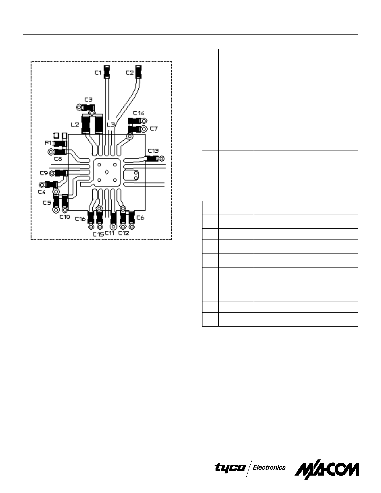
Recommended PCB Configuration
Pin Configuration
Pin # Pin Name Description
1 LOA VDD LO amplifier supply voltage. RF bypass-
ing required
2 IF+ IN RF input to differential IF amplifier. DC
blocked
3 IF- IN RF input to differential IF amplifier. DC
blocked
4 IF+ VDD Differential IF amplifier supply voltage.
RF bypassing required
5 IF- VDD Differential IF amplifier supply voltage.
RF bypassing required
6 DRV SRC2 Source of RFA output stage FET. Off-
chip resistor may be used for current
control. RF bypassing required
7 DRV OUT 50 ohm output of driver amplifier
8 DRV VDD2 2nd stage driver amplifier supply voltage.
RF bypassing required
9 DRV VDD1 1st stage driver amplifier supply voltage.
RF bypassing required
10 GND DC and RF ground
11 DRV SRC1 1st stage source of driver amplifier. RF
bypassing required
12 VVA CNTRL Control voltage input to voltage variable
attenuator
13 RFA IN 50 ohm input of RF amplifier
14 RFA SRC Source of RF amplifier. RF bypassing
required
15 RFA VDD RF amplifier supply voltage. RF bypass-
ing required
16 MIX OU T RF output of downconverter
17 GND DC and RF ground
18 GND DC and RF ground
19 LO IN Local oscillator Input (-5 dBm typical)
20 LO SRC Source of LO amplifier. RF bypassing
required
Specifications subject to change without notice.
North America: Tel. (800) 366-2266, Fax (800) 618-8883
Asia/Pacific: Tel.+81-44-844-8296, Fax +81-44-844-8298
Europe: Tel. +44 (1344) 869 595, Fax+ 44 (1 34 4) 30 0 020
Visit www.macom . com for ad di tional data sheets and pr o d uct i nf orm ation.
V 2.0
3
Page 4
Cellular CDMA Upconverter / Driver, 820 - 850 MHz
Sample Board Schematic
MD59-0039
IF+
IN
IFIN
IF
Vdd
L1
C3
C14
C7
L2
L3
LOA
Vdd
C2
C1
C8
1
C13
R1
20
LO
In
Driver
Out
Mixer
Out
RFA
Vdd
C6
C12,
C11
RFA
In
VVA
Control
C15
C16
External Circuitry Parts List
Ref. Designation Value Purpose
L1 270 nH IF match
L2, L3 68 nH IF match
C3, C4, C5, C6, C7 1000 pF RF bypass
C8, C9, C10, C11, C12,
C13, C14
C1, C2 1000 pF IF matching
C16 15 pF RF bypass
C15 47 pF RF bypass
R1 33 ohm Current control from driver 2
150 pF RF bypass
Driver
Vdd2
nd
stage
C9
Driver
Vdd1
C10
C4, C5
Specifications subject to change without notice.
North America: Tel. (800) 366-2266, Fax (800) 618-8883
Asia/Pacific: Tel.+81-44-844-8296, Fax +81-44-844-8298
Europe: Tel. +44 (1344) 869 595, Fax+ 44 (1 34 4) 30 0 020
Visit www.macom . com for ad di tional data sheets and pr o d uct i nf orm ation.
V 2.0
4
Page 5
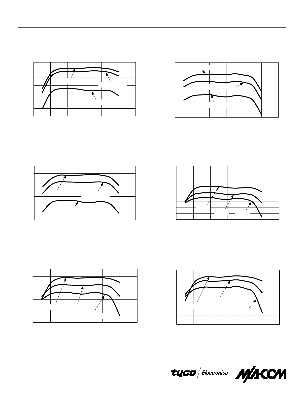
Cellular CDMA Upconve rter / Driver, 820 - 850 MH z
Typical Performance Curves
MD59-0039
Conversion Gain vs. VVA CNTRL, T = -30° C,
LO=-5dBm, IF=-15dBm, VBatt and VR5=3.0V
30
25
20
15
10
5
CONVERSION GAIN (dB)
0
-5
810 820 830 840 850 860 870
VVA CNTRL = 2.7 V
VVA CNTRL = 1.7 V
VVA CNTRL = 0.7 V
RF FREQUENCY (MHz)
Conversion Gain vs. VVA CNTRL, T = +25° C
LO=-5dBm, IF=-15dBm, VBatt and VR5=3.0V
30
25
20
15
10
5
0
CONVERSION GAIN (dB)
-5
810 820 830 840 850 860 870
VVA CNTRL = 2.7 V
VVA CNTRL = 0.7 V
RF FREQUENCY (MHz)
VVA CNTRL = 1.7 V
Conversion Gain vs. VVA CNTRL, T = +85° C,
LO=-5dBm, IF=-15dBm, VBatt and VR5=3.0V
30
25
20
15
10
5
0
-5
CONVERSION GAIN (dB)
-10
-15
810 820 830 840 850 860 870
VVA CNTRL = 2.7 V
VVA CNTRL = 1.7 V
VVA CNTRL = 0.7 V
RF FREQUENCY (MHz)
Conversion Gain vs. Temperature,
VVA CNTRL=0.7V, LO=-5dBm, IF=-15dBm,
VBatt and VR5 = 3.0V
30
25
20
15
10
5
0
-5
CONVERSION GAIN (dB)
-10
-15
810 820 830 840 850 860 870
T = -30 C
T = +25 C
RF FREQUENCY (MHz)
T = + 85 C
Conversion Gain vs. Temperature
VVA CNTRL=1.7V, LO=-5dBm, IF=-15dBm,
VBatt and VR5 = 3.0V
30
25
20
15
10
5
0
CONVERSION GAIN (dB)
-5
810 820 830 840 850 860 870
Specifications subject to change without notice.
North America: Tel. (800) 366-2266, Fax (800) 618-8883
Asia/Pacific: Tel.+81-44-844-8296, Fax +81-44-844-8298
Europe: Tel. +44 (1344) 869 595, Fax+ 44 (1 34 4) 30 0 020
Visit www.macom . com for ad di tional data sheets and pr o d uct i nf orm ation.
T = -30 C
T = +25 C
T = + 85 C
RF FREQUENCY (MHz)
Conversion Gain vs. Temperature
VVA CNTRL=2.7V, LO=-5dBm, IF=-15dBm,
VBatt and VR5 = 3.0V
30
25
20
15
10
5
CONVERSION GAIN (dB)
0
810 820 830 840 850 860 870
T = -30 C
T = +25 C
T = + 85 C
RF FREQUENCY (MHz)
V 2.0
5
Page 6
)
)
Cellular CDMA Upconverter / Driver, 820 - 850 MHz
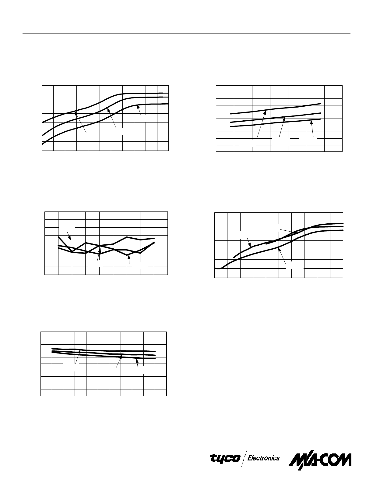
Typical Performance Curves (Cont’d)
MD59-0039
Conversion Gain vs. VVA CNTRL Over
Temperature, RF Frequency = 835 MHz,
LO=-5dBm, IF=-15dBm, VBatt and VR5=3.0V
30
25
20
15
10
5
CONVERSION GAIN (dB)
0
-5
0.5 0.7 0.9 1.1 1.3 1.5 1.7 1.9 2.1 2.3 2.5 2.7
T = -30 C
VVA CNTRL (Volts)
T = +25 C
T = + 85 C
ACPR vs. Frequency Over Temperature
Linear Output @ ACPR = -56dBc, LO=-5 dBm
IF=-15dBm (-14dBm @ COLD),
VBatt and VR5=3.0V
7.0
6.5
6.0
5.5
5.0
4.5
4.0
3.5
Output Power @ -56 dBc (dBm)
3.0
T = +85 C
T = -30 C
815 820 825 830 835 840 845 850 855 860
RF FREQUENCY (MHz)
T = +25 C
LO_IN to MIX_OUT Isolation Over
Temperature, LO = -5dBm,
VBatt and VR5 = 3.0V
25
24
23
22
21
20
19
18
17
LO_IN to MIX_OUT Isolation (dB
16
15
820 825 830 835 840 845 850 855
T = -30 C
T = +25 C
T = +85 C
RF FREQUENCY (MHz)
Linear Output Power vs. VVA_CNTRL, Over
Temperature, LO=-5dBm, IF=-15dBm
(-14 dBm @ COLD), VBatt and VR5 = 3.0V
15
10
5
0
-5
-10
OUTPUT POWER (dBm
-15
-20
0.70.91.11.31.51.71.92.12.32.52.7
T = -30 C
T = +25 C
T = +85 C
VVA CNTRL (Volts)
MIX_OUT to VGA_IN Isolation Over
Temperature, LO=-5dBm,
VBatt and VR5 = 3.0V
37
36
35
34
33
32
31
30
29
28
MIX_OUT to VGA_IN Isolation (dB
27
810 815 820 82 5 830 835 840 845 850 855 860 865
Specifications subject to change without notice.
North America: Tel. (800) 366-2266, Fax (800) 618-8883
Asia/Pacific: Tel.+81-44-844-8296, Fax +81-44-844-8298
Europe: Tel. +44 (1344) 869 595, Fax+ 44 (1 34 4) 30 0 020
Visit www.macom. com for ad ditional data sheets an d pr o d uct inf or m ati o n.
T = -30 C
T = +85 C T = +25 C
RF FREQUENCY (MHz)
V 2.0
6
Page 7
Cellular CDMA Upconverter / Driver, 820 - 850 MHz
MD59-0039
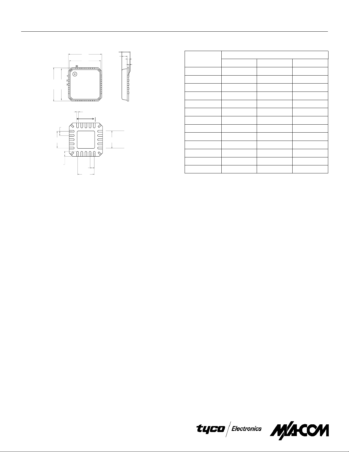
5 mm MLF - 201
D2
E2
A2
A
A3
A1
D
D1
EE1
20 x b
e
4 x e
L
1. See JEDEC MO-220A VGGD- for additional dimensional and
tolerance information
e
4 x e
5 mm MLF - 20
Dim.
A 0.80 0.90 1.00
A1 0 0.02 0.05
A2 0 0.65 1.00
A3 0.25 ref.
b 0.23 0.30 0.38
D 5.00 basic
D1 4.75 basic
D2 1.25 2.70 3.25
e 0.65 basic
E 5.00 basic
E1 4.75 basic
E2 1.25 2.70 3.25
L 0.35 0.55 0.75
Measurement (mm)
Min. Nom. Max.
Specifications subject to change without notice.
North America: Tel. (800) 366-2266, Fax (800) 618-8883
Asia/Pacific: Tel.+81-44-844-8296, Fax +81-44-844-8298
Europe: Tel. +44 (1344) 869 595, Fax+ 44 (1 34 4) 30 0 020
Visit www.macom. com for ad ditional data sheets an d pr o d uct inf or m ati o n.
V 2.0
7
 Loading...