

(1)
PCS CDMA Upconverter / Driver
PCS CDMA Upconverter / Driver
PCS CDMA Upconverter / DriverPCS CDMA Upconverter / Driver
1710
1710————1910 MHz
17101710
1910 MHz
1910 MHz1910 MHz
MD59-0022
Features
• High Integrated Upconverter and Driver IC
• Operates over 2.7 V to 5V Supply Voltage
• +9 dBm Output Power at 51 dBc ACPR
• Low current mode for power saving at low output power
• Balanced IF Input 265 Ω
• Low LO Drive Level -10 dBm
• Operates in US and Korean PCS Bands
• Miniature TSSOP-16 Plastic Package
Description
M/A-COM’s MD59-0022 is a fully integrated upconverter / Driver
IC. It includes a balanced IF amplifier, upconverting mixer, two
stage driver amplifier and LO buffer amplifier in a miniature
TSSOP-16 plastic package. The backside of the lead frame is
exposed to facilitate excellent RF grounding and thermal transfer.
The MD59-0022 is ideally suited for CDMA handset applications
where high linearity and low power consumption are important
transmitter requirements. The MD59-0022 can also operate in a
low power mode to extend system battery life.
The MD59-0022 is fabricated using M/A-COM’s 0.5 micron low
noise E/D GaAs MESFET process. The process features full
passivation for increased performance and reliability.
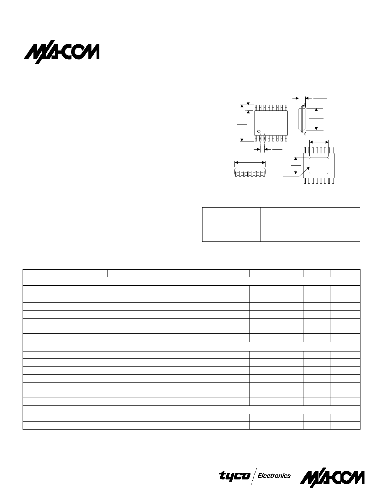
Exposed
Pad
1
.118
.041/.031
1,05/,80
.177/.169
4,5/4,3
.118
3,0
3,0
TSSOP-16 Plastic Package
(.039)
Pin 16
.252
6,4
Pin 1
.201/.193
5,1/4,9
1. Dimensions are: in / mm
.0256
0,65
Ordering Information
Part Number Package
MD59-0022TR Forward Tape and Reel
MD59-0022RTR Reverse Tape and Reel
MD59-0022SMB Sample Board
1. If specific reel size is required, consult factory for part number assignment.
1
1
Electrical Specifications TA = 25°C, VDD = 3.0V
Parameter Test Conditions Units Min. Typ. Max.
Complete Upconverter1 / High Power Mode
Conversion Gain V
CDMA Linear Output Power
Noise Figure LO Frequency = 1580 - 1780 MHz dB 10
I
DD
VSWR (All Ports) IF = 130 MHz 1.5:1
IF Input Impedance Ohms 265
LO-to-RF Port Leakage dBm -18
Complete UPconverter1 / Low Power Mode
Conversion Gain V
CDMA Linear Output Power
Noise Figure LO Frequency = 1580 = 1780 MHz dB 10
I
DD
VSWR (All Ports) IF = 130 MHz 1.5:1
IF Input Impedance Ohms 265
LO-to-RF Port Leakage dBm -18
RF Driver Amplifier
Gain V
Gain V
1. Complete upconverter / driver measurements taken with a surface mount SAW filter between Mixer Ouput and Driver Input.
2. CDMA Linear power is defined as 51 dBc ACPR at a 1.228 MHz Offset from the carrier frequency.
2
2
= VDD dB 24 27.2
CTRL
RF Frequency = 1710 - 1910 MHz dBm 9
LO Power = -10 dBm mA 66
= (0V) dB 22
CTRL
RF Frequency = 1710 - 1910 MHz dBm 2
LO Power = -10 dBm mA 46
= VDD, RF Frequency = 1710 - 1910 MH z dB TBD
CTRL
= 0V, RF Frequency = 1710 - 1910 MHz dB TBD
CTRL
Specifications subject to change without notice.
V 2.0
North America: Tel. (800) 366-2266, Fax (800) 618-8883
Asia/Pacific: Tel.+81-44-844-8296, Fax +81-44-844-8298
Europe: Tel. +44 (1344) 869 595, Fax+44 (1344) 300 020
Visit www.macom.com for additional data sheets and product information.
PCS CDMA Upconverter / Driver 1710—1910 GHz
MD59-0022
Pin Configuration
PIN No. PIN Description
1 DRV VDD1 Driver Amplifier first stage supply voltage. Must be RF
2 DRV In
3 GND DC and RF Ground
4 GND DC and RF Ground
5 MIX OUT
6 GND DC and RF Ground
7 LO IN Local Oscillator Input (-10 to -5 dBm) (DC blocked)
8 LO VDD LO Amplifier Supply Voltage - Bypassing required
9 IF+ VDD IF+ supply voltage. Off chip inductor and IF bypassing
10 IF+ IN IF+ input port. Off chip matching elements required
11 IF- IN
IF- V
12 IF- VDD IF- supply voltage. Off chip induct or and IF bypassing
13 GND DC and RF Gr ound
14 DRV VDD2 Driver amplifier second stage supply voltage. Must be
15 DRV OUT
16 DRV SRC Source bias voltage of driver output stage. Required RF
bypassed
50 Ω Input to driver amplifier (DC blocking required)
50 Ω Output of Mixer (DC block ed )
required
IF- input port. Off chip matching elements required
DD
required
RF bypassed
50 Ω output of Driver Amplifi er (D C bl o ck ed inte rn ally)
bypassing and may be use d to control ouput stage
current
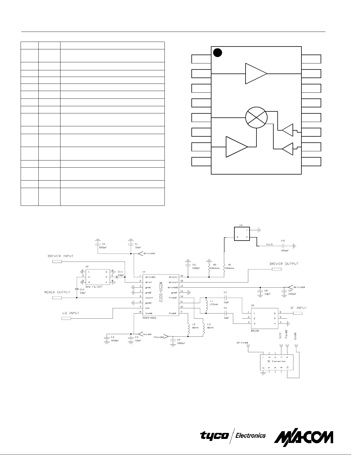
Block Diagrams
DRV VDD1
DRV IN
GND
GND
MIX OUT
GND
LO IN
LO V
DD
DRV SRC
DRV OUT
DRV V
DD
GND
IF- V
IF- IN
IF+ IN
IF+ V
2
DD
DD
Sample Board Schematic
DTC114 YE TL
if- in
if+ in
J1
1. Saw filter characterist ic s t o be determ i ned by cust omer, dependi ng on band of operat i on. Sample boards are supplied without saw filter in stalled.
Data supplied with sample board is measured over US PCS1900 Tx Bond using external K&L BPF (p/n SB121-1850/T450-0/OP) and 2 dB attenuation to emulate typical saw filter characteristics.
Specifications subject to change without notice.
North America: Tel. (800) 366-2266, Fax (800) 618-8883
Asia/Pacific: Tel.+81-44-844-8296, Fax +81-44-844-8298
Europe: Tel. +44 (1344) 869 595, Fax+44 (1344) 300 020
Visit www.macom.com for additional data sheets and product information.
V 2.0

PCS CDMA Upconverter / Driver 1710—1910 GHz
MD59-0022
External Circuitry Parts List
Ref. Designation Value Purpose
C1, C3 C8 33 pF RF Bypass
C2, C4, C5, C9,
C10, C11, C12, C13
C6, C7 10 pF IF Matching
L1 270 nH IF Matching
L2, L3 82 nH RF Choke
R1
R2
U1 MD59-0022 Upconverter / Driver
U2 Filter LO and Image signals
U3 E Series
U4 DCT114Y
J1 DC
1000 pF RF / IF Bypass
18 Ω
68 Ω
XFMR
ETL
Connect
Source Bias Resistor
Source Bias Resistor for low
current mode
5:1 Transformer for IF matching
Bipolar transistor for current
switching (ROHM)
10 PIN DC Connector
Operating Instructions
The MD59-0022 is a highly integrated MMIC upconverter/driver
for the 1710-1910 MHz PCS band. The upconverter/driver provides
exceptional RF performance while consuming low DC current and
is packaged in a low cost plastic package. It i s ideal for light weigh t
battery operated portable radio systems.
The transmit chain consists of a balanced IF amplifier, balanced
mixer with single-ended RF output and a two stage RF driver
amplifier as shown in the block diagram on the previous page.
Surface mount resistors, inductors and capacitors are used in
conjunction with the IC for an optimum performance, tunability
and ease of use. A schematic, showing the IC and required external
components, is shown on page 2.
An external self-bias resistor R1, which is RF bypassed, allows the
current in the driver amplifier to be varied to obtain the required
linear output power. By placing a bipolar transistor in series with
the self-bias resistor, as shown in the schematic, the current
consumption in the driver can be dynamically switched to provide a
high and low power mode of operation. In high power mode, the
bipolar transistor is on and the driver output stage is self-biased
through R1 to provide +9 dBm of linear output power. By switching
off the transistor, the output stage is biased through the higher
resistance R2 thus reducing the current by ~25 mA to give 2 dBm
of linear output power. The dual bipolar (U4) shown in the
assembly drawing may be replaced by a smaller single transistor
package with similar performance .
An external filter is required between the mixer output and driver
amplifier input to reduce the amplitude of the image and local
oscillator signals coming out of the mixer. This filter should have a
50 Ω input and output impedance. The mixer is a balanced resistive
FET mixer which provides exceptional linearity and isolation with
low loss and no DC current.
Recommended PCB Configuration
Cross Section View
RF Traces +
Components
RF
Ground
DC
Routing
Customer
The IFA input ports are externally matched to 265 Ω differential
impedance using two off chip capacitors and an off chip inductor.
This allows maximum flexibility of intermediate frequency and IF
filter. The IFA output ports are matched to the mixer using off chip
inductors, which are also used for DC bias injection. A matching
network such as that shown below can be used to match both the
input and output of the IFA at the required frequency. The inductor
also acts as a choke for the DC suppl y lin e.
The LO input port is internally matched to 50 Ω. A LO buffer
amplifier amplifies the -10 dBm input signal to the level required to
drive the mixer. Performance can be enhanced slightly with a drive
level of -5 dBm.
All DC supply lines must be properly bypassed at RF frequencies to
obtain optimum performance and at lower frequency to maintain
unconditional stability. Capacitors C1, C3 and C8 are RF bypass
capacitors for the LO amplifier and the driver amplifier. The value
and placement of these capacitors are critical in determining the
frequency response of these amplifiers. Capacitor C11 is a source
bypass capacitor for the second stage of the driver amplifier. The
placement of this capacitor will affect the gain of the amplifier. For
best performance, all the RF bypass capacitors should be placed as
shown in the recommended PCB diagram shown above. Capacitors
C2, C4, C5 and C9 are 1000 pF low frequency DC supply bypass
capacitors. Their value and placement are less critical than the
other capacitors. However, for best results, these cap acitors should
be located as close to the package leads as possible.
Specifications subject to change without notice.
North America: Tel. (800) 366-2266, Fax (800) 618-8883
Asia/Pacific: Tel.+81-44-844-8296, Fax +81-44-844-8298
Europe: Tel. +44 (1344) 869 595, Fax+44 (1344) 300 020
Visit www.macom.com for additional data sheets and product information.
V 2.0

PCS CDMA Upconverter / Driver 1710—1910 GHz
Typical Performance Curves
Korean PCS Band US PCS Band
Conversion Gain vs. Frequency
LO = -10dBm, -5 dBm, V
28
27
26
High Power Mode
25
24
23
22
GAIN (dB)
21
20
19
18
1.74 1.75 1.76 1.77 1.78 1.79
-5dBm
-10dBm
RF FREQUENCY (GHz)
= 3.0V
DD
-5dBm
-10dBm
Low Power Mode
Conversion Gain vs. Frequency
LO = -10 dBm, -5 dBm, VDD = 3.0V
26
High Power Mode
25
24
23
22
21
GAIN (dB)
20
19
18
1.83 1.84 1.85 1.86 1.87 1.88 1.89 1.9 1.91 1.92 1.93
MD59-0022
-5dBm
-10dBm
-5dBm
-10dBm
Low P ower Mode
RF FREQUENCY (GHz)
Conversion Gain vs. Frequency
= 2.8V, 3.0V, 3.3V, LO = -10dBm
V
DD
28
27
26
25
24
23
22
GAIN (dB)
21
20
19
18
1.74 1.75 1.76 1.77 1.78 1.79
High Power Mode
3.3V
RF FREQUENCY (GHz)
2.8V
Low P ower Mode
3.0V
2.8V
3.3V
3.0V
LO-to-RF Leakage vs. Frequency
LO = -10dBm, -5 dBm, V
-20
-22
-24
-26
-28
-30
-32
-34
-36
LO LEAKAGE (dBm)
-38
-40
1.74 1.75 1.76 1.77 1.78 1.79
RF FREQUENCY (GHz)
-5dBm
-10dBm
= 3.0V
DD
LO-to-RF Leakage vs. Frequency
-10dBm
= 3.0V
DD
LO = -10dBm, -5 dBm, V
-20
-22
-24
-26
-28
-30
-32
-34
-36
LO LEAKAGE (dBm)
-38
-40
1.83 1.84 1.85 1.86 1.87 1.88 1.89 1.9 1.91 1.92 1.93
-5dBm
RF FREQUENCY (GHz)
Specifications subject to change without notice.
North America: Tel. (800) 366-2266, Fax (800) 618-8883
Asia/Pacific: Tel.+81-44-844-8296, Fax +81-44-844-8298
Europe: Tel. +44 (1344) 869 595, Fax+44 (1344) 300 020
Visit www.macom.com for additional data sheets and product information.
V 2.0

PCS CDMA Upconverter / Driver 1710—1910 GHz
Typical Performance Curves (Cont’d)
MD59-0022
ACPR vs. Output Power
LO = -10dBm, -5 dBm, VDD = 3.0V
70
68
66
Low Power Mode
64
62
60
58
56
ACPR (dBc)
54
52
50
48
-4 -2 0 2 4 6 8 10 12
-10dBm
-5dBm
P
OUT
High Power Mode
-5dBm
-10dBm
(dBm)
Lo Input Return Loss vs. Frequency
LO = -10dBm, V
10
5
0
-5
-10
-15
-20
-25
RETURN LOSS (dB)
-30
-35
-40
1.41.451.51.551.61.651.71.751.81.851.9
= 3.0V
DD
LO FREQUENCY (GHz)
ACPR vs. Output Power
VDD = 2.8V, 3.0V, 3.3V, LO = -10dBm
70
68
66
Low Power Mode
64
62
60
58
56
ACPR (dBc)
54
52
50
48
-4 -2 0 2 4 6 8 10 12
3.0V
2.8V
3.3V
P
High Power Mode
(dBm)
OUT
3.3V
3.0V
2.8V
IF Input Return Loss vs. Frequency
LO = -5 dBm, VDD = 3.0V
10
5
0
-5
-10
-15
-20
-25
RETURN LOSS (dB)
-30
-35
-40
0 0.02 0.04 0.06 0.08 0.1 0.12 0.14 0.16 0.18 0.2
IF FREQUENC Y ( GHz)
IF Input Return Loss vs. Frequency
LO = -5 dBm, V
10
5
0
-5
-10
-15
-20
RETURN LOSS (dB)
-25
-30
-35
-40
1.6 1.65 1.7 1.75 1.8 1.85 1.9 1.95 2 2.05 2.1
= 3.0V
DD
RF FREQUENCY (GHz)
Driver Input Return Loss vs. Frequency
High and Low Power Mode, V
10
5
0
-5
-10
-15
-20
-25
RETURN LOSS (dB)
-30
-35
-40
1.6 1.65 1.7 1.75 1.8 1.85 1.9 1.95 2 2.05 2.1
RF FREQUENCY (GHz)
= 3.0V
DD
Driver Output Return Loss vs. Frequency
High and Low Power Mode, V
10
5
0
High Power Mode
-5
-10
-15
-20
-25
RETURN LOSS (dB)
-30
-35
-40
1.6 1.65 1.7 1.75 1.8 1.85 1.9 1.95 2 2.05 2.1
Low Power Mode
RF FREQUENY (GHz)
= 3.0V
DD
Specifications subject to change without notice.
North America: Tel. (800) 366-2266, Fax (800) 618-8883
Asia/Pacific: Tel.+81-44-844-8296, Fax +81-44-844-8298
Europe: Tel. +44 (1344) 869 595, Fax+44 (1344) 300 020
Visit www.macom.com for additional data sheets and product information.
V 2.0
 Loading...