

Page 1
MCP8063
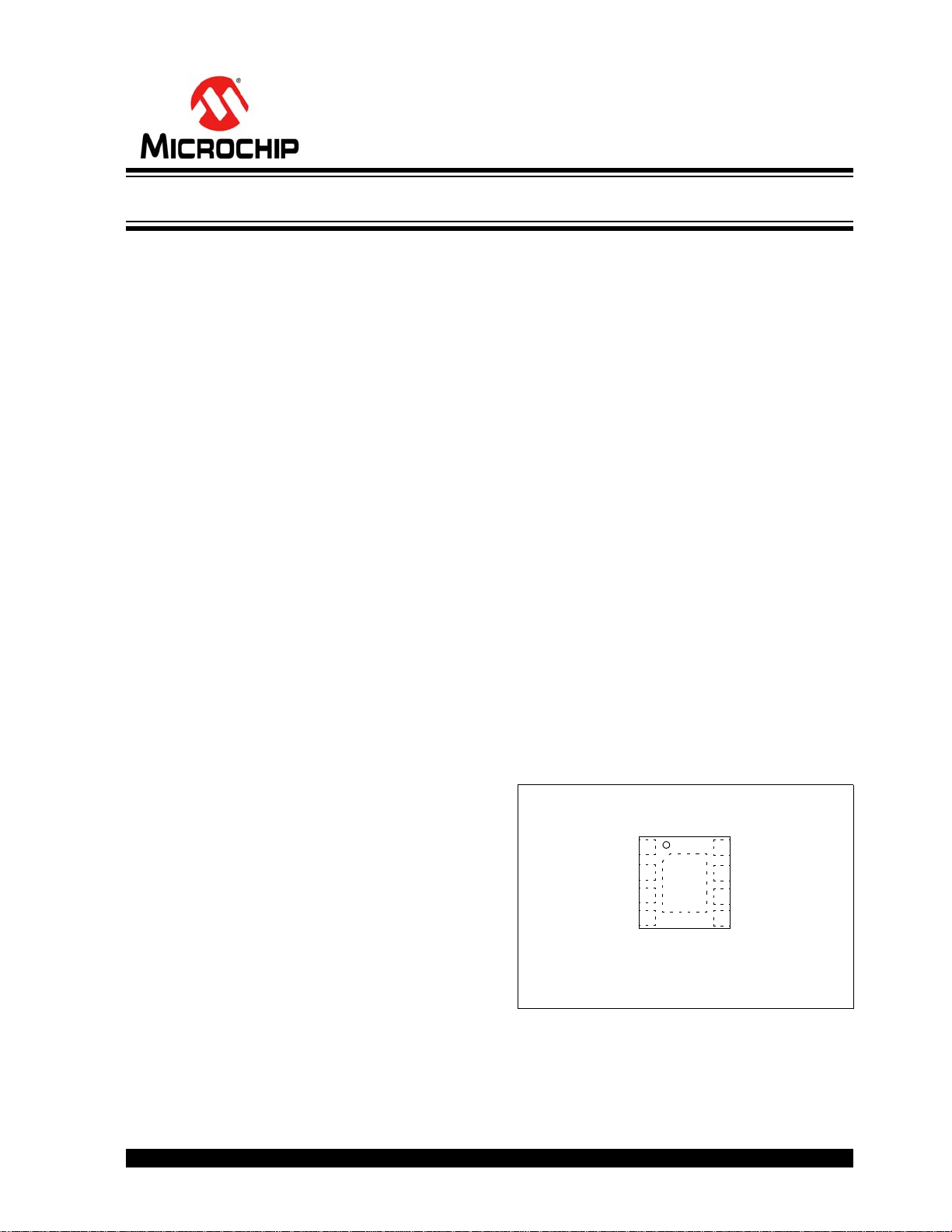
4x4 DFN*
* Includes Exposed Thermal Pad (EP); see Ta bl e 3 -1 .
Top V i ew
OUT1
V
BIAS
OUT2
V
DD
OUT3
1
2
3
4
8
7
6
5
GND
PWMFG
EP
9
MCP8063
3-Phase Brushless Sinusoidal Sensorless Motor Driver
Features
• Automotive AEC-Q100 Qualified, PPAP available
upon request
• Position Sensorless BLDC Drivers (no Hall
Sensor required)
• 180° Sinusoidal Drive for High Efficiency and Low
Acoustic Noise
• Supports 2V to 14V Power Supplies
• Speed Control through Power Supply Modulation
(PSM) and/or Pulse-Width Modulation (PWM)
• Built-In Frequency Generator (FG output signal)
• Built-In Lock-Up Protection and Automatic
Recovery Circuit (external capacitor not
necessary)
• Built-In Overcurrent Limitation (1.5A)
• Built-In Overvoltage Protection
• Built-In Thermal Shutdown Protection
• Thermally Enhanced 8-Lead 4 mm x 4 mm DFN
Package with Exposed Pad
• 23 kHz PWM Output Frequency
• No External Tuning Required
• Optimized for Fan Cooling Systems
Typical Applications
• Silent Notebook CPU/GPU Cooling Fans
• Air Ventilation System
• 12V 3-Phase BLDC Motors
Description
The MCP8063 device is a highly integrated 3-phase,
full-wave sensorless driver for brushless motors. It
features a 180° sinusoidal drive, high torque output,
and silent drive. Its integrated features and the wide
power supply range (2V to 14V) make the MCP8063 an
ideal candidate for a broad range of motor
characteristics, requiring no external tuning. Speed
control can be achieved through either power supply
modulation (PSM) or pulse-width modulation (PWM).
Due to the compact packaging and minimum bill of
materials (power transistors integrated, no Hall sensor,
no external tuning), the MCP8063 is optimized for fan
applications that require high efficiency and low
acoustic noise at competitive costs. Frequency
generator output enables precision speed control in
closed-loop applications. The MCP8063 driver
includes a Lock-Up Protection mode, which turns off
the output current when the motor is under lock
condition, and an automatic recovery that enables the
fan to restart when the lock condition is removed.
Features such as motor overcurrent limitation and
thermal shutdown protection improve motor system
reliability without additional efforts from design
engineers.
The MCP8063 is available in a compact
thermally-enhanced 8-lead 4 mm x 4 mm DFN
package with exposed pad.
Package Types
2014 Microchip Technology Inc. DS20005257B-page 1
Page 2
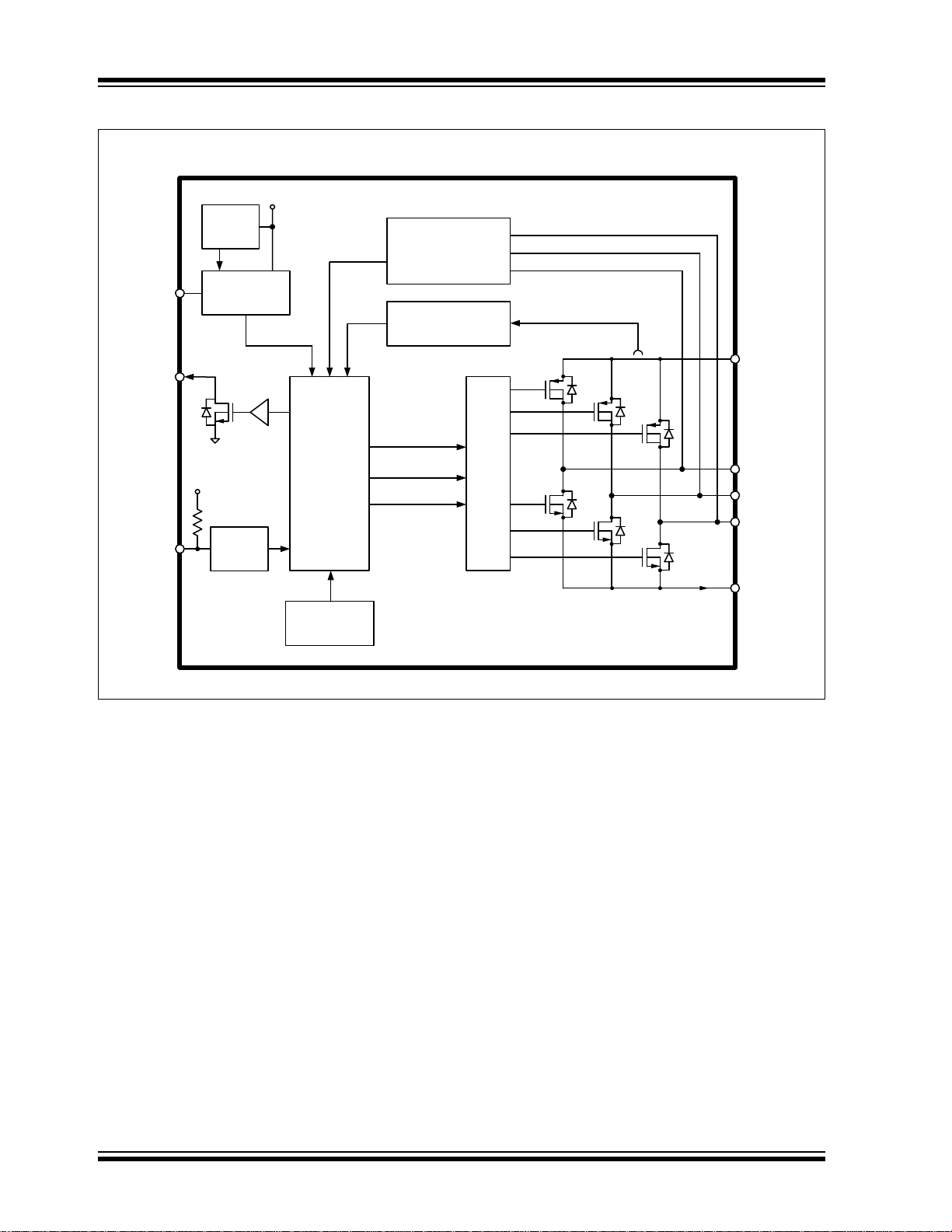
MCP8063
Thermal
Protection
V
BIA S
OUT1
OUT2
MCU
PWM
FG
OUT3
V
DD
Output Drive Circu it
Motor Phase
Detection Circuit
Overcurrent
Limitation
PWM
Input
V
DD
Regulator
V
REF
GND
V
BIA S
Functional Block Diagram
DS20005257B-page 2 2014 Microchip Technology Inc.
Page 3
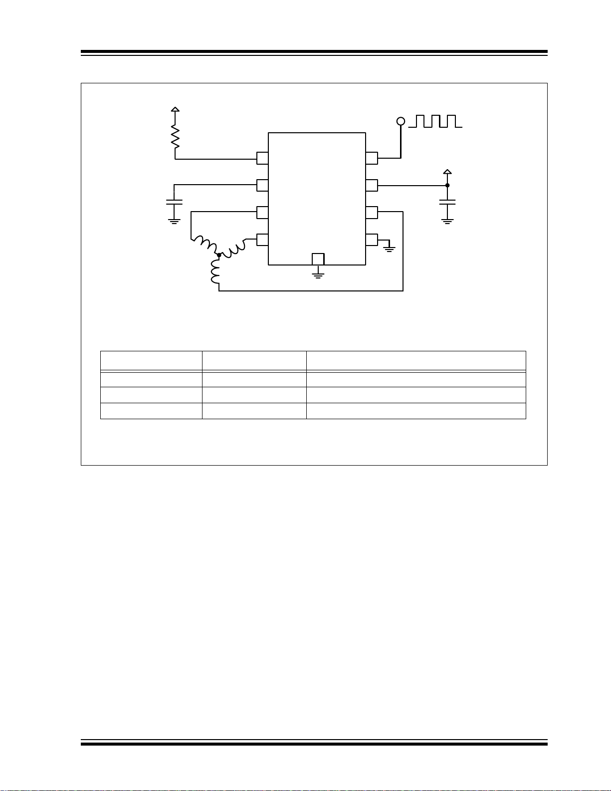
Typical Application – Fan Motor Driver Using the MCP8063
Recommended External Components for Typical Application
Element Type/Value Comment
C
1
≥1 µF Connect as close as possible to IC input pins
C
2
≥10 µF Connect as close as possible to IC input pins
R
1
≥10 kΩ Connect to V
logic
on controller side
OUT1
FG
V
BIA S
OUT2 GND
V
DD
PWM
OUT3
1
2
3
45
6
7
8
MCP8063
V
DD
PWM Input
(0.02-100 kHz)
C
1
C
2
R
1
V
LOGIC
(Controller Side)
9
EP
MCP8063
2014 Microchip Technology Inc. DS20005257B-page 3
Page 4

MCP8063
1.0 ELECTRICAL CHARACTERISTICS
† Notice: Stresses above those listed under “Maximum
Ratings” may cause permanent damage to the device.
This is a stress rating only and functional operation of
the device at those or any other conditions above those
Absolute Maximum Ratings†
Power Supply Voltage (V
Maximum OUT1,2,3 Voltage (V
Maximum Output Current
FG Maximum Output Voltage (V
FG Maximum Output Current (I
Maximum Voltage (V
V
BIAS
PWM Maximum Voltage (V
Maximum Junction Temperature (T
HBM ESD protection on all pins.......................................4 kV
) .................... -0.7 to +16.0V
DD_MAX
(1)
(I
OUT_MAX
BIAS_MAX
PWM_MAX
OUT_MAX
FG_MAX
) ........ -0.7 to +16.0V
) ...........-1.7A to +1.7A
) ......... -0.7 to +16.0V
FG_MAX
) .....................5.0 mA
) ................ -0.7 to +4.0V
) ................ -0.7 to +4.0V
)..........................+150°C
J
indicated in the operational listings of this specification
is not implied. Exposure to maximum rating conditions
for extended periods may affect device reliability.
Note 1: OUT1, OUT2, OUT3 (Continuous,
100% duty cycle).
ELECTRICAL CHARACTERISTICS
Electrical Specifications: Unless otherwise specified, all limits are established for V
Temperature = +25°C.
Parameters Sym. Min. Typ. Max. Units Conditions
Power Supply Voltage V
Power Supply Current I
OUT1/2/3
R
DD
VDD
ON(H)
2—14V
—
—
10 —
5 Lock-Protection Mode
—
mAmARotation Mode
—0.6 1 Ω I
High Resistance
OUT1/2/3
R
ON(L)
—0.6 1 Ω I
Low Resistance
OUT1/2/3
R
ON(H+L)
—1.2 2 Ω I
Total Resistance
OUT1/2/3 Maximum
I
OUT_LIM
1.4 1.5 1.6 A Note 1
Current Limitation
V
Output Voltage V
BIAS
PWM Input Frequency f
PWM Input H Level V
PWM Input L Level V
PWM Internal Pull-Up
Current
PWM Output
BIAS
PWM
PWM_H
PWM_L
I
PWM_L
f
PWM_O
—
—
3——VVDD= 3.3V to 14V
VDD–0.2 V VDD<3.3V
0.02 — 100 kHz
0.8 × V
BIAS
0—
—3.6V
0.2 × V
BIAS
V
17 34 — µA PWM = GND, VDD= 3.3V to 14V
8 17 — µA PWM = GND, V
—23—kHz
Frequency
FG Output Pin Low
V
OL_FG
— — 0.25 V IFG=-1 mA
Level Voltage
FG Output Pin Leakage
I
LH_FG
——10µAV
Current
Lock Protection
T
RUN
—0.5— s
Operating Time
Lock Protection
T
WAIT
4.0 4.5 5.0 s
Waiting Time
Note 1: Minimum and maximum parameter is not production tested and is specified by design and validation.
Reference PCB, according to JEDEC standard EIA/JESD 51-9.
= 12.0V,
DD
=0.5A, VDD= 3.3V to 14V
OUT
(Note 1)
= -0.5A, VDD= 3.3V to 14V
OUT
(Note 1)
=0.5A, VDD= 3.3V to 14V
OUT
(Note 1)
<3.3V
DD
=14V
FG
DS20005257B-page 4 2014 Microchip Technology Inc.
Page 5
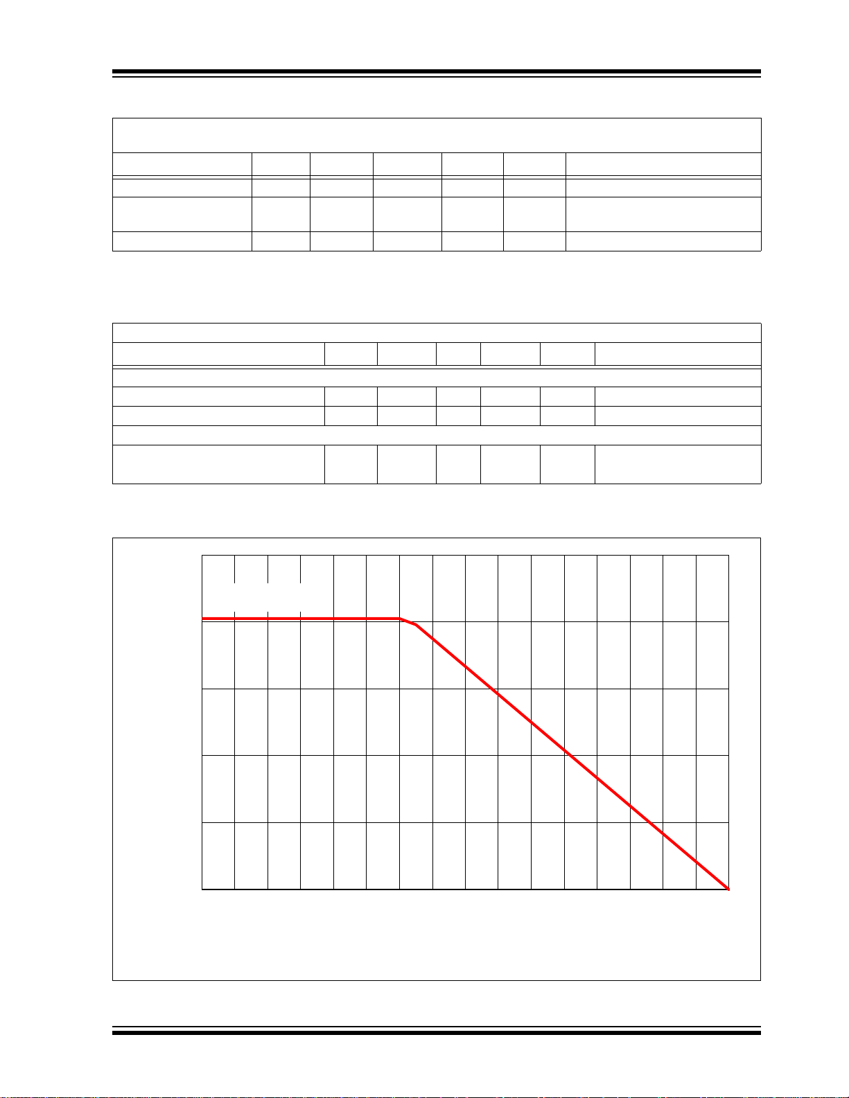
MCP8063
0
0.5
1
1.5
2
2.5
-10
0
10
20
30
40
50
60
70
80
90
100
110
120
130
140
150
P
DMAX
(W)
DFN-8
ELECTRICAL CHARACTERISTICS (CONTINUED)
Electrical Specifications: Unless otherwise specified, all limits are established for V
Temperature = +25°C.
Parameters Sym. Min. Typ. Max. Units Conditions
Thermal Shutdown T
Thermal Shutdown
Hysteresis
Input Over Voltage V
Note 1: Minimum and maximum parameter is not production tested and is specified by design and validation.
Reference PCB, according to JEDEC standard EIA/JESD 51-9.
T
SD_HYS
SD
OV
— 170 — °C
—25—°C
—18.5— V
TEMPERATURE SPECIFICATIONS
Electrical Specifications: Unless otherwise specified, all limits are established for V
Parameters Sym. Min. Typ. Max. Units Conditions
Temperature Ranges
Operating Temperature T
Storage Temperature Range T
Package Thermal Resistances
Thermal Resistance, 8LD 4x4 DFN
Note 1: Minimum and maximum parameter is not production tested and is specified by design and validation.
Derating applies for ambient temperatures outside the specified operating range (refer to Figure 1-1).
OPR
STG
JA
JC
-40 — +125 °C
-55 — +150 °C
—48—°C/W
—7—°C/W
= 12.0V,
DD
= 12.0V, TA=+25°C.
DD
TA(°C)
FIGURE 1-1: Allowable Power Dissipation (P
) as a Function of Ambient Temperature (TA).
D_MAX
2014 Microchip Technology Inc. DS20005257B-page 5
Page 6

MCP8063
-2
0
2
4
6
8
10
12
14
16
-40 -25 -10 5 20 35 50 65 80 95 110 125
(%)
VDD= 2V
0
0.5
1
1.5
2
2.5
3
3.5
-40 -25 -10 5 20 35 50 65 80 95 110 125
BIAS
VDD= 2V
VDD= 3.3V
VDD= 14V
25
30
35
40
45
-40 -25 -10 5 20 35 50 65 80 95 110 125
IL
BIAS
VDD= 14V
VDD= 2V
50
55
60
65
70
-40 -25 -10 5 20 35 50 65 80 95 110 125
IH
BIAS
VDD= 14V
VDD= 2V
0
0.1
0.2
0.3
0.4
0.5
0.6
0.7
0.8
0.9
1
-40 -25 -10 5 20 35 50 65 80 95 110 125
ON
R
ON(H)
R
ON(L)
6.6
6.8
7
7.2
7.4
7.6
7.8
8
8.2
-40 -25 -10 5 20 35 50 65 80 95 110 125
I
VDD
Current (mA)
VDD= 14V
2.0 TYPICAL PERFORMANCE CURVES
Note: The graphs and tables provided following this note are a statistical summary based on a limited number of
samples and are provided for informational purposes only. The performance characteristics listed herein
are not tested or guaranteed. In some graphs or tables, the data presented may be outside the specified
operating range (e.g., outside specified power supply range) and therefore outside the warranted range.
Note: Unless otherwise indicated, T
Oscillator Frequency Deviation
Temperature (C°)
=+25°C, VDD= 14V, OUT1, 2, 3 and PWM open.
A
V
= 14V
FIGURE 2-1: Oscillator Frequency Deviation vs. Temperature.
(V)
V
75
)
(% of V
PWM V
Temperature (C°)
FIGURE 2-4: Input (PWM) V
Temperature.
(ȍ)
R
IH
vs.
FIGURE 2-2: Internal Regulated Voltage
(V
) vs. Temperature.
BIAS
50
)
(% of V
PWM V
FIGURE 2-3: Input (PWM) V
Temperature.
DS20005257B-page 6 2014 Microchip Technology Inc.
Temperature (C°)
Temperature (C°)
IL
vs.
Temperature (C°)
FIGURE 2-5: Output R
Temperature (V
=3.3V).
DD
Temperature (C°)
Resistance vs.
ON
FIGURE 2-6: Supply Current vs. Temperature.
Page 7

MCP8063
0.04
0.05
0.06
0.07
0.08
0.09
0.1
0.11
0.12
-40 -25 -10 5 20 35 50 65 80 95 110 125
VDD= 3.3V
VDD= 2V
-40
-35
-30
-25
-20
-15
-10
-5
0
-40 -25 -10 5 20 35 50 65 80 95 110 125
VDD= 2V
VDD= 14V
Note: Unless otherwise indicated, T
FG Pin Drive (V)
Temperature (C°)
=+25°C, VDD= 14V, OUT1, 2, 3 and PWM open.
A
FIGURE 2-7: FG Output Pin Low Level
Voltage (I
=-1mA).
FG
FIGURE 2-10: Typical Outputs on Closed Loop.
PWM Pull-Up Current (µA)
FIGURE 2-8: PWM Pull-Up Current vs. Temperature.
FIGURE 2-9: Typical Output on Start-Up.
2014 Microchip Technology Inc. DS20005257B-page 7
Temperature (C°)
FIGURE 2-11: Typical Ro t o r L oc k S it u ati o n.
Page 8

MCP8063
3.0 PIN DESCRIPTIONS
The descriptions of the pins are listed in Ta bl e 3- 1.
TABLE 3-1: MCP8063 PIN FUNCTION TABLE
MCP8063
4x4 DFN
1 FG O Motor Speed Indication Output Pin
2V
3 OUT1 O Single-Phase Coil Output Pin
4 OUT2 O Single-Phase Coil Output Pin
5 GND P Negative Voltage Supply Pin (Ground)
6 OUT3 O Single-Phase Coil Output Pin
7V
8 PWM I PWM Input Signal for Speed Control Pin
9 EP P Exposed pad is used for thermal dissipation. Connect to GND.
Legend: I = Input; O = Output; P = Power
Symbol Type Description
BIAS
DD
P Internal Regulator Output Pin (for decoupling only)
P Positive Voltage Supply for Motor Driver Pin
DS20005257B-page 8 2014 Microchip Technology Inc.
Page 9

MCP8063
FG 720
PS
-----------------------
Where:
P=
Total number of poles in the motor
S=Total number of slots in the motor
= Rotor speed RPM
+145°C
+170°C
4.0 FUNCTIONAL DESCRIPTION
The MCP8063 device generates a full-wave signal to
drive a 3-phase sensorless BLDC motor. High
efficiency and low power consumption are achieved
due to DMOS transistors and synchronous rectification
drive type. The current carrying order of the output is as
follows: OUT1 OUT2 OUT3.
4.1 Speed Control
The rotational speed of the motor can be controlled
either through the PWM digital input signal or by
varying the power supply (V
is “High” (or left open), the motor rotates at full speed.
When the PWM signal is “Low”, the motor is stopped
(and the driver outputs are set to high impedance). By
changing the PWM duty cycle, the speed can be
adjusted. Notice that the PWM frequency has no
special meaning for the motor speed and is
asynchronous with the activation of the output
transistors. Thus, the user has maximum freedom to
choose the PWM system frequency within a wide range
(from 20 Hz to 100 kHz), while the output transistor
activation always occurs at a fixed rate, which is
outside the range of audible frequencies. The typical
output frequency of MCP8063 is 23 kHz.
4.2 Frequency Generator Function
The Frequency Generator output is a “Hall-sensor
equivalent” digital output, giving information to an
external controller about the speed and phase of the
motor. The FG pin is an open-drain output, connecting
to a logical voltage level through an external pull-up
resistor. When a lock (or out-of-sync) situation is
detected by the driver, this output is set to high
impedance until the motor is restarted. Leave the pin
open when not used. The FG signal can be used to
compute the motor speed in rotations per minute
(RPM). Typically, for a four-pole BLDC fan (4P/6S), the
speed in RPMs is 30 x FG frequency (Hz).
). When the PWM signal
DD
4.3 Lock-Up Protection and Automatic Restart
If the motor is stopped (blocked) or if it loses
synchronization with the driver, a lock-up protection
circuit detects this situation and ties the outputs to GND
in order to dissipate the remaining energy from the
rotor with a minimum of self heating. After a “waiting
time” (T
normal operation resumes for a given time (T
case the motor is still blocked, a new period of waiting
time is started. T
internally, so that no external capacitor is needed.
), the lock-up protection is released and
WAIT
WAIT
and T
timings are fixed
RUN
RUN
). In
4.4 Overcurrent Limitation
The motor peak current is limited by the driver to a fixed
value (defined internally), thus limiting the maximum
power dissipation in the coils.
4.5 Thermal Shutdown
The MCP8063 device has a thermal protection function
which detects when the die temperature exceeds
TSD= +170°C. When this temperature is reached, the
circuit enters Thermal Shutdown mode and the outputs
OUT1, OUT2 and OUT3 are tied to GND in order to
dissipate the remaining energy from the rotor with a
minimum of self-heating. Once the junction
temperature (T
normal operation resumes (the thermal detection
circuit has +25°C hysteresis function).
Normal operation
) has dropped below +145°C, the
SD
Thermal Shutdown
T
SD
EQUATION 1-1:
2014 Microchip Technology Inc. DS20005257B-page 9
FIGURE 4-1: Thermal Protection Hysteresis.
4.6 Internal Voltage Regulator
V
voltage is generated internally and is used to
BIAS
supply internal logical blocks. The V
connect an external decoupling capacitor (1 µF or
higher). Notice that this pin is for IC internal use and is
not designed to supply DC current to external blocks.
pin is used to
BIAS
4.7 Overvoltage Shutdown
The MCP8063 device has an overvoltage protection
function which detects when the V
V
= +18.5V. When this temperature is reached, the
OV
circuit enters Thermal Shutdown mode, and outputs
OUT1, OUT2 and OUT3 are disabled (high impedance).
voltage exceeds
DD
Page 10

MCP8063
Legend: XX...X Customer-specific information
Y Year code (last digit of calendar year)
YY Year code (last 2 digits of calendar year)
WW Week code (week of January 1 is week ‘01’)
NNN Alphanumeric traceability code
Pb-free JEDEC
®
designator for Matte Tin (Sn)
* This package is Pb-free. The Pb-free JEDEC designator ( )
can be found on the outer packaging for this package.
Note: In the event the full Microchip part number cannot be marked on one line, it will
be carried over to the next line, thus limiting the number of available
characters for customer-specific information.
3
e
8-Lead DFN (4x4x0.9 mm) Example
YYWW
NNN
XXXXXX
XXXXXX
PIN 1
PIN 1
8063
300EMD
1442
256
5.0 PACKAGING INFORMATION
5.1 Package Marking Information
3
e
DS20005257B-page 10 2014 Microchip Technology Inc.
Page 11

8-Lead Plastic Dual Flat, No Lead Package (MD) – 4x4x0.9 mm Body [DFN]
Note: For the most current package drawings, please see the Microchip Packaging Specification located at
http://www.microchip.com/packaging
Microchip Technology Drawing C04-131E Sheet 1 of 2
MCP8063
2014 Microchip Technology Inc. DS20005257B-page 11
Page 12

MCP8063
8-Lead Plastic Dual Flat, No Lead Package (MD) – 4x4x0.9 mm Body [DFN]
Note: For the most current package drawings, please see the Microchip Packaging Specification located at
http://www.microchip.com/packaging
Microchip Technology Drawing C04-131E Sheet 2 of 2
DS20005257B-page 12 2014 Microchip Technology Inc.
Page 13

Note: For the most current package drawings, please see the Microchip Packaging Specification located at
http://www.microchip.com/packaging
MCP8063
2014 Microchip Technology Inc. DS20005257B-page 13
Page 14

MCP8063
NOTES:
DS20005257B-page 14 2014 Microchip Technology Inc.
Page 15

APPENDIX A: REVISION HISTORY
Revision B (November 2014)
The following is the list of modifications:
1. Changed FG Maximum Output Voltage values
under Absolute Maximum Ratings† section
2. Changed Power Supply Voltage value under
Absolute Maximum Ratings† section.
3. Added Input Overvoltage Value in Electrical
Characteristics table.
4. Minor typographical corrections.
Revision A (February 2014)
• Original Release of this Document.
MCP8063
2014 Microchip Technology Inc. DS20005257B-page 15
Page 16

MCP8063
NOTES:
DS20005257B-page 16 2014 Microchip Technology Inc.
Page 17

PRODUCT IDENTIFICATION SYSTEM
Device: MCP8063: 3-Phase BLDC Sinusoidal Sensorless Motor Driver
MCP8063T: 3-Phase BLDC Sinusoidal Sensorless Motor Driver
(Tape and Reel)
Temperature
Range:
E = -40°C to +125°C (Extended)
Package: MD =
8-Lead Plastic Dual Flat, No Lead – 4x4x0.9 mm Body (DFN)
Examples:
a) MCP8063-E /MD: E xtended temperature,
8LD 4x4 DFN package
b) MCP8063T-E/MD: Extended temperature,
8LD 4x4 DFN package,
Tape and Reel
PART NO. -X /XX
Package
Tube/Tape and Reel
Device
X
Temperature
Range
To order or obtain information, e.g., on pricing or delivery, refer to the factory or the listed sales office.
MCP8063
2014 Microchip Technology Inc. DS20005257B-page 17
Page 18

MCP8063
NOTES:
DS20005257B-page 18 2014 Microchip Technology Inc.
Page 19

Note the following details of the code protection feature on Microchip devices:
YSTEM
CERTIFIED BY DNV
== ISO/TS 16949 ==
• Microchip products meet the specification contained in their particular Microchip Data Sheet.
• Microchip believes that its family of products is one of the most secure families of its kind on the market today, when used in the
intended manner and under normal conditions.
• There are dishonest and possibly illegal methods used to breach the code protection feature. All of these methods, to our
knowledge, require using the Microchip products in a manner outside the operating specifications contained in Microchip’s Data
Sheets. Most likely, the person doing so is engaged in theft of intellectual property.
• Microchip is willing to work with the customer who is concerned about the integrity of their code.
• Neither Microchip nor any other semiconductor manufacturer can guarantee the security of their code. Code protection does not
mean that we are guaranteeing the product as “unbreakable.”
Code protection is constantly evolving. We at Microchip are committed to continuously improving the code protection features of our
products. Attempts to break Microchip’s code protection feature may be a violation of the Digital Millennium Copyright Act. If such acts
allow unauthorized access to your software or other copyrighted work, you may have a right to sue for relief under that Act.
Information contained in this publication regarding device
applications and the like is provided only for your convenience
and may be superseded by updates. It is your responsibility to
ensure that your application meets with your specifications.
MICROCHIP MAKES NO REPRESENTATIONS OR
WARRANTIES OF ANY KIND WHETHER EXPRESS OR
IMPLIED, WRITTEN OR ORAL, STATUTORY OR
OTHERWISE, RELATED TO THE INFORMATION,
INCLUDING BUT NOT LIMITED TO ITS CONDITION,
QUALITY, PERFORMANCE, MERCHANTABILITY OR
FITNESS FOR PURPOSE. Microchip disclaims all liability
arising from this information and its use. Use of Microchip
devices in life support and/or safety applications is entirely at
the buyer’s risk, and the buyer agrees to defend, indemnify and
hold harmless Microchip from any and all damages, claims,
suits, or expenses resulting from such use. No licenses are
conveyed, implicitly or otherwise, under any Microchip
intellectual property rights.
Trademarks
The Microchip name and logo, the Microchip logo, dsPIC,
FlashFlex, flexPWR, JukeBlox, K
LANCheck, MediaLB, MOST, MOST logo, MPLAB,
OptoLyzer, PIC, PICSTART, PIC
SST, SST Logo, SuperFlash and UNI/O are registered
trademarks of Microchip Technology Incorporated in the
U.S.A. and other countries.
The Embedded Control Solutions Company and mTouch are
registered trademarks of Microchip Technology Incorporated
in the U.S.A.
Analog-for-the-Digital Age, BodyCom, chipKIT, chipKIT logo,
CodeGuard, dsPICDEM, dsPICDEM.net, ECAN, In-Circuit
Serial Programming, ICSP, Inter-Chip Connectivity, KleerNet,
KleerNet logo, MiWi, MPASM, MPF, MPLAB Certified logo,
MPLIB, MPLINK, MultiTRAK, NetDetach, Omniscient Code
Generation, PICDEM, PICDEM.net, PICkit, PICtail,
RightTouch logo, REAL ICE, SQI, Serial Quad I/O, Total
Endurance, TSHARC, USBCheck, VariSense, ViewSpan,
WiperLock, Wireless DNA, and ZENA are trademarks of
Microchip Technology Incorporated in the U.S.A. and other
countries.
SQTP is a service mark of Microchip Technology Incorporated
in the U.S.A.
Silicon Storage Technology is a registered trademark of
Microchip Technology Inc. in other countries.
GestIC is a registered trademarks of Microchip Technology
Germany II GmbH & Co. KG, a subsidiary of Microchip
Technology Inc., in other countries.
All other trademarks mentioned herein are property of their
respective companies.
© 2014, Microchip Technology Incorporated, Printed in the
U.S.A., All Rights Reserved.
ISBN: 978-1-63276-791-2
EELOQ, KEELOQ logo, Kleer,
32
logo, RightTouch, SpyNIC,
QUALITY MANAGEMENT S
2014 Microchip Technology Inc. DS20005257B-page 19
Microchip received ISO/TS-16949:2009 certification for its worldwide
headquarters, design and wafer fabrication facilities in Chandler and
Tempe, Arizona; Gresham, Oregon and design centers in California
and India. The Company’s quality system processes and procedures
are for its PIC
devices, Serial EEPROMs, microperipherals, nonvolatile memory and
analog products. In addition, Microchip’s quality system for the design
and manufacture of development systems is ISO 9001:2000 certified.
®
MCUs and dsPIC® DSCs, KEELOQ
®
code hopping
Page 20

Worldwide Sales and Service
AMERICAS
Corporate Office
2355 West Chandler Blvd.
Chandler, AZ 85224-6199
Tel: 480-792-7200
Fax: 480-792-7277
Technical Support:
http://www.microchip.com/
support
Web Address:
www.microchip.com
Atlanta
Duluth, GA
Tel: 678-957-9614
Fax: 678-957-1455
Austin, TX
Tel: 512-257-3370
Boston
Westborough, MA
Tel: 774-760-0087
Fax: 774-760-0088
Chicago
Itasca, IL
Tel: 630-285-0071
Fax: 630-285-0075
Cleveland
Independence, OH
Tel: 216-447-0464
Fax: 216-447-0643
Dallas
Addison, TX
Tel: 972-818-7423
Fax: 972-818-2924
Detroit
Novi, MI
Tel: 248-848-4000
Houston, TX
Tel: 281-894-5983
Indianapolis
Noblesville, IN
Tel: 317-773-8323
Fax: 317-773-5453
Los Angeles
Mission Viejo, CA
Tel: 949-462-9523
Fax: 949-462-9608
New Yor k , NY
Tel: 631-435-6000
San Jose, CA
Tel: 408-735-9110
Canada - Toronto
Tel: 905-673-0699
Fax: 905-673-6509
ASIA/PACIFIC
Asia Pacific Office
Suites 3707-14, 37th Floor
Tower 6, The Gateway
Harbour City, Kowloon
Hong Kong
Tel: 852-2943-5100
Fax: 852-2401-3431
Australia - Sydney
Tel: 61-2-9868-6733
Fax: 61-2-9868-6755
China - Beijing
Tel: 86-10-8569-7000
Fax: 86-10-8528-2104
China - Chengdu
Tel: 86-28-8665-5511
Fax: 86-28-8665-7889
China - Chongqing
Tel: 86-23-8980-9588
Fax: 86-23-8980-9500
China - Hangzhou
Tel: 86-571-8792-8115
Fax: 86-571-8792-8116
China - Hong Kong SAR
Tel: 852-2943-5100
Fax: 852-2401-3431
China - Nanjing
Tel: 86-25-8473-2460
Fax: 86-25-8473-2470
China - Qingdao
Tel: 86-532-8502-7355
Fax: 86-532-8502-7205
China - Shanghai
Tel: 86-21-5407-5533
Fax: 86-21-5407-5066
China - Shenyang
Tel: 86-24-2334-2829
Fax: 86-24-2334-2393
China - Shenzhen
Tel: 86-755-8864-2200
Fax: 86-755-8203-1760
China - Wuhan
Tel: 86-27-5980-5300
Fax: 86-27-5980-5118
China - Xian
Tel: 86-29-8833-7252
Fax: 86-29-8833-7256
China - Xiamen
Tel: 86-592-2388138
Fax: 86-592-2388130
China - Zhuhai
Tel: 86-756-3210040
Fax: 86-756-3210049
ASIA/PACIFIC
India - Bangalore
Tel: 91-80-3090-4444
Fax: 91-80-3090-4123
India - New Delhi
Tel: 91-11-4160-8631
Fax: 91-11-4160-8632
India - Pune
Tel: 91-20-3019-1500
Japan - Osaka
Tel: 81-6-6152-7160
Fax: 81-6-6152-9310
Japan - Tokyo
Tel: 81-3-6880- 3770
Fax: 81-3-6880-3771
Korea - Daegu
Tel: 82-53-744-4301
Fax: 82-53-744-4302
Korea - Seoul
Tel: 82-2-554-7200
Fax: 82-2-558-5932 or
82-2-558-5934
Malaysia - Kuala Lumpur
Tel: 60-3-6201-9857
Fax: 60-3-6201-9859
Malaysia - Penang
Tel: 60-4-227-8870
Fax: 60-4-227-4068
Philippines - Manila
Tel: 63-2-634-9065
Fax: 63-2-634-9069
Singapore
Tel: 65-6334-8870
Fax: 65-6334-8850
Tai wan - Hsin Chu
Tel: 886-3-5778-366
Fax: 886-3-5770-955
Taiwan - Kaohsiung
Tel: 886-7-213-7830
Taiwan - Taipei
Tel: 886-2-2508-8600
Fax: 886-2-2508-0102
Thailand - Bangkok
Tel: 66-2-694-1351
Fax: 66-2-694-1350
EUROPE
Austria - Wels
Tel: 43-7242-2244-39
Fax: 43-7242-2244-393
Denmark - Copenhagen
Tel: 45-4450-2828
Fax: 45-4485-2829
France - Paris
Tel: 33-1-69-53-63-20
Fax: 33-1-69-30-90-79
Germany - Dusseldorf
Tel: 49-2129-3766400
Germany - Munich
Tel: 49-89-627-144-0
Fax: 49-89-627-144-44
Germany - Pforzheim
Tel: 49-7231-424750
Italy - Milan
Tel: 39-0331-742611
Fax: 39-0331-466781
Italy - Venice
Tel: 39-049-7625286
Netherlands - Drunen
Tel: 31-416-690399
Fax: 31-416-690340
Poland - Wars a w
Tel: 48-22-3325737
Spain - Madrid
Tel: 34-91-708-08-90
Fax: 34-91-708-08-91
Sweden - Stockholm
Tel: 46-8-5090-4654
UK - Wokingham
Tel: 44-118-921-5800
Fax: 44-118-921-5820
03/25/14
DS20005257B-page 20 2014 Microchip Technology Inc.
 Loading...