

Page 1

MCP8025/6
3-Phase Brushless DC (BLDC) Motor Gate Driver with Power Module, Sleep Mode, LIN Transceiver
Features
• AEC-Q100 Grade 0 Qualified
• Quiescent Current:
- Sleep Mode: 5 µA Typical
- Standby Mode: < 200 µA
• LIN Transceiver Interface (MCP8025):
- Compliant with LIN Bus Specifications 1.3,
2.2, and SAE J2602
- Supports baud rates up to 20K baud
- Internal pull-up resistor and diode
- Protected against ground shorts
- Protected against loss of ground
- Automatic thermal shutdown
- LIN Bus dominant timeout
• Three Half-Bridge Drivers Configured to Drive
External High-Side NMOS and Low-Side NMOS
MOSFETs:
- Independent input control for high-side
NMOS and low-side NMOS MOSFETs
- Peak output current: 0.5A @ 12V
- Shoot-through protection
- Overcurrent and short circuit protection
• Adjustable Output Buck Regulator (750 mW)
• Fixed Output Linear Regulators:
- 5V@30mA
-12V@30mA
• Operational Amplifiers:
- one in MCP8025
- three in MCP8026
• Overcurrent Comparator with DAC Reference
• Phase Comparator With Multiplexer (MCP8025)
• Neutral Simulator (MCP8025)
• Level Translators (MCP8026)
• Input Voltage Range: 6V – 40V
• Operational Voltage Range:
-6V–19V (MCP8025)
-6V–28V (MCP8026)
• Buck Regulator Undervoltage Lockout: 4.0V
• Undervoltage Lockout (UVLO): 5.5V (except Buck)
• Overvoltage Lockout (OVLO)
-20V (MCP8025)
-32V (MCP8026)
• Transient (100 ms) Voltage Tolerance: 48V
• Extended Temperature Range (T
• Thermal Shutdown
): -40 to +150°C
A
Applications
• Automotive Fuel, Water, Ventilation Motors
• Home Appliances
• Permanent Magnet Synchronous Motor (PMSM)
Control
• Hobby Aircraft, Boats, Vehicles
Description
The MCP8025/6 devices are 3-phase brushless DC
(BLDC) power modules containing three integrated
half-bridge drivers capable of driving three external
NMOS/NMOS transistor pairs. The three half-bridge
drivers are capable of delivering a peak output current
of 0.5A at 12V for driving high-side and low-side NMOS
MOSFET transistors. The drivers have shoot-through,
overcurrent and short-circuit protection. A Sleep Mode
has been added to achieve a typical “key-off” quiescent
current of 5 µA.
The MCP8025 device integrates a comparator, a buck
voltage regulator, two LDO regulators, power
monitoring comparators, an overtemperature sensor, a
LIN transceiver, a zero-crossing detector, a neutral
simulator and an operational amplifier for motor current
monitoring. The phase comparator and multiplexer
allow for hardware commutation detection. The neutral
simulator allows commutation detection without a
neutral tap in the motor. The buck converter is capable
of delivering 750 mW of power for powering a
companion microcontroller. The buck regulator may be
disabled if not used. The on-board 5V and 12V lowdropout voltage regulators are capable of delivering
30 mA of current.
The MCP8026 replaces the LIN transceiver, neutral
simulator and zero-crossing detector in MCP8025 with
two level shifters and two additional op amps.
The MCP8025/6 operation is specified over a
temperature range of -40°C to +150°C.
Package options include 40-lead 5x5 QFN and 48-lead
7x7 TQFP with Exposed Pad (EP).
2014 Microchip Technology Inc. DS20005339A-page 1
Page 2

MCP8025/6
5mm x 5mm QFN-40
7mm x 7mm TQFP-48
+
EP
41
EP
49
1
2
3
4
5
6
7
8
9
10
11
12
13
14
15
16
171819
20
21
22
23
24
25
26
27
28
29
30
31
32
33
34
35
36
37
38
39
40
1
2
3
4
5
6
7
8
9
10
11
12
131415
16
171819
20
21
222324
36
35
34
33
32
31
30
29
28
27
26
25
484746
45
444342
41
40
393837
PWM2H
PWM1L
PWM1H
CE
LIN_BUS
RX
TX
FAULTn
/TXE
MUX1
MUX2
+12V
V
BA
V
BB
V
BC
PHA
PHB
PHC
HSA
HSB
HSC
ZC_OUT
COMP_REF
ILIMIT_OUT
I_OUT1
I_SENSE1-
I_SENSE1+
P
GND
LSA
LSB
LSC
PWM2L
PWM3H
PWM3L
DE2
CAP1
CAP2
+5VFBVDDLX
PWM2H
PWM1L
PWM1H
CE
LIN_BUS
RX
TX
FAULTn
/TXE
MUX1
MUX2
NC
NC
P
GND
ZC_OUT
COMP_REF
ILIMIT_OUT
I_OUT1
I_SENSE1-
I_SENSE1+
P
GND
LSA
LSB
LSC
P
GND
P
GND
+12V
V
BA
V
BB
V
BC
PHA
PHB
PHC
HSA
HSB
HSC
P
GND
P
GND
PWM2L
PWM3H
PWM3L
DE2
CAP1
CAP2
+5V
FB
VDDLX
V
DD
Package Types – MCP8025
DS20005339A-page 2 2014 Microchip Technology Inc.
Page 3

Package Types – MCP8026
5mm x 5mm QFN-40
7mm x 7mm TQFP-48
EP
41
1
2
3
4
5
6
7
8
9
10
11
12
13
14
15
16
171819
20
21
22
23
24
25
26
27
28
29
30
31
32
33
34
35
36
37
38
39
40
PWM2H
PWM1L
PWM1H
CE
HV_IN1
LV_O UT1
IOUT3
ISENSE3-
ISENSE3+
IOUT2
+12V
V
BA
V
BB
V
BC
PHA
PHB
PHC
HSA
HSB
HSC
ISENSE2-
ISENSE2+
ILIMIT_OUT
I_OUT1
I_SENSE1-
I_SENSE1+
P
GND
LSA
LSB
LSC
PWM2L
PWM3H
PWM3L
DE2
CAP1
CAP2
+5V
FB
VDDLX
+
EP
49
1
2
3
4
5
6
7
8
9
10
11
12
131415
16
171819
20
21
222324
36
35
34
33
32
31
30
29
28
27
26
25
484746
45
444342
41
40
393837
PWM2H
PWM1L
PWM1H
CE
HV_IN1
LV_OUT1
IOUT3
ISENSE3-
ISENSE3+
IOUT2
LV_OUT2
HV_IN2
P
GND
ISENSE2-
ISENSE2+
ILIMIT_OUT
I_OUT1
I_SENSE1-
I_SENSE1+
P
GND
LSA
LSB
LSC
P
GND
P
GND
+12V
V
BA
V
BB
V
BC
PHA
PHB
PHC
HSA
HSB
HSC
P
GND
P
GND
PWM2L
PWM3H
PWM3L
DE2
CAP1
CAP2
+5V
FB
VDDLX
V
DD
MCP8025/6
2014 Microchip Technology Inc. DS20005339A-page 3
Page 4
LIN
XCVR
CE
FAULTn/TXE
RX
TX
PWM1H
PWM1L
PWM2H
PWM2L
PWM3H
PWM3L
LIN_BUS
MUX
+
-
PHA
PHB
PHC
PGND
ZC_OUT
COMP_REF
NEUTRAL_SIM
MUX1
MUX2
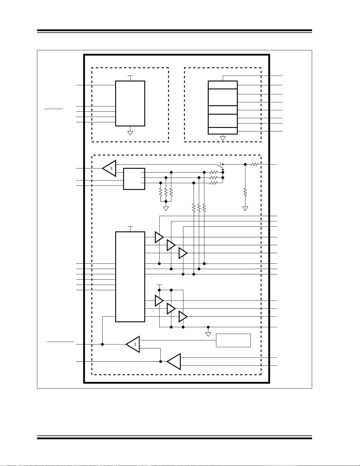
MOTOR CONTROL UNIT
COMMUNICATION PORT BIAS GENERATOR
+12V
HSA
HSB
HSC
LSA
LSB
LSC
VBA
VBB
VBC
GATE
CONTROL
LOGIC
I
I
I
I
I
I
I
I
I
O
O
O
O
O
O
O
VDD
I_OUT1
+
-
+
-
ILIMIT_OUT
I_SENSE1+
I_SENSE1-
DRIVER
FAULT
VDD
I
I
I/O
I/O
O
I
I
I
I
IO
PHASE DETECT
ILIMIT_REF
LDO
BUCK SMPS
SUPERVISOR
LDO
CHARGE PUMP
DE2
VDD
+5V
LX
FB
+12V
CAP2
CAP1
SIM Select
MCP8025/6
Functional Block Diagram – MCP8025
DS20005339A-page 4 2014 Microchip Technology Inc.
Page 5
GATE
CONTROL
LOGIC
CE
PWM1H
PWM1L
PWM2H
PWM2L
PWM3H
PWM3L
HV_IN1
I_OUT1
+
-
+
-
PHA
PHB
PHC
PGND
ILIMIT_OUT
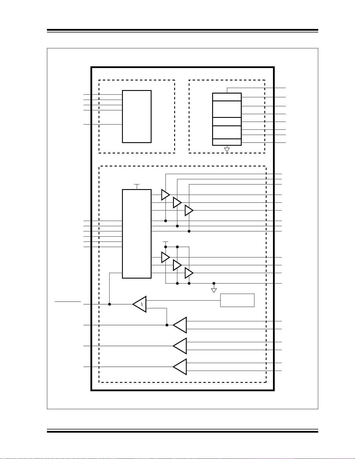
MOTOR CONTROL UNIT
COMMUNICATION PORT BIAS GENERATOR
+12V
HSA
HSB
HSC
I_SENSE1+
LSA
LSB
LSC
I_SENSE1-
VBA
VBB
VBC
LV_OUT1
LEVEL
TRANSLATOR
VDD
+
-
+
-
I_SENSE2+
I_SENSE2-
I_SENSE3+
I_SENSE3-
I_OUT2
I_OUT3
DRIVER
FAULT
I
I
I
I
I
I
I
I
I
I
I
O
O
O
O
O
O
O
O
LDO
BUCK SMPS
SUPERVISOR
LDO
CHARGE PUMP
DE2
VDD
+5V
LX
FB
+12V
CAP2
CAP1
ILIMIT_REF
HV_IN2
LV_OUT2
O
I
Functional Block Diagram – MCP8026
MCP8025/6
2014 Microchip Technology Inc. DS20005339A-page 5
Page 6
DS20005339A-page 6 2014 Microchip Technology Inc.
LIN
XCVR
CE
FAULTn/TXE
RX
TX
PWM1H
PWM1L
PWM2H
PWM2L
PWM3H
PWM3L
LIN_BUS
MUX
+
-
PHA
PHB
PHC
PGND
ZC_OUT
COMP_REF
NEUTRAL_SIM
DE2
MUX1
MUX2
MOTOR CONTROL UNIT
COMMUNICATION PORT BIAS GENERATOR
LDO
BUCK SMPS
SUPERVISOR
VDD
LDO
+5V
LX
FB
+12V
+12V
HSA
HSB
HSC
LSA
LSB
LSC
VBA
VBB
VBC
GATE
CONTROL
LOGIC
I
I
I
I
I
I
I
I
I
O
O
O
O
O
O
O
VDD
I_OUT1
+
-
+
-
ILIMIT_OUT
I_SENSE1+
I_SENSE1-
DRIVER
FAULT
VDD
I
I
I/O
I/O
O
I
I
I
I
IO
CAP1
CHARGE PUMP
CB
A
+
_
E
VADJ
PHASE DETECT
+12V
ILIMIT_REF
CAP2
100 nF
Ceramic
SIM Select
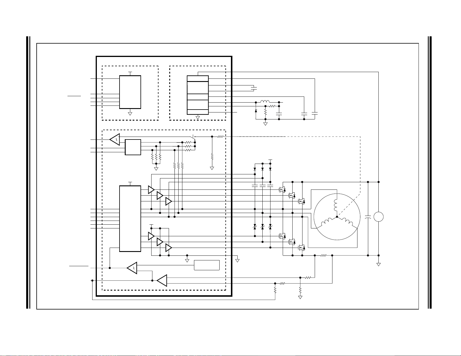
Typical Application Circuit – MCP8025
MCP8025/6
Page 7
2014 Microchip Technology Inc. DS20005339A-page 7
'!4%
#/.42/,
,/')#
#%
07-(
07-,
07-(
07-,
07-(
07-,
(6?).
)?/54
0(!
0("
0(#
0'.$
-/4/2#/.42/,5.)4
#/--5.)#!4)/.0/24
6
(3!
(3"
(3#
)?3%.3%
,3!
,3"
,3#
)?3%.3%
6"!
6""
6"#
,6?/54
,%6%,
42!.3,!4/2
6$$
)?3%.3%
)?3%.3%
)?3%.3%
)?3%.3%
)?/54
)?/54
$2)6%2
&!5,4
)
)
)
)
)
)
)
)
)
)
)
/
/
/
/
/
/
/
/
#"
!
?
%
6
$%
")!3'%.%2!4/2
,$/
"5#+3-03
350%26)3/2
6$$
,$/
6
,8
&"
6
#!0
#(!2'%05-0
6!$*
ILIMIT_REF
#!0
(6?).
,6?/54
/
)
N&
#ERAMIC
),)-)4?/54
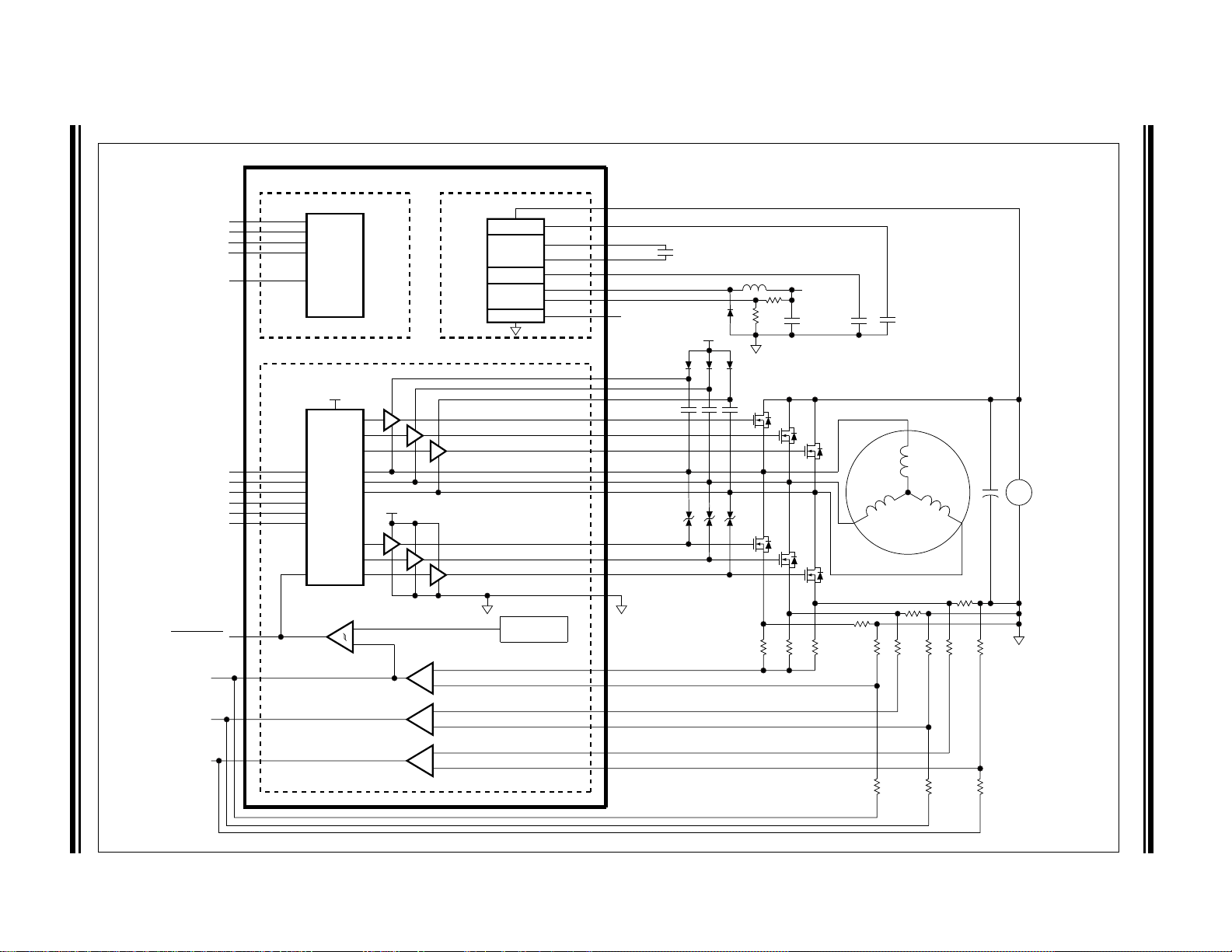
Typical Application Circuit – MCP8026
MCP8025/6
Page 8

MCP8025/6
NOTES:
DS20005339A-page 8 2014 Microchip Technology Inc.
Page 9
MCP8025/6
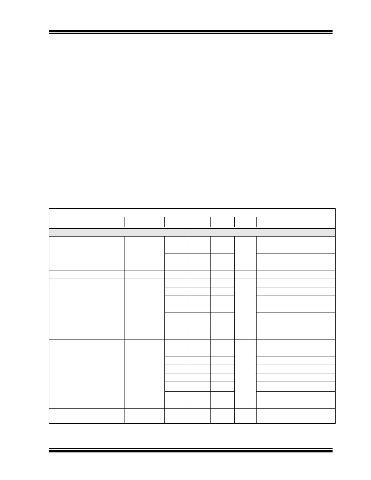
1.0 ELECTRICAL CHARACTERISTICS
† Notice: Stresses above those listed under “Maximum
Ratings” may cause permanent damage to the device.
This is a stress rating only and functional operation of
the device at those or any other conditions above those
Absolute Maximum Ratings †
Input Voltage, VDD.............................(GND – 0.3V) to +46.0V
Input Voltage, < 100 ms Transient ...............................+48.0V
Internal Power Dissipation ...........................Internally-Limited
Operating Ambient Temperature Range .......-40°C to +150°C
Operating Junction Temperature (Note 2) ....-40°C to +160°C
Transient Junction Temperature (Note 1)...................+170°C
Storage Temperature (Note 2)......................-55°C to +150°C
Digital I/O .......................................................... -0.3V to 5.5V
LV Analog I/O.................................................... -0.3V to 5.5V
VBx ..................................................(GND – 0.3V) to +46.0V
PHx, HSx .........................................(GND – 5.5V) to +46.0V
ESD and Latch-Up Protection:
, LIN_BUS/HV_IN1 8 kV HBM and 750V CDM
V
DD
All other pins ..................... 2 kV HBM and 750V CDM
Latch-up protection – all pins .............................. > 100 mA
indicated in the operational listings of this specification
is not implied. Exposure to maximum rating conditions
for extended periods may affect device reliability.
Note 1: Transient junction temperatures should not
2: The maximum allowable power dissipation
AC/DC CHARACTERISTICS
Electrical Specifications: Unless otherwise noted, T
Parameters Symbol Min. Typ. Max. Units Conditions
POWER SUPPLY INPUT
Input Operating Voltage V
Transient Maximum Voltage V
Input Current (MCP8025)V
Input Current (MCP8026)V
Digital Input/Output DIGITAL
Digital Open-Drain Drive
DD
DDmax
DD
DD
DIGITAL
I/O
IOL
Streng th
Note 1: 1000 hour cumulative maximum for ROM data retention (typical).
2: Limits are by design, not production tested.
= -40°C to +150°C, typical values are for +25°C, VDD=13V.
J
6.0 — 19.0 V Operating (MCP8025)
6.0 — 28.0 Operating (MCP8026)
6.0 — 40.0 Shutdown
4.0 — 32.0 Buck Operating Range
— — 48.0 V < 100 ms
———µAVDD>13V
— 5 15 Sleep Mode
— 175 — Standby, CE = 0V, T
— 175 — Standby, CE = 0V, TJ= +25°C
— 195 300 Standby, CE = 0V, T
—940— Active, CE>V
—1150— Active, VDD=6V, TJ=+25°C
———µAVDD>13V
— 5 15 Sleep Mode
— 120 — Standby, CE = 0V, T
— 120 — Standby, CE = 0V, TJ= +25°C
— 144 300 Standby, CE = 0V, T
—950— Active, CE>V
— 1090 — Active, VDD=6V, TJ=+25°C
0—5.5V
—1—mAVDS<50mV
exceed one second in duration. Sustained
junction temperatures above 170°C may
impact the device reliability.
is a function of ambient temperature, the
maximum allowable junction temperature
and the thermal resistance from junction to
air (i.e., T
, TJ, JA). Exceeding the maxi-
A
mum allowable power dissipation may
cause the device operating junction temperature to exceed the maximum 160°C
rating. Sustained junction temperatures
above 150°C can impact the device reliability and ROM data retention.
=-45°C
J
= +150°C
J
DIG_HI_TH
=-45°C
J
= +150°C
J
DIG_HI_TH
2014 Microchip Technology Inc. DS20005339A-page 9
Page 10
MCP8025/6
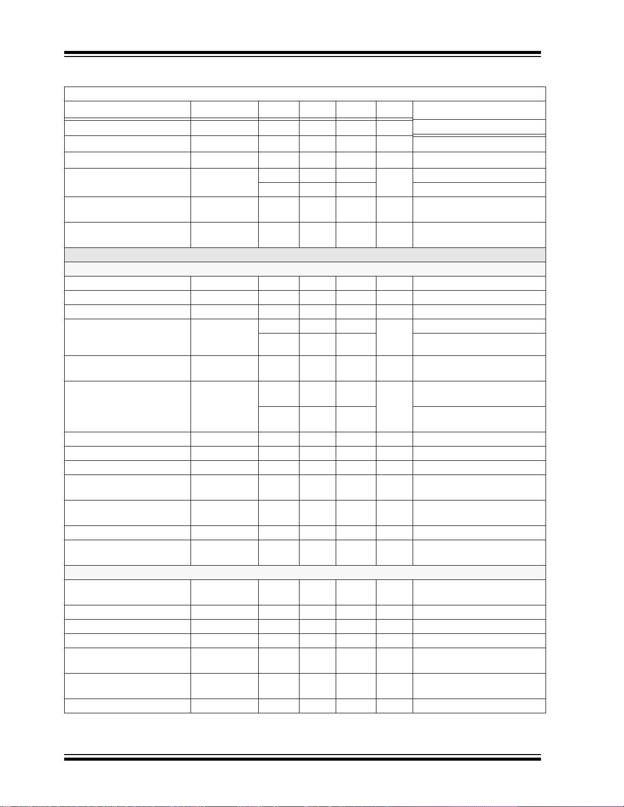
AC/DC CHARACTERISTICS (CONTINUED)
Electrical Specifications: Unless otherwise noted, T
Parameters Symbol Min. Typ. Max. Units Conditions
Digital Input Rising Threshold V
Digital Input Falling Threshold V
Digital Input Hysteresis V
Digital Input Current I
Analog Low-Voltage Input ANALOG
Analog Low-Voltage Output
DIG_HI_TH
DIG_LO_TH
DIG_HYS
DIG
ANALOG
VIN
VOUT
BIAS GENERATOR
+12V Regulated Charge Pump
Charge Pump Current I
Charge Pump Start CP
Charge Pump Stop CP
Charge Pump Frequency
CP
CP
START
STOP
FSW
(50% charging/
50% discharging)
Charge Pump Switch
CP
RDSON
Resistance
Output Voltage V
Output Voltage Tolerance |TOLV
Output Current I
Output Current Limit I
Output Voltage Temperature
TCV
OUT12
OUT12
OUT
LIMIT
OUT12
|— — 4.0 %I
Coefficient
Line Regulation |V
(V
OUT
Load Regulation |V
Power Supply Rejection
/
OUT
x VDD)|
OUT/VOUT
|— 0.2 0.5 %I
PSRR — 60 — dB f = 1 kHz, I
Ratio
+5V Linear Regulator
Output Voltage V
Output Voltage Tolerance |TOLV
Output Current I
Output Current Limit I
Output Voltage Temperature
|TCV
OUT5
|— — 4.0 %
OUT5
OUT
LIMIT
|—50—ppm/°C
OUT5
Coefficient
Line Regulation |V
(V
OUT
Load Regulation |V
/
OUT
x VDD)|
OUT/VOUT
|— 0.2 0.5 %I
Note 1: 1000 hour cumulative maximum for ROM data retention (typical).
2: Limits are by design, not production tested.
= -40°C to +150°C, typical values are for +25°C, VDD= 13V.
J
1.26 — — V
——0.54V
—500—mV
—30100µAV
—0.2— V
0 — 5.5 V Excludes LIN and high-voltage
0—V
OUT5
20 — — mA VDD=9.0V
11.0 11.5 — V VDD falling
— 12.0 12.5 V VDD rising
— 76.80 — kHz VDD=9.0V
—0— V
—14— RDSON sum of high side and
—12— VVDD 7.5V, C
—9— V
30 — — mA Average current
40 50 — mA Average current
—50—ppm/°C
—0.10.5%/V13V<V
—5—VVDD=V
30 — — mA Average current
40 50 — mA Average current
—0.10.5%/V6V<V
=3.0V
DIG
=0V
DIG
pins
V Excludes LIN and high-voltage
pins
= 13V (stopped)
DD
low side
=100nF,
DD
OUT5
DD
PUMP
PUMP
< 19V,
=10mA
OUT
+1V,
<19V, I
= 260 nF,
=20mA
OUT
=20mA
I
OUT
=5.1V, C
DD
=15mA
I
OUT
=1mA
OUT
=20mA
I
OUT
= 0.1 mA to 15 mA
OUT
=1mA
I
OUT
= 0.1 mA to 15 mA
OUT
DS20005339A-page 10 2014 Microchip Technology Inc.
Page 11
MCP8025/6
AC/DC CHARACTERISTICS (CONTINUED)
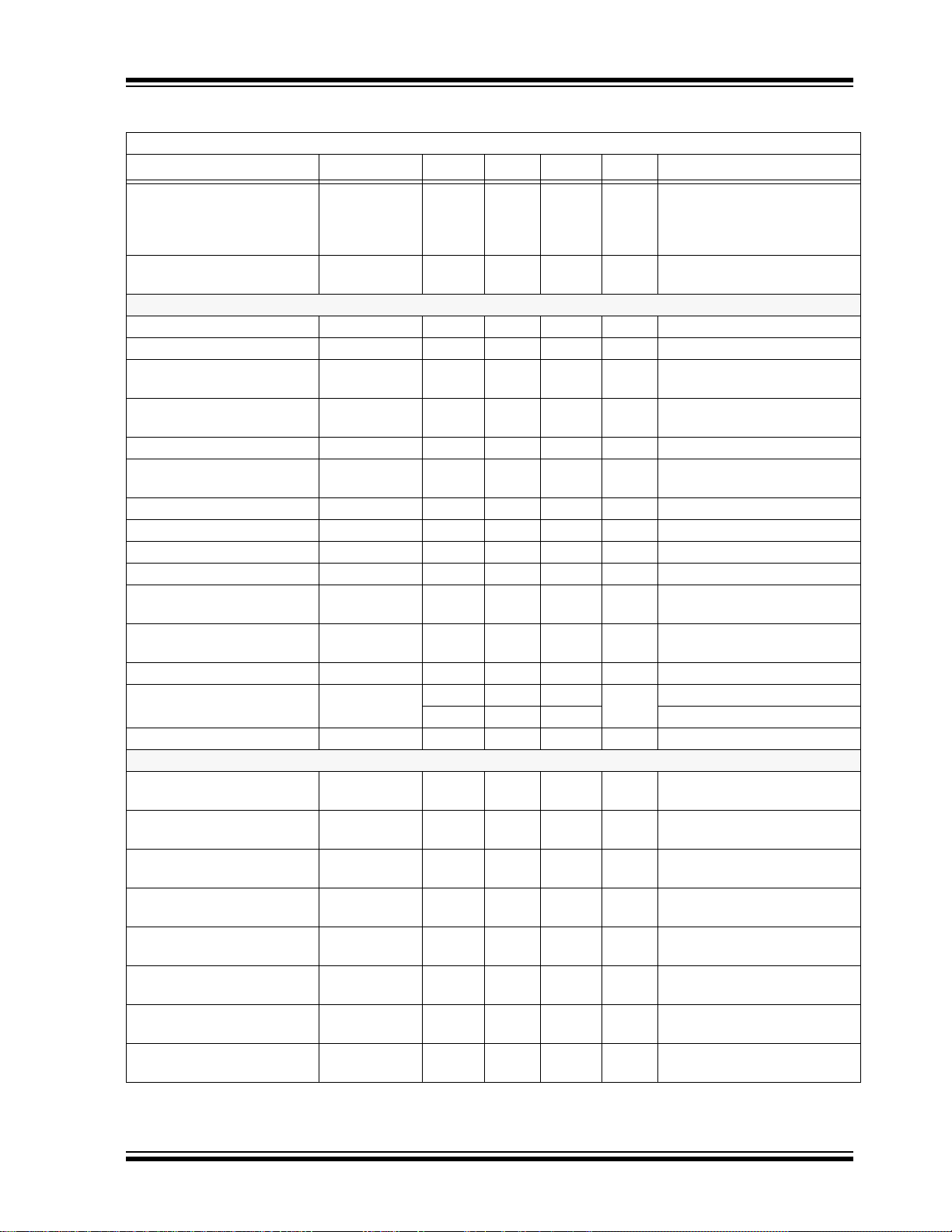
Electrical Specifications: Unless otherwise noted, T
Parameters Symbol Min. Typ. Max. Units Conditions
Dropout Voltage VDD–V
Power Supply Rejection
OUT5
PSRR — 60 — dB f = 1 kHz, I
Ratio
Buck Regulator
Feedback Voltage V
FB
Feedback Voltage Tolerance TOLVFB ——5.0%IFB=1µA
Feedback Voltage Line
Regulation
Feedback Voltage Load
V
V
V
)/
FB/VFB
|
DD
|—0.10.5%I
FB/VFB
Regulation
Feedback Input Bias Current I
Feedback Voltage
FB
V
BUCK_DIS
To Shutdown Buck Regulator
Switching Frequency f
Duty Cycle Range DC
PMOS Switch On Resistance R
PMOS Switch Current Limit I
Ground Current –
SW
MAX
DSON
P(MAX)
I
GND
PWM Mode
Quiescent Current –
I
Q
PFM Mode
Output Voltage Adjust Range V
Output Current I
Output Power P
OUT
OUT
OUT
V oltage Supervisor
Buck Input Undervoltage
UVLO
BK_STRT
Lockout – Start-Up
Buck Input Undervoltage
UVLO
BK_STOP
Lockout – Shutdown
Buck Input Undervoltage
UVLO
BK_HYS
Lockout Hysteresis
5V LDO Undervoltage Fault
UVLO
5VLDO_INACT
Inactive
5V LDO Undervoltage Fault
UVLO
5VLDO_ACT
Active
5V LDO Undervoltage Fault
UVLO
5VLDO_HYS
Hysteresis
Input Undervoltage Lockout –
UVLO
STRT
Start -Up
Input Undervoltage Lockout -
UVLO
STOP
Shutdown
Note 1: 1000 hour cumulative maximum for ROM data retention (typical).
2: Limits are by design, not production tested.
= -40°C to +150°C, typical values are for +25°C, VDD=13V.
J
—180350mVI
OUT
=20mA,
measurement taken when
output voltage drops 2% from
no-load value.
1.19 1.25 1.31 V
—0.10.5%/VV
= 6V to 28V
DD
= 5 mA to 150 mA
OUT
-100 — +100 nA Sink/Source
2.5 — 5.5 V VDD>6V
—461—kHz
3—96%
—0.6— TJ=25°C
—2.5— A
— 1.5 2.5 mA Switching
—150200µAI
OUT
=0mA
2.0 — 5.0 V
150 — — mA 5V, VDD–V
250 — — 3V, VDD–V
—750—mWP=I
OUTxVOUT
—4.34.5 VVDD rising
3.8 4.0 — V VDD falling
—0.3— V
—4.5— VV
—4.0— VV
OUT5
OUT5
rising
falling
—0.5— V
—6.06.25VVDD rising
5.1 5.5 — V VDD falling
OUT
OUT
OUT
=10mA
>0.5V
> 0.5V
2014 Microchip Technology Inc. DS20005339A-page 11
Page 12
MCP8025/6
AC/DC CHARACTERISTICS (CONTINUED)
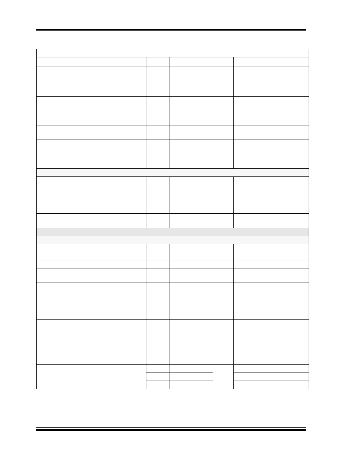
Electrical Specifications: Unless otherwise noted, T
Parameters Symbol Min. Typ. Max. Units Conditions
Input Undervoltage Lockout
UVLO
HYS
Hysteresis
Input Overvoltage Lockout –
DOVLO
STOP
Driver Disabled (MCP8025)
Input Overvoltage Lockout –
DOVLO
STRT
Driver Enabled (MCP8025)
Input Overvoltage Lockout
DOVLO
HYS
Hysteresis (MCP8025)
Input Overvoltage Lockout –
AOVLO
STOP
All Functions Disabled
Input Overvoltage Lockout –
AOVLO
STRT
All Functions Enabled
Input Overvoltage Lockout
AOVLO
HYS
Hysteresis
Temperature Supervisor
Thermal Warning
T
WARN
Temperature
Thermal Warning Hysteresis T
Thermal Shutdown
WARN
T
SD
Temperature
Thermal Shutdown
T
SD
Hysteresis
MOTOR CONTROL UNIT
Output Drivers
PWMH/L Input Pull Down R
Output Driver Source Current I
Output Driver Sink Current I
Output Driver Source
PULLDN
SOURCE
SINK
R
DSON
Resistance
Output Driver Sink
R
DSON
Resistance
Output Driver Blanking t
Output Driver UVLO
BLANK
D
UVLO
Threshold
Output Driver UVLO
t
DUVLO
Minimum Duration
Output Driver HS Drive
V
HS
Voltage
Output Driver LS Drive
V
LS
Voltage
Output Driver Bootstrap
V
BOOTSTRAP
Voltage
Note 1: 1000 hour cumulative maximum for ROM data retention (typical).
2: Limits are by design, not production tested.
= -40°C to +150°C, typical values are for +25°C, VDD= 13V.
J
0.20 0.45 0.70 V
— 20.0 20.5 V VDD rising
18.75 19.5 — V VDD falling
0.15 0.5 0.75 V
— 32.0 33.0 V VDD rising
29.0 30.0 — V VDD falling
1.0 2.0 3.0 V
—72—%TSDRising temperature (115°C)
— 15 — °C Falling temperature
160 170 — °C Rising temperature
— 25 — °C Falling temperature
—47—k
0.3 — — A VDD= 12V, HS[A:C], LS[A:C]
0.3 — — A VDD= 12V, HS[A:C], LS[A:C]
—17— I
—17— I
500 — 4000 ns Configurable
7.2 8.0 — V Config Register 0 bit 3 = 0
t
BLANK
+700
—t
BLANK
+1400
8.0 12 13.5 V With respect to the Phase pin
-5.5 — — With respect to ground
8.0 12 13.5 V With respect to ground
— — — V With respect to ground
— — 44 Continuous
— — 48 < 100 ms
=10mA, VDD= 12V,
OUT
HS[A:C], LS[A:C]
=10mA, VDD= 12V,
OUT
HS[A:C], LS[A:C]
ns Fault latched after t
DUVLO
DS20005339A-page 12 2014 Microchip Technology Inc.
Page 13

AC/DC CHARACTERISTICS (CONTINUED)
Electrical Specifications: Unless otherwise noted, T
Parameters Symbol Min. Typ. Max. Units Conditions
Output Driver Phase Pin
V
PHASE
Voltage
Output Driver Short Circuit
D
SC_THR
Protection Threshold
High Side (VDD–V
Low Side (V
PHx–PGND
Output Driver Short Circuit
PHx
)
)
T
SC_DLY
Detected Propagation Delay
Output Driver OVLO Turn-Off
T
OVLO_DLY
Delay
Power-Up or Sleep to
t
POWER
Standby
Standby to Motor Operational t
Fault to Driver Output
MOTOR
T
FAULT_ OFF
Turn-Off
CE Low to Driver Output
T
DEL_OFF
Turn-Off
CE Low to Standby State t
CE Low to Sleep State t
CE Fault Clearing Pulse t
STANDBY
SLEEP
FAULT_CLR
Current Sense Amplifier
Input Offset Voltage V
Input Offset Temperature Drift V
Input Bias Current I
Common Mode Input Range V
OS
CMR
OS
B
/T
A
Note 1: 1000 hour cumulative maximum for ROM data retention (typical).
2: Limits are by design, not production tested.
= -40°C to +150°C, typical values are for +25°C, VDD=13V.
J
— — — V With respect to ground
-5.5 — 44 Continuous
-5.5 — 48 < 100 ms
— — — V Set In Register CFG0
—0.250— 00 (Default)
—0.500— 01
—0.750— 10
—1.000— 11
———nsC
— 430 — Detection after blanking
— 10 — Detection during blanking,
3 5 — µs Detection synchronized with
— — — ms CE High-Low-High
—10— MCP8025
—5— MCP8026
— 5 — µs CE High-Low-High
— — 5 ms Standby state to Operational
— — 10 ms Standby state to Operational
———µsC
— 1 — UVLO, OCP faults
— 10 — All other faults
—100250nsC
— 1 — ms Time after CE = Low,
— 1 — ms Time after CE = Low,
1 — 900 µs CE High-Low-High Transition
-3.0 — +3.0 mV VCM=0V
—±2.0—µV/°CVCM=0V
-1 — +1 µA
-0.3 — 3.5 V
MCP8025/6
= 1000 pF, VDD=12V
LOAD
value is delay after blanking
internal clock (Note 2)
Transition < 100 µs (Fault
Clearing)
Transition < 0.9 ms (Fault
Clearing)
state (MCP8025, Note 2)
state (MCP8026, Note 2)
= 1000 pF, VDD=12V,
LOAD
time after fault occurs.
= 1000 pF, VDD=12V,
LOAD
Time after CE = Low (Note 2)
SLEEP Bit = 0
SLEEP Bit = 1
Time (Note 2)
= -40°C to +150°C
T
A
2014 Microchip Technology Inc. DS20005339A-page 13
Page 14
MCP8025/6
AC/DC CHARACTERISTICS (CONTINUED)
Electrical Specifications: Unless otherwise noted, T
Parameters Symbol Min. Typ. Max. Units Conditions
Common Mode Rejection
CMRR — 80 — dB Freq = 1 kHz, I
Ratio
Maximum Output Voltage
, V
V
OL
OH
Swing
Slew Rate SR — ±7 — V/µs Symmetrical
Gain Bandwidth Product GBWP — 10.0 — MHz
Current Comparator
CC
HYS
Hysteresis
Current Comparator
V
CC_CMR
Common Mode Input Range
Current Limit DAC
Resolution — 8 — Bits
Output Voltage Range V
Output Voltage V
Input to Output Delay T
, V
OL
DAC
DELAY
OH
Integral Nonlinearity INL -0.5 — +0.5 %FSR %Full Scale Range, Note 2
Differential Nonlinearity DNL -50 — +50 %LSB %LSB, Note 2
ILIMIT_OUT
Sink Current
IL
OUT
(Open-Drain)
ZC Back EMF Sampler Comparator (MCP8025)
Maximum Output Voltage
Swing
Reference Input Impedance ZC
Input to Output Delay ZC
Voltage Divider RC Time
ZCVOL,
ZCV
OH
ZREF
DELAY
ZC
TRC
Constant
ZC Output Pull-Up Range ZC
ZC Output Sink Current
RPULLUP
ZC
IOL
(Open-Drain)
Back EMF Sampler Phase Multiplexer (MCP8025)
MUX[1:2] Input Pull Down R
Transition Time t
Delay from MUX Select to ZC
PULLDN
MUX
TRAN
DELAY
Out
Phase Filter Capacitors C
PHASE
COMMUNICATION PORTS
Standard LIN (MCP8025)
Microcontroller Interface
TX Input Pull-Up Resistor R
PUTXD
Note 1: 1000 hour cumulative maximum for ROM data retention (typical).
2: Limits are by design, not production tested.
= -40°C to +150°C, typical values are for +25°C, VDD= 13V.
J
OUT
0.05 — 4.5 V I
OUT
= 200 µA
—10—mV
1.0 — 4.5 V
0.991 — 4.503 V I
OUT
=1mA
——— VCFG1 Code x
13.77 mV/bit + 0.991V
— 0.991 — Code 00H
— 1.872 — Code 40H
— 4.503 — Code FFH
—50—µs
—1—mAV
0.05 - 5.0 V I
ILIMIT_OUT
OUT
50 mV
=1mA
—83—k
—-500nsV
IN_STEP
=500mV, Note 2
—100— ns
3.3 10 — k
—1—mAVout 50 mV
—47—k
—150250nsNote 2
—210— ns
— 1.5 — pF MUX input to ground
—48 - k Pull up to 5V
=10µA
DS20005339A-page 14 2014 Microchip Technology Inc.
Page 15
AC/DC CHARACTERISTICS (CONTINUED)
Electrical Specifications: Unless otherwise noted, T
Parameters Symbol Min. Typ. Max. Units Conditions
Bus Interface
LIN Bus High-Level Input
V
HI
Voltage
LIN Bus Low-Level Input
V
LO
Voltage
LIN Bus Input Hysteresis V
LIN Bus Low-Level Output
HYS
I
OL
Current
LIN Bus Input Pull-Up Current I
LIN Bus Short Circuit Current
Limit
LIN Bus Low-Level Output
PU
I
SC
V
OL
Voltage
LIN Bus Input Leakage
Current (at receiver during
I
BUS_PAS_DOM
dominant bus level)
LIN Bus Input Leakage
Current (at receiver during
recessive bus level)
I
BUS_PAS_REC
LIN Bus Input Leakage
Current (disconnected from
I
BUS_NO_GND
ground)
LIN Bus Input Leakage
I
BUS_NO_BAT
Current (disconnected from
V
)
DD
Receiver Center Voltage V
LIN Bus Slave Pull-Up
BUS_CNT
R
PULLUP
Resistance
LIN Dominant State Timeout t
Propagation Delay T
Symmetry T
DOM_TOUT
RX_PD
RX_SYM
V oltage Level Translators (MCP8026)
High Voltage Input Range V
Low Voltage Output Range V
IN
OUT
Input Pull-Up Resistor RPU — 30 — k
High-Level Input Voltage V
Low-Level Input Voltage V
Input Hysteresis V
Propagation Delay T
IH
IL
HYS
LV_ OUT
Note 1: 1000 hour cumulative maximum for ROM data retention (typical).
2: Limits are by design, not production tested.
= -40°C to +150°C, typical values are for +25°C, VDD=13V.
J
0.6 x
V
DD
— — V Recessive state
——0.4x
V
DD
— — 0.175 x
V
DD
7.3 — — mA VO=0.2xVDD, VDD=8V
16.5 — — VO=0.2xVDD, VDD= 18V
30.6 — — V
5—180µA
50 — 200 mA
——0.2x
V
DD
-1 — — mA Driver OFF,
— 12 20 µA Driver OFF,
-1 — 1 mA GND = VDD=12V,
——10µAVDD=0V,
0.475 x
V
DD
0.5 x
V
DD
0.525 x
V
DD
20K 30K 47K
—25—ms
— 3.0 6.0 µs Propagation delay of receiver
-2 — +2 µs Symmetry of receiver
0—VDDV
0—5.0VV
0.60 — — V
——0.40VDDVDD=15V
——0.30V
—3.06.0µsNote 2
MCP8025/6
VDominant state
VVHI–V
V
VV
DDVDD
DD
LO
=0.251xVDD, VDD= 18V
O
=0V, VDD=12V
V
BUS
V
V
BUS
7V < V
7V < V
0V < V
0V < V
BUS _CNT
DD
< 19V
BUS
<19V
DD
< 19V
BUS
< 19V
BUS
=(VHI–VLO)/2
propagation delay rising edge
w.r.t.falling edge
=15V
2014 Microchip Technology Inc. DS20005339A-page 15
Page 16
MCP8025/6
AC/DC CHARACTERISTICS (CONTINUED)
Electrical Specifications: Unless otherwise noted, T
Parameters Symbol Min. Typ. Max. Units Conditions
Maximum Communication
F
MAX
Frequency
Low-Voltage Output Sink
I
OL
Current (Open-Drain)
DE2 Communications
Baud Rate BAUD — 9600 — BPS
Power-Up Delay PU_DELAY — 1 — ms Time from rising V
DE2 Sink Current DE2
DE2 Message Response
DE2
iSINK
RSP
Time
DE2 Host Wait Time DE2
DE2 Message Receive
DE2
WAIT
RCVTOUT
Timeout
INTERNAL ROM (READ-ONLY MEMORY) DATA RETENTION
Cell High Temperature
HTOL — 1000 — Hours T
Operating Life
Cell Operating Life — 10 — Years T
Note 1: 1000 hour cumulative maximum for ROM data retention (typical).
2: Limits are by design, not production tested.
= -40°C to +150°C, typical values are for +25°C, VDD= 13V.
J
——20kHzNote 2
—1—mAV
OUT
50 mV
to DE2 active
1——mAV
50 mV, Note 2
DE2
0 µs Time from last received Stop bit
to Response Start bit, Note 2
3.125 — — ms Minimum Time For Host
To Wait For Response. Three
packets based on 9600 BAUD,
Note 2
— 5 — ms Time between message bytes
= 150°C (Note 1)
J
= 85°C
J
DD
6V
TEMPERATURE SPECIFICATIONS
Parameters Sym. Min. Typ. Max. Units Conditions
Temperature Ranges (Note 1)
Specified Temperature Range T
Operating Temperature Range T
Storage Temperature Range T
A
A
T
J
A
Package Thermal ResistanceS
Thermal Resistance, 5 mm x 5 mm
40L-QFN
Thermal Resistance, 7 mm x 7 mm
48L-TQFP with Exposed Pad
JA
JC
JA
JC
Note 1: The maximum allowable power dissipation is a function of ambient temperature, the maximum allowable
junction temperature and the thermal resistance from junction to air (i.e., T
maximum allowable power dissipation will cause the device operating junction temperature to exceed the
maximum 160°C rating. Sustained junction temperatures above 160°C can impact the device reliability.
2: 1000 hour cumulative maximum for ROM data retention (typical).
-40 +150 °C
-40 +150 °C
-40 +160 °C
-55 +150 °C (Note 2)
— 37 — °C/W 4-Layer JC51-5 standard board,
—6.9—
natural convection
—30—°C/W
—15—
, TJ, JA). Exceeding the
A
DS20005339A-page 16 2014 Microchip Technology Inc.
Page 17

MCP8025/6
ESD, SUSCEPTIBILITY, SURGE AND LATCH-UP TESTING
Parameter Standard and Test Condition Value
Input voltage surges ISO 16750-2 28V for 1 minute,
45V for 0.5 seconds
ESD according to IBEE LIN EMC
– Pins LIN_BUS, V
ESD HBM with 1.5 k/100 pF CEI/IEC 60749-26: 2006
ESD HBM with 1.5 k/100 pF
– Pins LIN_BUS, V
P
GND
ESD CDM (Charged Device Model,
field-induced method – replaces
machine-model method)
Latch-Up Susceptibility AEC Q100-004, 150°C > 100 mA
(HMM)
DD
, HV_IN1 against
DD
Test specification 1.0 following IEC
61000-4.2
AEC-Q100-002-Ref E
JEDEC JS-001-2012
CEI/IEC 60749-26: 2006
AEC-Q100-002-Ref E
JEDEC JS-001-2012
ESD-STM5.3.1-1999 ± 750V all pins
±8kV
±2kV
±8kV
2014 Microchip Technology Inc. DS20005339A-page 17
Page 18

MCP8025/6
NOTES:
DS20005339A-page 18 2014 Microchip Technology Inc.
Page 19

MCP8025/6
-0.010
-0.008
-0.006
-0.004
-0.002
0.000
0.002
0.004
0.006
0.008
0.010
-45 -20 5 30 55 80 105 130
155
V
OUT
= 5V
V
OUT
= 12V
0.00
0.05
0.10
0.15
0.20
0.25
0.30
0.35
-45 -20 5 30 55 80 105 130
155
Load Regulation (%)
V
OUT
= 5V
V
OUT
= 12V
012345678910
iLIMIT_OUT
DE2
0 5 10 15 20 25 30 35 40 45 50
HSA
V
BA
20
15
10
5
0
25
20
15
10
5
0
VDD= 6V
100
105
110
115
120
125
130
135
140
145
150
7 1013161922252831
Current (mA)
5V LDO
12V LDO
-40
-20
0
20
40
60
80
100
120
140
0
3
6
9
12
15
18
0 20406080100
V
IN
(V)
VIN= 14V
VIN= 15V
V
OUT
(AC)
CIN= C
OUT
= 10 µF
I
OUT
= 20 mA
2.0 TYPICAL PERFORMANCE CURVES
Note: The graphs and tables provided following this note are a statistical summary based on a limited number of
samples and are provided for informational purposes only. The performance characteristics listed herein
are not tested or guaranteed. In some graphs or tables, the data presented may be outside the specified
operating range (e.g., outside specified power supply range) and therefore outside the warranted range.
Note: Unless otherwise indicated, T
= +25°C; Junction Temperature (TJ) is approximated by soaking the device under
A
test to an ambient temperature equal to the desired junction temperature. The test time is small enough such that the
rise in Junction temperature over the Ambient temperature is not significant.
Volts (V)
Line Regulation (%/V)
Temperature (°C)
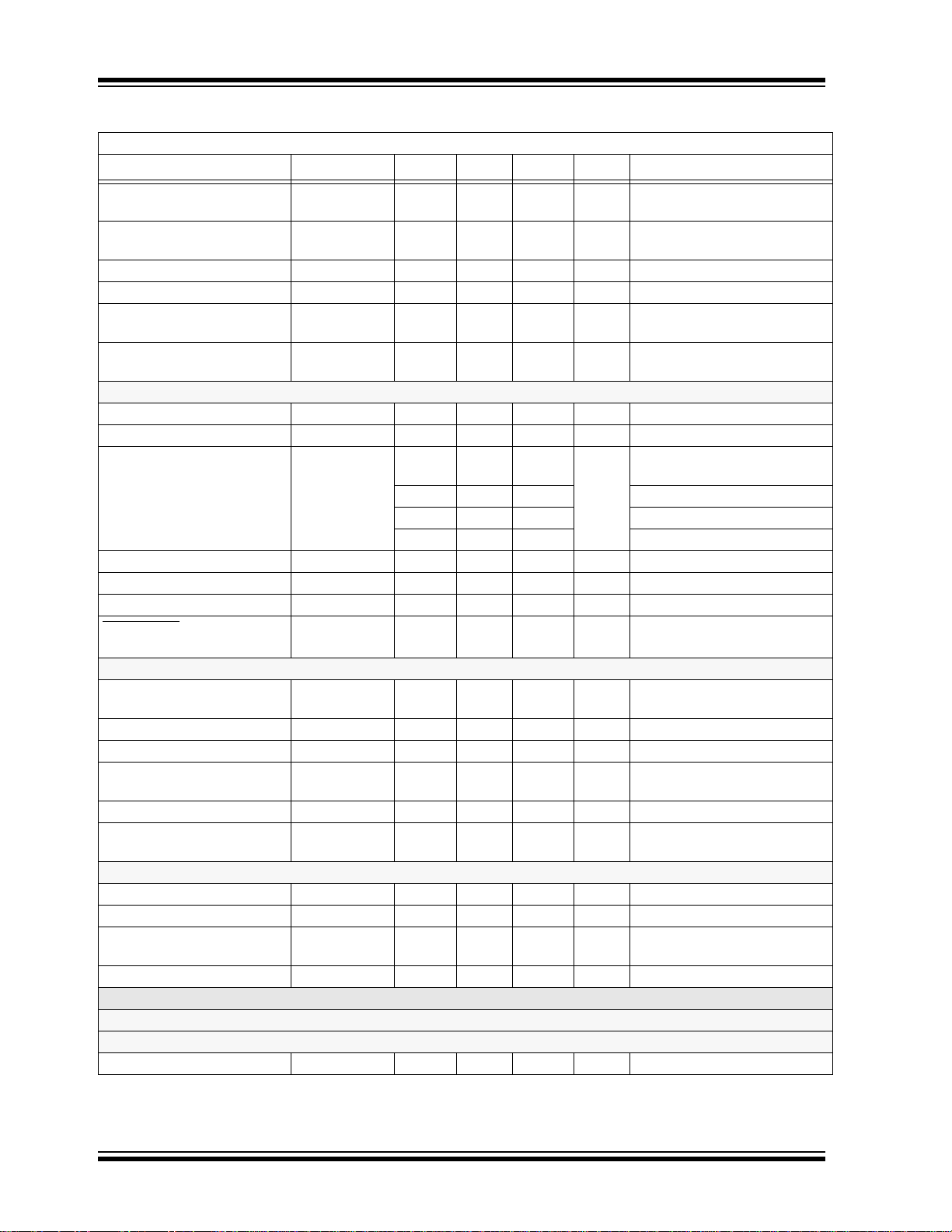
FIGURE 2-1: LDO Line Regulation vs. Temperature.
FIGURE 2-4: Bootstrap Voltage @ 92% Duty Cycle.
Time (µs)
Temperature (°C)
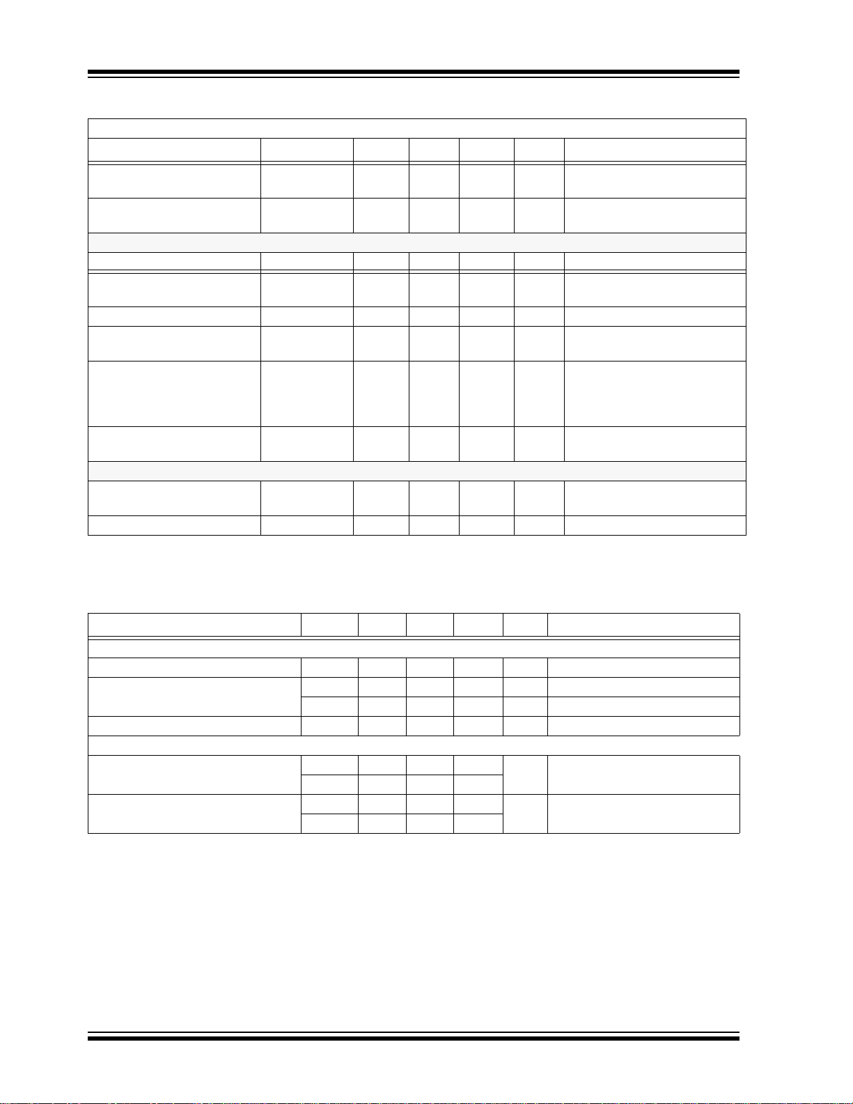
FIGURE 2-2: LDO Load Regulation vs. Temperature.
FIGURE 2-3: I
Message Delay.
2014 Microchip Technology Inc. DS20005339A-page 19
Time (µs)
LIMIT_OUT
Low to DE2
Voltage (V)
FIGURE 2-5: LDO Short Cir cuit Cur rent vs. Input Voltage.
(mV)
OUT
V
Time (µs)
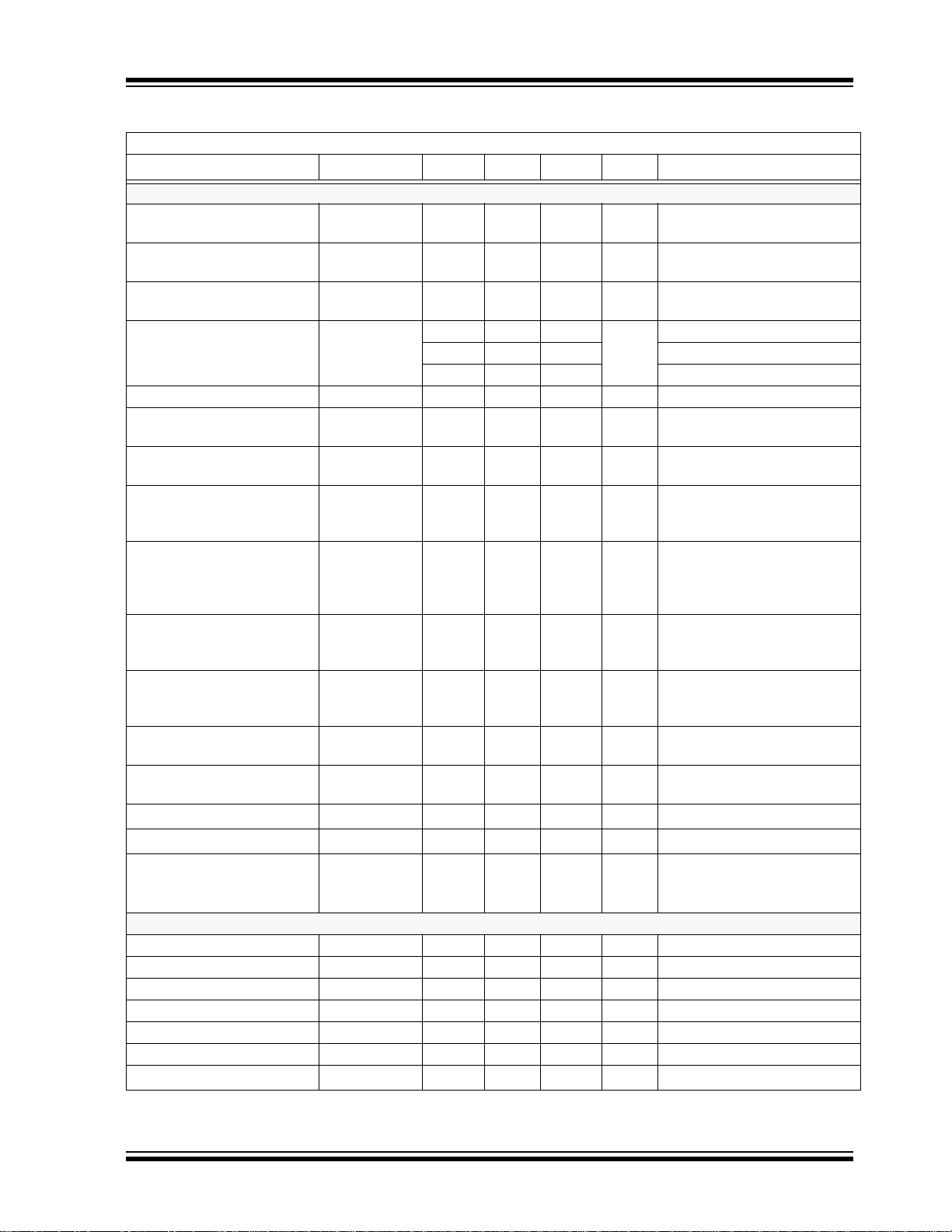
FIGURE 2-6: 5V LDO Dynamic Linestep –
Rising V
DD
.
Page 20
MCP8025/6
-40
-20
0
20
40
60
80
100
120
140
0
3
6
9
12
15
18
0 20406080100
V
IN
(V)
VIN= 15V
VIN= 14V
V
OUT
(AC)
CIN= C
OUT
= 10 µF
I
OUT
= 20 mA
-40
-20
0
20
40
60
80
100
120
140
0
3
6
9
12
15
18
0 20406080100
IN
VIN= 14V
VIN= 15V
V
OUT
(AC)
CIN= C
OUT
= 10 µF
I
OUT
= 20 mA
-40
-20
0
20
40
60
80
10
11
12
13
14
15
16
0 20406080100
IN
VIN= 15V
VIN= 14V
V
OUT
(AC)
CIN= C
OUT
= 10 µF
I
OUT
= 20 mA
-100
-80
-60
-40
-20
0
20
40
60
80
100
0.0 0.5 1.0 1.5 2.0 2.5
OUT
VIN= 14V
V
OUT
= 5V
C
IN
= C
OUT
= 10 µF
I
OUT
= 1 mA to 20 mA Pulse
20 mA
1 mA
-100
-80
-60
-40
-20
0
20
40
60
80
100
0.0 0.5 1.0 1.5 2.0 2.5
V
OUT
AC (mV)
1 mA
VIN= 14V
V
OUT
= 12V
C
IN
= C
OUT
= 10 µF
I
OUT
= 1 mA to 20 mA Pulse
20 mA
7.0
8.0
9.0
10.0
11.0
12.0
13.0
14.0
6 101418222630
V
OUT
(V)
V
OUT
= 12V
C
IN
= C
OUT
= 10 µF
I
OUT
= 20 mA
Charge Pump
Switch Point
Note: Unless otherwise indicated, T
= +25°C; Junction Temperature (TJ) is approximated by soaking the device under
A
test to an ambient temperature equal to the desired junction temperature. The test time is small enough such that the
rise in Junction temperature over the Ambient temperature is not significant.
(mV)
OUT
V
Time (µs)
FIGURE 2-7: 5V LDO Dynamic Linestep –
Falling V
(V)
V
DD
.
(mV)
OUT
V
AC (mV)
V
Time (ms)
FIGURE 2-10: 5V LDO Dynamic Loadstep.
Time (µs)
FIGURE 2-8: 12V LDO Dynamic Linestep
– Rising V
(V)
V
DD
.
Time (µs)
FIGURE 2-9: 12V LDO Dynamic Linestep
– Falling V
DS20005339A-page 20 2014 Microchip Technology Inc.
.
DD
(mV)
OUT
V
Time (ms)
FIGURE 2-11: 12V LDO Dynamic Loadstep.
VIN(V)
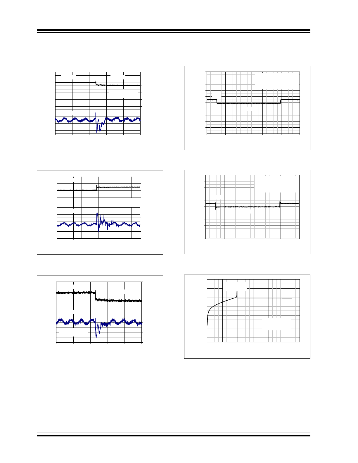
FIGURE 2-12: 12V LDO Output Voltage vs. Rising Input Voltage.
Page 21

MCP8025/6
0
200
400
600
800
1000
-45 -20 5 30 55 80 105 130 155
CE Low
CE High
0
200
400
600
800
1000
1200
-45 -20 5 30 55 80 105 130 155
CE Low
CE High
0.0 0.5 1.0 1.5 2.0 2.5 3.0 3.5 4.0 4.5 5.0
Dead Time
PWMxH
PWMxL
Dead Time
10
12
14
16
18
20
22
24
-45 -20 5 30 55 80 105 130 155
R
DSON
(
Ω
)
Low-Side
Note: Unless otherwise indicated, T
= +25°C; Junction Temperature (TJ) is approximated by soaking the device under
A
test to an ambient temperature equal to the desired junction temperature. The test time is small enough such that the
rise in Junction temperature over the Ambient temperature is not significant.
1200
High-Side
Quiescent Current (µA)
Temperature (°C)
FIGURE 2-13: Quiescent Current vs. Temperature (MCP8025).
FIGURE 2-16: Driver R
Temperature.
Temperature(°C)
DSON
vs.
Quiescent Current (µA)
Temperature (°C)
FIGURE 2-14: Quiescent Current vs. Temperature (MCP8026).
Time (µs)
FIGURE 2-15: 500 ns PWM Dead Time Injection.
2014 Microchip Technology Inc. DS20005339A-page 21
Page 22

MCP8025/6
NOTES:
DS20005339A-page 22 2014 Microchip Technology Inc.
Page 23

MCP8025/6
3.0 PIN DESCRIPTIONS
The descriptions of the pins are listed in Tables 3-1 and 3-2.
T ABLE 3-1: MCP8025 – PIN FUNCTION TABLE
QFN TQFP Symbol I/O Description
2 1 PWM1L I Digital input, phase A low-side control, 47 k pull down
3 2 PWM1H I Digital input, phase A high-side control, 47 k pull down
4 3 CE I Digital input, device enable, 47 k pull down
— 4 NC — No connection
— 5 NC — No connection
5 6 LIN_BUS I/O LIN Bus physical layer
—7 P
6 8 RX O LIN Bus receive data, open-drain
7 9 TX I LIN Bus transmit data
810FAULTn
9 11 MUX1 I Digital input Back EMF sampler phase multiplexer control, 47 k pull down
10 12 MUX2 I Digital input Back EMF sampler phase multiplexer control, 47 k pull down
11 13 ZC_OUT O Back EMF sampler comparator output, open-drain
12 14 COMP_REF I Back EMF sampler comparator reference
13 15 ILIMIT_OUT
14 16 I_OUT1 O Motor current sense amplifier output
15 17 ISENSE1- I Motor current sense amplifier inverting input
16 18 ISENSE1+ I Motor current sense amplifier non-inverting input
17 19,20 P
18 21 LSA O Phase A low-side N-channel MOSFET driver, active high
19 22 LSB O Phase B low-side N-channel MOSFET driver, active high
20 23 LSC O Phase C low-side N-channel MOSFET driver, active high
—24 P
21 25 HSC O Phase C high-side N-channel MOSFET driver, active high
22 26 HSB O Phase B high-side N-channel MOSFET driver, active high
23 27 HSA O Phase A high-side N-channel MOSFET driver, active high
24 28 PHC I/O Phase C high-side MOSFET driver reference, Back EMF sense input
25 29 PHB I/O Phase B high-side MOSFET driver reference, Back EMF sense input
26 30 PHA I/O Phase A high-side MOSFET driver reference, Back EMF sense input
27 31 V
28 32 V
29 33 V
30 34 +12V Power Analog circuitry and low-side gate drive bias
— 35, 36 P
31 37 LX Power Buck regulator switch node, external inductor connection
32 38, 39 V
33 40 FB I Buck regulator feedback node
34 41 +5V Power Internal circuitry bias
35 42 CAP2 Power Charge pump flying capacitor input
36 43 CAP1 Power Charge pump flying capacitor input
37 44 DE2 O Voltage and temperature supervisor output, open-drain
38 45 PWM3L I Digital input, phase C low-side control, 47 k pull down
39 46 PWM3H I Digital input, phase C high-side control, 47 k pull down
40 47 PWM2L I Digital input, phase B low-side control, 47 k pull down
1 48 PWM2H I Digital input, phase B high-side control, 47 k pull down
EP EP P
GND
/TXE I/O LIN transceiver fault and transmit enable
GND
GND
BC
BB
BA
GND
DD
GND
Power Power 0V reference
O Current limit comparator, MOSFET driver fault output, open-drain
Power Power 0V reference
Power Power 0V reference
Power Phase C high-side MOSFET driver bias
Power Phase B high-side MOSFET driver bias
Power Phase A high-side MOSFET driver bias
Power Power 0V reference
Power Input Supply
Power Exposed Pad. Connect to Power 0V reference.
2014 Microchip Technology Inc. DS20005339A-page 23
Page 24

MCP8025/6
TABLE 3-2: MCP8026 – PIN FUNCTION TABLE
QFN TQFP Symbol I/O Description
2 1 PWM1L I Digital input, phase A low-side control, 47 k pull down
3 2 PWM1H I Digital input, phase A high-side control, 47 k pull down
4 3 CE I Digital input, device enable, 47 k pull down
— 4 LV_OUT2 O Level Translator 2 logic level translated output, open-drain
— 5 HV_IN2 I Level Translator 2 high-voltage input, 30 k configurable pull up
5 6 HV_IN1 I Level Translator 1 high-voltage input, 30 k configurable pull up
—7 P
6 8 LV_OUT1 O Level Translator 1 logic level translated output, open-drain
7 9 I_OUT3 O Motor phase current sense amplifier 3 output
8 10 ISENSE3- I Motor phase current sense amplifier 3 inverting input
9 11 ISENSE3+ I Motor phase current sense amplifier 3 non-inverting input
10 12 I_OUT2 O Motor phase current sense amplifier 2 output
11 13 ISENSE2- I Motor phase current sense amplifier 2 inverting input
12 14 ISENSE2+ I Motor phase current sense amplifier 2 non-inverting input
13 15 ILIMIT_OUT
14 16 I_OUT1 O Motor current sense amplifier 1 output
15 17 ISENSE1- I Motor current sense amplifier 1 inverting input
16 18 ISENSE1+ I Motor current sense amplifier 1 non-inverting input
17 19,20 P
18 21 LSA O Phase A low-side N-Channel MOSFET driver, active high
19 22 LSB O Phase B low-side N-Channel MOSFET driver, active high
20 23 LSC O Phase C low-side N-Channel MOSFET driver, active high
—24 P
21 25 HSC O Phase C high-side N-Channel MOSFET driver, active high
22 26 HSB O Phase B high-side N-Channel MOSFET driver, active high
23 27 HSA O Phase A high-side N-Channel MOSFET driver, active high
24 28 PHC I/O Phase C high-side MOSFET driver reference, back EMF sense input
25 29 PHB I/O Phase B high-side MOSFET driver reference, back EMF sense input
26 30 PHA I/O Phase A high-side MOSFET driver reference, back EMF sense input
27 31 V
28 32 V
29 33 V
30 34 +12V Power Analog circuitry and low-side gate drive bias
— 35,36 P
31 37 LX Power Buck regulator switch node, external inductor connection
32 38, 39 V
33 40 FB I Buck regulator feedback node
34 41 +5V Power Internal circuitry bias
35 42 CAP2 Power Charge pump flying capacitor input
36 43 CAP1 Power Charge pump flying capacitor input
37 44 DE2 O Voltage and temperature supervisor output, open-drain
38 45 PWM3L I Digital input, phase C low-side control, 47 k pull down
39 46 PWM3H I Digital input, phase C high-side control, 47 k pull down
40 47 PWM2L I Digital input, phase B low-side control, 47 k pull down
1 48 PWM2H I Digital input, phase B high-side control, 47 k pull down
EP EP P
GND
GND
GND
BC
BB
BA
GND
DD
GND
Power Power 0V reference
O Current limit comparator, MOSFET driver fault output, open-drain
Power Power 0V reference
Power Power 0V reference
Power Phase C high-side MOSFET driver bias
Power Phase B high-side MOSFET driver bias
Power Phase A high-side MOSFET driver bias
Power Power 0V reference
Power Input supply
Power Exposed Pad. Connect to Power 0V reference.
DS20005339A-page 24 2014 Microchip Technology Inc.
Page 25

MCP8025/6
3.1 Low-Side PWM Inputs (PWM1L, PWM2L, PWM3L)
Digital PWM inputs for low-side driver control. Each
input has a 47 k pull down to ground. The PWM
signals may contain dead-time timing or the system
may use configuration register 2 to set the dead time.
3.2 High-Side PWM Inputs (PWM1H, PWM2H, PWM3H)
Digital PWM inputs for high-side driver control. Each
input has a 47 k pull down to ground. The PWM
signals may contain dead-time timing or the system
may use the configuration register 2 to set the dead
time.
3.3 No Connect (NC)
Reserved. Do not connect.
3.4 Chip Enable Input (CE)
Chip Enable input used to enable/disable the output
driver and on-board functions. When CE is high, all
device functions are enabled. When CE is low, the
device operates in Standby or Sleep mode. When
Standby mode is active, the current amplifiers and the
12V LDO are disabled. The buck regulator, the DE2
pin, the voltage and temperature sensor functions are
not affected. The 5V LDO is disabled on the MCP8026
The H-bridge driver outputs are all set to a low state
within 100 ns of CE = 0. The device transitions to
Standby or Sleep mode 1 ms after CE = 0.
The CE pin may be used to clear any hardware faults.
When a fault occurs, the CE input may be used to clear
the fault by setting the pin low and then high again. The
fault is cleared by the rising edge of the CE signal if the
hardware fault is no longer active.
The CE pin is used to enable Sleep mode when the
SLEEP bit in the CFG0 configuration register is set to 1.
CE must be low for a minimum of 1 ms before the
transition to Standby or Sleep mode occurs. This allows
time for CE to be toggled to clear any faults without
going into Sleep mode.
The CE pin is used to awaken the device from the
Sleep mode state. To awaken the device from a Sleep
mode state, the CE pin must be set low for a minimum
of 250 μs. The device will then wake up with the next
rising edge of the CE pin.
The CE pin has an internal 47 k pull down.
3.5 Level Translators (HV_IN1, HV_IN2, LV_OUT1, LV_OUT2)
Unidirectional digital level translators. These pins
translate digital input signal on the HV_INx pin to a
low-level digital output signal on the LV_OUTx pin. The
HV_INx pins have internal 30 k pull ups to V
are controlled by bit PU30K in the CFG0 configuration
register. The PU30K bit is only sampled during CE = 0.
The HV_IN1 pin has higher ESD protection than the
HV_IN2 pin. The higher ESD protection makes the
HV_IN1 pin better suited for connection to external
switches.
LV_OUT1 and LV_OUT2 are open-drain outputs. An
external pull-up resistor to the low-voltage logic supply
is required.
The HV_IN1 pin may be used to awaken the device
from the Sleep mode state. The MCP8026 will awaken
on the rising edge of the pin after detecting a low state
lasting > 250 µs on the pin.
DD
that
3.6 LIN Transceiver Bus (LIN_BUS)
The bidirectional LIN_BUS interface pin connects to
the LIN Bus network. The LIN_BUS driver is controlled
by the TX pin. The driver is an open-drain output. The
MCP8025 device contains a LIN Bus 30 k pull-up
resistor that may be enabled or disabled by setting the
PU30K bit in the CFG0 configuration register. The pull
up may only be changed while in Standby mode.
During normal operation, the 30 k pull up is always
enabled. In Sleep mode, the 30 k pull up is always
disabled.
The LIN bus may be used to awaken the device from
the Sleep mode state. When a LIN wake-up event is
detected on the LIN_BUS pin, the device will wake up.
The MCP8025 will awaken on the rising edge of the
bus after detecting a dominant state lasting > 150 µs
on the bus. The LIN Bus master must provide the
dominant state for > 250 µs to meet the LIN 2.2A
specifications.
3.7 Power Ground (P
GND
),
Exposed Pad (EP)
Device ground. The PCB ground traces should be short
and wide and should form a STAR pattern to the power
source. The Exposed Pad (EP) must be soldered to the
PCB. The PCB area below the EP should be a copper
pour with thermal vias to help transfer heat away from
the device.
3.8 LIN Transceiver Received Data Output (RX)
The RX output pin follows the state of the LIN_BUS pin.
The data received from the LIN bus is output on the RX
pin for connection to a host MCU.
The RX pin is an open-drain output.
2014 Microchip Technology Inc. DS20005339A-page 25
Page 26

MCP8025/6
3.9 LIN Transceiver Transmit Data Input (TX)
The TX input pin is used to send data to the LIN Bus.
The LIN_BUS pin is low (dominant) when TXD is low
and high (recessive) when TXD is high. Data to be
transmitted from a host MCU is sent to the LIN bus via
the TX pin.
3.10 LIN Transceiver Fault/
Transmit Enable (FAULTn
Fault Detect output and Transmitter Enable input
bidirectional pin. The FAULTn
low whenever a LIN fault occurs. There is a resistor
between the internal fault signal and the FAULTn
pin to allow the pin to be externally driven high after a
fault has occurred. The FAULTn/TXE pin must be
pulsed high to start a transmit. If there is no fault
present when the pin is pulsed, the FAULTn/TXE pin
will latch and be driven high by an internal 100 k
impedance. The FAULTn
monitored for faults.
No external pull up is needed. The microcontroller pin
controlling the FAULTn
between output and input modes.
/TXE pin must be able to switch
/TXE pin will be driven
/TXE pin may then be
/TXE)
/TXE
3.11 Zero-Crossing Multiplexer Inputs (MUX1, MUX2 )
The MUX1 and MUX2 multiplexer inputs select the
desired phase winding to be used as the zero-crossing
Back EMF phase reference. The output of the
multiplexer connects to one input of the zero-crossing
comparator. The other zero-crossing comparator input
connects to the neutral voltage. The MUX1 and MUX2
inputs must be driven by the host processor
synchronously with the motor commutation.
3.14 Current Limit and Driver Fault
Output (ILIMIT_OUT
Dual purpose output pin. The open-drain output goes
low when the current sensed by current sense amplifier
1 exceeds the value set by the internal current
reference DAC. The DAC has an offset of 0.991V
(typical) which represents the zero current flow.
The open-drain output will also go low while a fault is
active. Ta b le 4 - 1 shows the faults that cause the
ILIMIT_OUT
The ILIMIT_OUT
while maintaining less than a 50 mV drop across the
output.
pin to go low.
pin is able to sink 1 mA of current
)
3.15 Operational Amplifier Outputs (I_OUT1, I_OUT2, I_OUT3)
Current sense amplifier outputs. May be used with
feedback resistors to set the current sense gain. The
amplifiers are disabled when CE = 0.
3.16 Operational Amplifier Inputs (ISENSE1 +/-, ISENSE2 +/-, ISENSE3 +/-)
Current sense amplifier inverting and non-inverting
inputs. Used in conjunction with the I_OUTn pin to set
the current sense gain. The amplifiers are disabled
when CE = 0.
3.17 Low-Side N-Channel MOSFET Driver Outputs (LSA, LSB, LSC)
Low-side N-channel MOSFET drive signal. Connect to
the gate of the external MOSFETs. A low-impedance
resistor may be used between these pins and the
MOSFET gates to limit current and slew rate.
3.12 Zero-Crossing Detector Output (ZC_OUT)
The ZC_OUT output pin is the output of the
zero-crossing comparator. When the phase voltage
selected by the multiplexer inputs crosses the neutral
voltage, the zero-crossing detector will change the
output state.
The ZC_OUT output is an open-drain output.
3.18 High-Side N-Channel MOSFET Driver Outputs (HSA, HSB, HSC)
High-side N-channel MOSFET drive signal. Connect to
the gate of the external MOSFETs. A low-impedance
resistor may be used between these pins and the
MOSFET gates to limit current and slew rate.
3.19 Driver Phase Inputs (PHA, PHB, PHC)
3.13 Neutral Voltage Reference Input (COMP_REF)
The COMP_REF input pin is used to connect to the
neutral point of a motor if the neutral point is available.
The COMP_REF input may be selected via a
configuration register as the neutral voltage reference
used by the zero-crossing comparator.
DS20005339A-page 26 2014 Microchip Technology Inc.
Phase signals from motor. These signals provide
high-side N-channel MOSFET driver reference and
Back EMF sense input. The phase signals are also
used with the bootstrap capacitors to provide high-side
gate drive via the V
inputs.
Bx
Page 27

MCP8025/6
3.20 Driver Bootstrap Inputs
(V
, VBB, VBC)
BA
High-side MOSFET driver bias. Connect these pins
between the bootstrap charge pump diode cathode and
the bootstrap charge pump capacitor. The 12V LDO
output is used to provide 12V at the diode anodes. The
phase signals are connected to the other side of the
bootstrap charge pump capacitors. The bootstrap
capacitors charge to 12V when the phase signals are
pulled low by the low-side drivers. When the low-side
drivers turn off and the high-side drivers turn on, the
phase signal is pulled to V
voltage to rise to V
DD
+12V.
, causing the bootstrap
DD
3.21 12V LDO (+12V)
+12-volt Low Dropout (LDO) voltage regulator output.
The +12V LDO may be used to power external devices
such as Hall-effect sensors or amplifiers. The LDO
requires an output capacitor for stability. The positive
side of the output capacitor should be physically
located as close to the +12V pin as is practical. For
most applications, 4.7 µF of capacitance will ensure
stable operation of the LDO circuit. The +12V LDO is
supplied by the internal charge pump when the charge
pump is active. When the charge pump is inactive, the
+12V LDO is supplied by V
The type of capacitor used can be ceramic, tantalum or
aluminum electrolytic. The low ESR characteristics of
the ceramic will yield better noise and PSRR
performance at high frequency.
DD
.
3.22 Buck Regulator Switch Output (LX)
Buck regulator switch node external inductor
connection. Connect this pin to the external inductor
chosen for the buck regulator.
3.23 Power Supply Input (VDD)
3.24 Buck Regulator Feedback Input (FB)
Buck regulator feedback node that is compared to an
internal 1.25V reference voltage. Connect this pin to a
resistor divider that sets the buck regulator output
voltage. Connecting this pin to a separate +2.5V to
+5.5V supply will disable the buck regulator. The FB pin
should not be connected to the +5V LDO to disable the
buck because the +5V LDO starts after the buck in the
internal state machine. The lack of voltage at the FB pin
would cause a buck UVLO fault.
3.25 5V LDO (+5V)
+5-volt Low Dropout (LDO) voltage regulator output.
The +5V LDO may be used to power external devices,
such as Hall-effect sensors or amplifiers. The +5V LDO
is disabled on the MCP8026 when CE = 0. The internal
state machine starts the buck regulator before the +5V
LDO, so the +5V LDO should not be connected to the
buck FB pin to disable the buck regulator. A buck UVLO
fault will occur if the +5V LDO is used to disable the
buck regulator. The LDO requires an output capacitor
for stability. The positive side of the output capacitor
should be physically located as close to the +5V pin as
is practical. For most applications, 4.7 µF of
capacitance will ensure stable operation of the LDO
circuit.
The type of capacitor used can be ceramic, tantalum or
aluminum electrolytic. The low ESR characteristics of
the ceramic will yield better noise and PSRR
performance at high frequency.
3.26 Charge Pump Flying Capacitor (CAP1, CAP2)
Charge pump flying capacitor connections. Connect
the charge pump capacitor across these two pins. The
charge pump flying capacitor supplies the power for the
12V LDO when the charge pump is active.
Connect VDD to the main supply voltage. This voltage
should be the same as the motor voltage. The driver
overcurrent and overvoltage shutdown features are
relative to the V
separate from the motor voltage, the overcurrent and
overvoltage protection features may not be available.
The V
operating limits of the device. Connect a bulk capacitor
close to this pin for good loadstep performance and
transient protection.
The type of capacitor used can be ceramic, tantalum or
aluminum electrolytic. The low ESR characteristics of
the ceramic will yield better noise and PSRR
performance at high frequency.
2014 Microchip Technology Inc. DS20005339A-page 27
voltage must not exceed the maximum
DD
pin. When the VDD voltage is
DD
3.27 Communications Port (DE2)
Open-drain communication node. The DE2
communication is a half-duplex, 9600 baud, 8-bit, no
parity communication link. The open-drain DE2 pin
must be pulled high by an external pull-up resistor. The
pin has a minimum drive capability of 1 mA resulting in
of 50 mV when driven low.
a V
DE2
Page 28

MCP8025/6
NOTES:
DS20005339A-page 28 2014 Microchip Technology Inc.
Page 29
MCP8025/6
OUTPUT
CONTROL
LOGIC
VIN
+
-
LX
FB
+
-
Q1
CURRENT_REF
VDD-12V
BANDGAP
REFERENCE
+
-
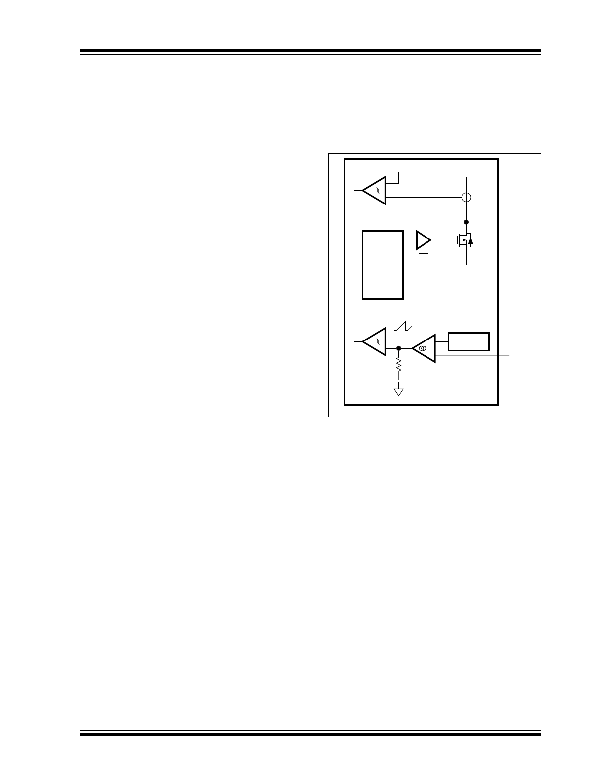
4.0 DETAILED DESCRIPTION
4.1 Bias Generator
The internal bias generator controls three voltage rails.
Two fixed-output low-dropout linear regulators, an
adjustable buck switch-mode power converter and an
unregulated charge pump are controlled through the
bias generator. In addition, the bias generator performs
supervisory functions.
4.1.1 +12V LOW-DROPOUT LINEAR
REGULATOR (LDO)
The +12V rail is used for bias of the 3-phase power
MOSFET bridge.
The regulator is capable of supplying 30 mA of external
load current. The regulator has a minimum overcurrent
limit of 40 mA.
When operating at a supply voltage (V
range of +12V to +12.7V, the +12V charge pump will be
off and the +12V source will be the VDD supply voltage.
The +12V output may be lower than +12V while
operating in the V
range of +12V to +12.7V due to
DD
the dropout voltage of the regulator.
The low-dropout regulators require an output capacitor
connected from V
to GND to stabilize the internal
OUT
control loop. A minimum of 4.7 µF ceramic output
capacitance is required for the 12V LDO.
The +12V LDO is disabled when the Chip Enable (CE)
pin is not active.
Table 4-1 shows the faults that will also disable the
+12V LDO.
4.1.2 +5V LOW-DROPOUT LINEAR
REGULATOR (LDO)
The +5V LDO is used for bias of an external
microcontroller, the internal current sense amplifier and
the gate control logic.
The +5V LDO is capable of supplying 30 mA of external
load current. The regulator has a minimum overcurrent
limit of 40 mA. If additional external current is
required, the buck switch-mode power converter
should be utilized.
A minimum of 4.7 µF ceramic output capacitance is
required for the 5V LDO.
The +5V LDO is disabled when the system is in Sleep
mode. The +5V LDO is enabled in the MCP8025 and
disabled in the MCP8026 when in standby mode.
Table 4-1 shows the faults that will also disable the +5V
LDO.
4.1.3 BUCK SWITCH MODE POWER
SUPPLY (SMPS)
The SMPS is a high-efficiency, fixed-frequency,
step-down DC-DC converter. The SMPS provides all
the active functions for local DC-DC conversion with
fast transient response and accurate regulation.
) that is in the
DD
During normal operation of the buck power stage, Q1 is
repeatedly switched on and off with the on and off times
governed by the control circuit. This switching action
causes a train of pulses at the LX node which are
filtered by the L/C output filter to produce a DC output
voltage, V
. Figure 4-1 depicts the functional block
O
diagram of the SMPS.
FIGURE 4-1: SMPS Functional Block Diagram.
The SMPS is designed to operate in Discontinuous
Conduction Mode (DCM) with Voltage mode control
and current-limit protection. The SMPS is capable of
supplying 750 mW of power to an external load at a
fixed switching frequency of 460 kHz with an input
voltage of 6V. The output of the SMPS is power-limited.
For a programmed output voltage of 3V, the SMPS will
be capable of supplying 250 mA to an external load. An
external diode is required between the LX pin and
ground. The diode will be required to handle the
inductor current when the switch is off. The diode is
external to the device to reduce substrate currents and
power dissipation caused by the switcher. The external
diode carries the current during the switch-off time,
eliminating the current path back through the device.
2014 Microchip Technology Inc. DS20005339A-page 29
Page 30

MCP8025/6
L
MAX
VO1
V
O
V
IN
--------–
T
2I
OCRIT
----------------------------------------------
The SMPS enters Pulse Frequency Modulation (PFM)
mode at light loads, improving efficiency at the expense
of higher output voltage ripple. The PFM circuitry
provides a means to disable the SMPS as well. If the
SMPS is not utilized in the application, connecting the
feedback pin (FB) to an external supply (2.5V to 5.5V)
will force the SMPS to a shutdown state.
The maximum inductor value for operation in
Discontinuous Conduction mode can be determined by
using Equation 4-1.
EQUATION 4-1: L
Using the L
inductor value calculated using
MAX
SIMPLIFIED
MAX
Equation 4-1 will ensure Discontinuous Conduction
mode operation for output load currents below the
critical current level, I
. For example, with an
O(CRIT)
output voltage of +5V, a standard inductor value of
4.7 µH will ensure Discontinuous Conduction mode
operation with an input voltage of 6V, a switching
frequency of 468 kHz and a critical load current of
150 mA.
The output voltage is set by using a resistor divider
network. The resistor divider is connected between the
inductor output and ground. The divider common point
is connected to the FB pin which is then compared to
an internal 1.25V reference voltage.
The buck regulator will set the BIOCPW bit in the STAT0
register and send a STATUS_0 message to the host
whenever the input switching current exceeds 2.5A
peak (typical). The bit will be cleared when the peak
input switching current drops back below the 2.5A
(typical) limit. This is a warning bit only, no action is
taken to shut down the buck operation. The overcurrent
limit will shorten the buck duty cycle and therefore limit
the maximum power out of the buck regulator.
The buck regulator will set the BUVLOW bit in the STAT0
register and send a STATUS_0 message to the host
whenever the output voltage drops below 90% of the
rated output voltage. The bit will be cleared when the
output voltage returns to 94% of the rated value.
If the buck regulator output voltage falls below 80% of
rated output voltage, the device will shut down with a
Buck Undervoltage Lockout Fault. The BUVLOF bit in
the STAT0 register will be set and a STATUS_0
message will be sent to the host. The ILIMIT_OUT
signal will transition low to indicate the fault.
The Voltage Supervisor is designed to shut down the
buck regulator when V
rises above AOVLO
DD
STOP
When shutting down the buck regulator is not
desirable, the user should add a voltage suppression
device to the V
rising above AOVLO
input in order to prevent VDD from
DD
STOP
.
The Voltage Supervisor is also designed to shut down
the buck regulator when V
UVLO
BK_STOP
.
falls below
DD
The device will set the BUVLOF bit in the STAT0 register
and send a STATUS_0 message to the host when the
buck input voltage drops below UVLO
BK_STOP
.
Table 4-1 shows the faults that will disable the buck
regulator.
4.1.4 CHARGE PUMP
An unregulated charge pump is utilized to boost the
input to the +12V LDO during low input conditions.
When the input bias to the device (VDD) drops below
CP
activated, 2 x V
, the charge pump is activated. When
START
is presented to the input of the +12V
DD
LDO, which maintains a minimum of +10V at its output.
The typical charge pump flying capacitor is a 0.1 µF to
1.0 µF ceramic capacitor.
4.1.5 SUPERVISOR
The bias generator incorporates a voltage supervisor
and a temperature supervisor.
4.1.5.1 Brown Out - Configuration Lost
When the device first powers up or when VDD drops
below 3.8V, the brown-out reset warning flag bit
(BORW) in the STAT1 register will be set. The bit is only
a warning indicating that the contents of the configuration registers may have been compromised by a low
supply voltage condition. The host processor should
send new configuration information to the device.
4.1.5.2 Voltage Supervisor
The voltage supervisor protects the device, the
external power MOSFETs and the external
microcontroller from damage caused by overvoltage or
undervoltage of the input supply, V
In the event of an undervoltage condition
< +5.5V) or an overvoltage condition of the
(V
DD
MCP8025 device (V
> +20V), the motor drivers are
DD
switched off. The bias generator, the communication
port and the remainder of the motor control unit remain
active. The failure state is flagged on the DE2 pin with
a status message. In extreme overvoltage conditions
> +32V), all functions are turned off.
(V
DD
In the event of a severe undervoltage condition
< +4.0V), the buck regulator will be disabled. If
(V
DD
the set point of the buck regulator output voltage is
above the buck undervoltage lockout value, the buck
output voltage will decrease as V
.
4.1.5.3 Temperature Supervisor
An integrated temperature sensor self-protects the
device circuitry. If the temperature rises above the
overtemperature shutdown threshold, all functions are
.
DD
decreases.
DD
DS20005339A-page 30 2014 Microchip Technology Inc.
Page 31

MCP8025/6
turned off. Active operation resumes when the
temperature has cooled down below a set hysteresis
value and the fault has been cleared by toggling CE.
It is desirable to signal the microcontroller with a
warning message before the overtemperature
threshold is reached. When the Thermal Warning
Temperature set point is exceeded, a warning message
will be sent to the host microcontroller. The
microcontroller should take appropriate actions to
reduce the temperature rise. The method to signal the
microcontroller is through the DE2 pin.
4.1.5.4 Internal Function Block Status
Table 4-1 shows the effects of the CE pin, the faults and
the Sleep bit upon the functional status of the internal
blocks of the MCP8025/6.
TABLE 4-1: INTERNAL FUNCTION BLOCK STATUS
System State Fault Conditions
Sleep CE = 0, SLEEP = 1 ——W——— —
Standby
CE = 0, SLEEP = 0 AAR——A A
(MCP8025)
Standby
CE = 0, SLEEP = 0 —A A——A A
(MCP8026)
Operating CE = 1, I
Faults
CE = 1,
LIMIT_OUT = 0
I
Driver OTP T
VDD UVLO VIN 5.5V — A ——— A A
Buck Input UVLO VIN 4V ————— A A
Buck Output Brownout V
5V LDO UVLO V
BUCK
LIMIT_OUT = 1 AAAAAA A
>160°C ————— A A
J
< 80% (Brownout) — A — — — A A
4V A A R A — A A
OUT5
Driver OVLO (MCP8025) VIN 20V AAAA—A A
32V ————— A A
IN
<8V, V
<8V AAAA—A A
LS[A:C]
>EXTOC<1:0> settingAAAA—A A
Input>2.5A Peak AAAAAA A
<90% AAAAAA A
V
BUCK
>72% T
J
SD_MIN
Warnings
CE = 1,
LIMIT_OUT = 1
I
System OVLO V
MOSFET UVLO V
MOSFET OCP V
Buck OCP I
HS[A:C]
Drain-Source
BUCK
Buck Output
Undervoltage
Driver Temperature T
(115°C for 160°C Driver OTP)
Config Lost (BORW) Set at initial power-up
or when V
<UVLO
DD
BK_STOP
Legend: “A” = ACTIVE (ON), “—” = INACTIVE (OFF), “W” = WAKEUP (from Sleep), “R” = RECEIVER ONLY
OCP = Overcurrent Protection
OTP = Overtemperature Protection
UVLO = Undervoltage Lockout
OVLO = Overvoltage Lockout
Buck
5V LDO
12V LDO
Motor Drivers
LIN, HV_IN1, HV_IN2
AAAAAA A
AAAAAA A
DE2
Internal
UVLO, OVLO, OTP
2014 Microchip Technology Inc. DS20005339A-page 31
Page 32

MCP8025/6
NEUTRAL
AB
C++
3
--------------------------------------- -=
4.2 Motor Control Unit
The motor control unit is comprised of the following:
• External drive for a 3-phase bridge with
NMOS/NMOS MOSFET pairs
• Back EMF sampler with phase multiplexer and
neutral simulator (MCP8025)
• Motor current sense amplifier and comparator
• Two additional current sense amplifiers
(MCP8026)
4.2.1 MOTOR CURRENT SENSE
CIRCUITRY
The internal motor current sense circuitry consists of an
operational amplifier and a comparator. The amplifier
output is presented to the inverting comparator input
and as an output to the microcontroller. The
non-inverting comparator input is connected to an
internally programmable 8-bit DAC. A selectable motor
current limit threshold may be set with a SET_ILIMIT
message from the host to the MCP8025/6 via the DE2
communication link. The DACREF<7:0> bits in the
CFG1 register contain the DAC current reference
value. The dual-purpose ILIMIT_OUT
current limit output as well as system fault outputs. The
8-bit DAC is powered by the 5V supply. The DAC
output voltage ranges from 0.991V to 4.503V. The DAC
has a bit value of (4.503V – 0.991V)/(2
1) = 13.77 mV/bit. A DAC input of 00H yields a DAC
output voltage of 0.991V. The default power-up DAC
value is 40H (1.872V). The DAC uses a 100 kHz filter.
Input code to output voltage delay is approximately five
time constants ~= 50 µs. The desired current sense
gain is established with an external resistor network.
Note: The motor current limit comparator output
is internally ‘OR’d with the DRIVER
FAULT output of the driver logic block.
The microcontroller should monitor the
comparator output and take appropriate
actions. The motor current limit
comparator circuitry does not disable the
motor drivers when an overcurrent
situation occurs. Only one current limit
comparator is provided. The MCP8026
provides three current sense amplifiers
which can be used for implementation of
advanced control algorithms, such as
Field-Oriented Control (FOC).
The comparator output may be employed as a current
limit. Alternatively, the current sense output can be
employed in a chop-chop PWM speed loop for any
situations where the motor is being accelerated, either
positively or negatively. An analog chop-chop speed
loop can be implemented by hysteretic control or fixed
off-time of the motor current. This makes for a very
robust controller, as the motor current is always in
instantaneous control.
pin handles the
8
A sense resistor in series with the bridge ground return
provides a current signal for both feedback and current
limiting. This resistor should be non-inductive to
minimize ringing from high di/dt. Any inductance in the
power circuit represents potential problems in the form
of additional voltage stress and ringing, as well as
increasing switching times. While impractical to
eliminate, careful layout and bypassing will minimize
these effects. The output stage should be as compact
as heat sinking will allow, with wide, short traces
carrying all pulsed currents. Each half-bridge should be
separately bypassed with a low ESR/ESL capacitor,
decoupling it from the rest of the circuit. Some layouts
will allow the input filter capacitor to be split into three
smaller values and serve double duty as the half-bridge
bypass capacitors.
Note: With a chop-chop control, motor current
always flows through the sense resistor.
When the PWM is off, however, the
flyback diodes or synchronous rectifiers
conduct, causing the current to reverse
polarity through the sense resistor.
The current sense resistor is chosen to establish the
peak current limit threshold, which is typically set 20%
higher than the maximum current command level to
provide overcurrent protection during abnormal
–
conditions. Under normal circumstances with a
properly compensated current loop, peak current limit
will not be exercised.
The current sense operational amplifier is disabled
when CE = 0.
4.2.2 BACK EMF SAMPLER WITH PHASE
MULTIPLEXER AND NEUTRAL
SIMULATOR (MCP8025)
The commutation loop of a BLDC motor control is a
phase locked loop (PLL), which locks to the rotor’s
position. Note that this inner loop does not attempt to
modify the position of the rotor, but modifies the
commutation times to match whatever position the
rotor has. An outer speed loop changes the rotor
velocity and the commutation loop locks to the rotor’s
position to commutate the phases at the correct times.
The back EMF sensor consists of the motor, a back
EMF sampler, a phase multiplexer and a neutral
simulator.
The back EMF sampler takes the motor phase voltages
and calculates the neutral point of the motor by using
Equation 4-2.
EQUATION 4-2: NEUTRAL POINT
DS20005339A-page 32 2014 Microchip Technology Inc.
Page 33

MCP8025/6
This allows the microcontroller to compare the back
EMF signal to the motor’s neutral point without the
need to bring out an extra wire on a WYE wound motor.
For DELTA wound motors, there is no physical neutral
to bring out, so this reference point must be calculated
in any case.
The back EMF sampler measures the motor phase that
is not driven, i.e. if LSA and HSB are on, then phase A
is driven low, phase B is driven high and phase C is
sampled. The sampled phase provides a back EMF
signal that is compared against the neutral of the motor.
The sampler is controlled by the microcontroller via the
MUX1 and MUX2 input signals.
When the BEMF signal crosses the neutral point, the
zero-crossing detector will switch the ZC_OUT signal.
The host controller may use this signal as a
30 degrees-before-commutation reference point. The
host controller must commutate the system after
30 degrees of electrical rotation have occurred.
Different motor control scenarios may increase or
decrease the commutation point by a few degrees.
Internal filtering capacitors are connected after the
phase voltage dividers to help eliminate transients
during the zero-crossing detection.
T ABLE 4-2: PHASE SAMPLER
MUX
Phase Sampled
MUX2 MUX1
0 0 PHASE A
0 1 PHASE B
1 0 PHASE C
1 1 PHASE C
The neutral simulator may be disabled when access to
the motor winding neutral point is available. When
disabling the neutral simulator, the motor neutral is
connected directly to the COMP_REF pin. The actual
motor neutral is then used for zero-crossing detection.
The neutral simulator may be disabled via DE2
communications.
4.2.3 MOTOR CONTROL
The commutation loop of a BLDC motor control is a
phase lock loop (PLL) which locks to the rotor’s
position. Note that this inner loop does not attempt to
modify the position of the rotor, but modifies the
commutation times to match whatever position the
rotor has. An outer speed loop changes the rotor
velocity and the commutation loop locks to the rotor’s
position to commutate the phases at the correct times.
4.2.3.1 Sensorless Motor Control
Many control algorithms can be implemented with the
MCP8025/6 in conjunction with a microcontroller. The
following discussion provides a starting point for
implementing the MCP8025 or MCP8026 in a
sensorless control application of a 3-phase motor. The
motor is driven by energizing two windings at a time
and sequencing the windings in a
six-step-per-electrical-revolution method. This method
leaves one winding unenergized at all times and the
voltage (Back EMF or BEMF) on that unenergized
winding can be monitored to determine the rotor
position.
4.2.3.2 Start-Up Sequence
When the motor being driven is at rest, the BEMF
voltage is equal to zero. The motor needs to be rotating
for the BEMF sensor to lock onto the rotor position and
commutate the motor. The recommended start-up
sequence is to bring the rotor from rest up to a speed
fast enough to allow BEMF sensing. Motor operation is
comprised of five modes: Disabled mode, Bootstrap
mode, Lock or Align mode, Ramp mode and Run
mode. Refer to the commutation state machine in
Table 4-3. The order in which the microcontroller steps
through the commutation state machine determines the
direction the motor rotates.
Disabled Mode (CE = 0)
When the driver is disabled (CE = 0), all of the
MOSFET driver outputs are set low.
Bootstrap Mode
The high-side driver obtains the high-side biasing
voltage from the 12V LDO, the bootstrap diode and the
bootstrap capacitor. The bootstrap capacitors must first
be charged before the high-side drives may be used.
The bootstrap capacitors are all charged by activating
all three low-side drivers. The active low-side drivers
pull their respective phase nodes low, charging the
bootstrap capacitors to the 12V LDO voltage. The three
low-side drivers should be active for at least 1.2 ms per
1 µf of bootstrap capacitance. This assumes a 12V
voltage change and 30 mA (10 mA per phase) of
current coming from the 12V LDO.
Lock Mode
Before the motor can be started, the rotor should be in
a known position. In Lock mode, the microcontroller
drives phase B low and phases A and C high. This
aligns the rotor 30 electrical degrees before the center
of the first commutation state. Lock mode must last
long enough to allow the motor and its load to settle into
this position.
2014 Microchip Technology Inc. DS20005339A-page 33
Page 34

MCP8025/6
Ramp Mode
At the end of the Lock mode, Ramp mode is entered. In
Ramp mode, the microcontroller steps through the
commutation state machine, increasing linearly, until a
minimum speed is reached. Ramp mode is an
open-loop commutation. No knowledge of the rotor
position is used.
Run Mode
At the end of Ramp mode, Run mode is entered. In Run
mode, the back EMF sensor is enabled and
commutation is now under the control of the phase lock
loop. Motor speed can be regulated by an outer speed
control loop.
TABLE 4-3: COMMUTATION STATE MACHINE
State
HSA HSB HSC LSA LSB LSC
CE = 0 OFF OFF OFF OFF OFF OFF N/A
BOOTSTRAP OFF OFF OFF ON ON ON N/A
LOCK ON OFF ON OFF ON OFF N/A
1 ON OFF OFF OFF OFF ON Phase B
2 OFF ON OFF OFF OFF ON Phase A
3 OFF ON OFF ON OFF OFF Phase C
4 OFF OFF ON ON OFF OFF Phase B
5 OFF OFF ON OFF ON OFF Phase A
6 ON OFF OFF OFF ON OFF Phase C
4.2.3.3 PWM Speed Control
The inner commutation loop is a phase-lock loop,
which locks to the rotor’s position. This inner loop does
not attempt to modify the position of the rotor, but
modifies the commutation times to match whatever
position the rotor has. The outer speed loop changes
the rotor velocity and the inner commutation loop locks
to the rotor’s position to commutate the phase at the
correct times.
The outer speed loop pulse width modulates the motor
drive inverter to produce the desired wave shape and
voltage at the motor. The inductance of the motor then
integrates this pulse-width modulation (PWM) pattern
to produce the desired average current, thus controlling
the desired torque and speed of the motor. For a
trapezoidal BLDC motor drive with six-step
commutation, the PWM is used to generate the
average voltage to produce the desired motor current
and motor speed.
There are two basic methods to pulse-width modulate
the inverter switches. The first method returns the
reactive energy in the motor inductance to the source
by reversing the voltage on the motor winding during
the current decay period. This method is referred to as
fast decay or chop-chop. The second method
circulates the reactive current in the motor with minimal
voltage applied to the inductance. This method is
referred to as slow decay or chop-coast.
Outputs
The preferred control method employs a chop-chop
PWM for any situation where the motor is being
accelerated, either positively or negatively. For
improved efficiency, chop-coast PWM is employed
during steady-state conditions. The chop-chop speed
loop is implemented by hysteretic control, fixed off-time
control or average current mode control of the motor
current. This makes for a very robust controller, as the
motor current is always in instantaneous control.
The motor speed presented to the chop-chop loop is
reduced by approximately 9%. A fixed-frequency PWM
that only modulates the high-side switches implements
the chop-coast loop. The chop-coast loop is presented
with the full motor speed, so, if it is able to control the
speed, the chop-chop loop will never be satisfied and
will remain saturated. The chop-chop remains able to
assume full control if the motor torque is exceeded,
either through a load change or a change in speed that
produces acceleration torque. The chop-coast loop will
remain saturated, with the chop-chop loop in full
control, during start-up and acceleration to full speed.
The bandwidth of the chop-coast loop is set to be
slower than the chop-chop loop so that any transients
will be handled by the chop-chop loop and the
chop-coast loop will only be active in steady-state
operation.
BEMF
Phase
DS20005339A-page 34 2014 Microchip Technology Inc.
Page 35

MCP8025/6
4.2.4 EXTERNAL DRIVE FOR A 3-PHASE
BRIDGE WITH NMOS/NMOS
MOSFET PAIRS
Each motor phase is driven with external
NMOS/NMOS MOSFET pairs. These are controlled by
a low-side and a high-side gate driver. The gate drivers
are controlled directly by the digital input pins
PWM[1:3]H/L. A logic high turns the associated gate
driver ON and a logic low turns the associated gate
driver OFF. The PWM[1:3]H/L digital inputs are
equipped with internal pull-down resistors.
The low-side gate drivers are biased by the +12V LDO
output, referenced to ground. The high-side gate
drivers are a floating drive biased by a bootstrap
capacitor circuit. The bootstrap capacitor is charged by
the +12V LDO whenever the accompanying low-side
MOSFET is turned on.
The high-side and low-side driver outputs all go to a low
state whenever there is a fault or when CE = 0,
regardless of the PWM[1:3]H/L inputs.
4.2.4.1 MOSFET Driver External Protection
Features
Each driver is equipped with Undervoltage Lockout
(UVLO) and short circuit protection features.
4.2.4.1.1 MOSFET Driver Undervoltage Lockout
(UVLO)
The MOSFET UVLO fault detection monitors the
available voltage used to drive the external MOSFET
gates. The fault detection is only active while the driver
is actively driving the external MOSFET gate. Anytime
the driver bias voltage is below the Driver Undervoltage
Lockout (D
one specified by the t
not turn ON when commanded ON. A driver fault will be
indicated to the host microcontroller on the
ILIMIT_OUT
communication Status_1 message. This is a latched
fault. Clearing the fault requires either removal of
device power or disabling and re-enabling the device
via the device enable input (CE). The EXTUVLO bit in
the CFG0 register is used to enable or disable the
Driver Undervoltage Lockout feature. This protection
feature prevents the external MOSFETs from being
controlled with a gate voltage not suitable to fully
enhance the device.
) threshold for a period longer than the
UVLO
open-drain output pin and also via a DE2
parameter, the driver will
DUVLO
4.2.4.1.2 External MOSFET Short Circuit Current
Short circuit protection monitors the voltage across the
external MOSFETs during an ON condition. The
high-side driver voltage is measured from V
PH[1:3]. The low-side driver voltage is measured from
PH[1:3] to ground. If the voltage rises above a
user-configurable threshold after the external MOSFET
gate voltage has been driven high, all drivers will be
turned OFF. A driver fault will be indicated to the host
microcontroller on the open-drain ILIMIT_OUT
pin and also via a DE2 communication Status_1
message. This is a latched fault. Clearing the fault
requires either removal of device power or disabling
and re-enabling the device via the device enable input
(CE). This protection feature helps detect internal
motor failures such as winding to case shorts.
Note: The driver short circuit protection is
dependent on application parameters. A
configuration message is provided for a
set number of threshold levels. The
MOSFET Driver UVLO and short circuit
protection features have the option to be
disabled.
The short circuit voltage may be set via a DE2
Set_Cfg_0 message. The EXTOC<1:0> bits in the
CFG0 register are used to select the voltage level for
the short circuit comparison. If the voltage across the
MOSFET drain-source terminals exceeds the selected
voltage level when the MOSFET is active, a fault will be
triggered. The selectable voltage levels are 250 mV,
500 mV, 750 mV and 1000 mV. The EXTSC bit in the
CFG0 register is used to enable or disable the
MOSFET driver short circuit detection.
4.2.4.1.3 Fault Pin Output (ILIMIT_OUT
The dual purpose ILIMIT_OUT pin is used as a fault
indicator and as an overcurrent indicator when used
with the internal DAC. The pin is capable of sinking a
minimum of 1 mA of current while maintaining less than
50 mV of voltage across the output. An external pull-up
resistor to the logic supply is required.
The open-drain ILIMIT_OUT
fault occurs. Table 4-4 lists the faults that activate the
ILIMIT_OUT signal. Warnings do not activate the
ILIMIT_OUT
signal. Table 4-5 lists the warnings.
pin transitions low when a
)
to
DD
output
2014 Microchip Technology Inc. DS20005339A-page 35
Page 36
MCP8025/6
TABLE 4-4: ILIMIT_OUT FAULTS
Fault DE2 Register
Overtemperature 0x85 0x02
Device Input Undervoltage 0x85 0x04
Driver Input Overvoltage 0x85 0x08
Device Input Overvoltage 0x85 0x10
Buck Regulator Output Undervoltage 0x85 0x80
External MOSFET Undervoltage
Lockout
External MOSFET Overcurrent
Detection
5V LDO Undervoltage Lockout 0x86 0x20
0x86 0x04
0x86 0x08
TABLE 4-5: WARNINGS
Fault DE2 Register
Temperature Warning 0x85 0x01
Buck Regulator Overcurrent 0x85 0x20
Buck Regulator Undervoltage 0x85 0x40
Brownout – Configuration Lost 0x86 0x10
4.2.4.2 Gate Control Logic
The gate control logic provides level shifting of the
digital inputs, polarity control and cross conduction
protection.
4.2.4.2.1 Cross Conduction Protection
Logic prevents switching ON one power MOSFET
while the opposite one in the same half-bridge is
already switched ON. If both MOSFETs in the same
half-bridge are commanded ON simultaneously by the
digital inputs, both will be turned OFF.
4.2.4.2.2 Programmable Dead Time
The gate control logic employs a break-before-make
dead-time delay that is programmable. A configuration
message is provided to configure the driver dead time.
The programmable dead times range from 250 ns to
2000 ns (default) in 250 ns increments. The dead time
allows the PWM inputs to be direct inversions of each
other and still allow proper motor operation. The dead
time internally modifies the PWMH/L gate drive timing
to prevent cross conduction. The DRVDT<2:0> bits in
the CFG2 register are used to set the dead time value.
4.2.4.2.3 Programmable Blanking Time
A configuration message is provided to configure the
driver current limit blanking time. The blanking time
allows the system to ignore any current spikes that may
occur when switching the driver outputs. The allowable
blanking times are 500 ns, 1 µs, 2 µs and 4 µs
(default). The blanking time will start after the dead time
circuitry has timed out. The DRVBT<1:0> bits in the
CFG2 register are used to set the blanking time value.
The blanking time affects the driver undervoltage
lockout. The driver undervoltage lockout latches the
external MOSFET undervoltage lockout fault if the
undervoltage condition lasts longer than the time
specified by the t
parameter takes into account the blanking time if
blanking is in progress.
parameter. The t
DUVLO
DUVLO
4.3 Chip Enable (CE)
The Chip Enable (CE) pin allows the device to be
disabled by external control. The Chip Enable pin has
four modes of operation.
4.3.1 FAULT CLEARING STATE
The CE pin is used to clear any faults and re-enable the
driver. After toggling the CE pin low to high, the system
requires a minimum time period to re-enable and start
up all the driver blocks. The start-up time is
approximately 35 μs. The maximum pulse time for the
high-low-high transition to clear faults should be less
than 1 ms. If the high-low-high transition is longer than
1 ms, the device will start up from the Standby state.
Any fault status bits that are set will be cleared by the
low-to-high transition of the CE pin if, and only if, the
fault condition has ceased to exist. If the fault condition
still exists, the active fault status bit will remain active.
No additional fault messages will be sent for a fault that
remains active.
4.3.2 WAKE FROM SLEEP MODE
The CE pin is also used to awaken the device from the
Sleep mode state. To wake the device from a Sleep
mode state, the CE pin must be set low for a minimum
of 250 μs. The device will then wake up with the next
rising edge of the CE pin.
The LIN bus may be used to wake the device from the
Sleep mode state. When a LIN wake-up event is
detected on the LIN_BUS pin, the device will wake up.
The MCP8025 will wake up on the rising edge of the
bus after detecting a dominate state lasting > 150 µs
on the bus. The LIN Bus master must provide the
dominate state for > 250 µs to meet the LIN 2.2A
specifications.
The HV_IN1 pin may be used to wake the device from
the Sleep mode state. The MCP8026 will wake up on
the rising edge of the pin after detecting a low state
lasting > 250 µs on the pin.
DS20005339A-page 36 2014 Microchip Technology Inc.
Page 37

MCP8025/6
4.3.3 STANDBY STATE
Standby state is entered when the CE pin goes low for
longer than 1 ms and the Sleep configuration bit is
inactive. When Standby mode is entered, the following
subsystems are disabled:
• high-side gate drives (HSA, HSB, HSC), forced
low
• low-side gate drives (LSA, LSB, LSC), forced low
•12V LDO
•5V LDO (MCP8026)
• the 30 k pull-up resistor connected to the level
translator is switched out of the circuit to minimize
current consumption (configurable) (MCP8026)
• the 30 k pull-up resistor connected to the LIN
Bus is switched out of the circuit to minimize
current consumption (configurable) (MCP8025)
The buck regulator stays enabled. The DE2
communication port remains active but the port may
only respond to commands. When CE is inactive, the
DE2 port is prevented from initiating communications in
order to conserve power.
The total current consumption of the device when CE is
inactive (device disabled) stays within the Standby
mode input quiescent current limits specified in the
AC/DC Characteristics table.
4.3.4 SLEEP MODE
Sleep mode is entered when both a SLEEP command
is sent to the device via DE2 communication and the
CE pin is low. The two conditions may occur in any
order. The transition to Sleep mode occurs after the last
of the two conditions occurs and the t
has elapsed. The SLEEP bit in the CFG0 configuration
register indicates when the device should transition to
a low-power mode. The device will operate normally
until the CE pin is transitioned low by an external
device. At that point in time, the SLEEP bit value
determines whether the device transitions to Standby
mode or low-power Sleep mode. The quiescent current
during Sleep mode will typically be 5 μA. When Sleep
mode is activated, most functions will be shut off,
including the buck regulator. Only the power-on reset
monitor, the voltage translators and the minimal state
machine will remain active to detect a wake-up event.
This indicates that the host processor will be shut down
if the host is using the buck regulator for power. The
device will stay in the low-power Sleep mode until
either of the following conditions is met:
• The CE pin is toggled low for a minimum of 250 μs
and then transitioned high.
• The LIN_BUS pin receives a LIN wake-up event.
The wake-up event must last at least 250 µs, per LIN
Standard 2.2A. (MCP8025)
• The HV_IN1 pin transitions high after being in a low
state lasting longer than 250 µs. (MCP8026)
SLEEP
delay time
The MCP8025/6 devices are not required to retain
configuration data while in Sleep mode. Sleep mode
will set the BORW bit. When exiting Sleep mode, the
host should send a new configuration message to
configure the device if the default configuration values
are not desired. The same configuration sequence
used during power-up may be used when exiting Sleep
mode. Sleep mode will not be entered if there is a fault
active that will affect the buck regulator output voltage.
This prevents a transition to Sleep mode when the host
is powered by the buck regulator and the regulator is in
an unreliable state.
4.4 Communication Ports
The communication ports provide a means of
communicating to the host system.
4.4.1 LIN BUS TRANSCEIVER (MCP8025)
The MCP8025 provides a physical interface between a
microcontroller and a LIN half-duplex bus. It is intended
for automotive and industrial applications with serial
bus speeds up to 20 kilobaud. The MCP8025 provides
a half-duplex, bidirectional communication interface
between a microcontroller and the serial network bus.
This device will translate the CMOS/TTL logic levels to
LIN level logic and vice versa.
The LIN Bus transceiver circuit provides a LIN
Bus-compliant interface between the LIN Bus and a
LIN-capable UART on an external microcontroller. The
LIN Bus transceiver is load dump protected and
conforms to LIN 2.1.
4.4.1.1 LIN Wake-Up
A LIN wake-up event may be used to wake up the
MCP8025 from Sleep mode. The MCP8025 will wake
up on the rising edge of the LIN bus after detecting a
dominate state lasting > 150 µs on the LIN_BUS pin.
The LIN Bus master must provide the dominate state
for > 250 µs to meet the LIN 2.2A and SAE J2602.
4.4.1.2 FAULT/TXE (MCP8025)
The FAULT/TXE pin is a bidirectional open-drain output
pin. The state of the pin is defined in Tab le 4- 6.
Whenever the FAULT
transmitter is off. The transmitter may be re-enabled
whenever the FAULT/TXE signal returns high, either by
removing the internal fault condition or by the host
returning the FAULT
The FAULT
between the TX input and the LIN_BUS level. This may
be used to detect a bus contention.
/TXE will go low when there is a mismatch
/TXE signal is low, the LIN
/TXE high.
2014 Microchip Technology Inc. DS20005339A-page 37
Page 38

MCP8025/6
The FAULT/TXE pin will go low whenever the internal
circuits have detected a short circuit and have disabled
the LIN_BUS output driver. The MCP8025 limits the
transmitter current to less than 200 mA when a short
circuit is detected. If the host MCU is driving the
/TXE pin high, then the transmitter will remain
FAU LT
enabled and the fault condition will be overruled. If the
host MCU is driving the pin low or is in Hi-Z mode, the
MCP8025 will drive the pin low and will disable the LIN
transmitter.
4.4.1.3 LIN Dominant State Timeout
The MCP8025 has an additional LIN feature, LIN
Dominant State Timeout, that is not in the current LIN
2.0 specification. If the LIN TX pin is externally held low
for more than the time specified by t
MCP8025 will disable the LIN transmitter. The
/TXE pin will go low, indicating a LIN Dominant
FAULT
State Timeout fault. Forcing the FAULT
will not re-enable the transmitter. The transmitter will
stay disabled until the TX pin is set high again. This
prevents the LIN transceiver from inadvertently locking
up the bus.
TABLE 4-6: FAULT/TXE TRUTH TABLE
FAULT/TXE
TX
In
LH V
LH V
HH V
HL GNDHi-Z, HHOK, data is being received from the LIN_Bus
LL GNDHi-Z, HHOK
L L GND
xx V
Legend:x = don’t care
Note 1: The FAULT
RX
Out
reporting during bus propagation delays.
LIN_BUS
I/O
DD
DD
DD
V
DD
/TXE is valid approximately 25 µs after the TXD falling edge. This helps eliminate false fault
External
Input
Hi-Z L FAULT, TX driven low, LIN_BUS shorted to V
HLFAULT, Overridden by CPU driving FAULT/TXE high
Hi-Z, H H OK
Hi-Z, H L FAULT, if TX is low longer than t
DD
LxNO FAULT, the CPU is commanding the transceiver to
Driven
Output
Definition
DOM_TOUT
turn off the transmitter driver
DOM_TOUT
/TXE pin high
DD
, the
(Note 1)
4.4.2 LEVEL TRANSLATOR (MCP8026)
The level translators are an interface between the
companion microcontroller’s logic levels and the input
voltage levels from the system. Automotive
applications typically drive the inputs from the Engine
Control Unit (ECU) and the ignition key on/off signals.
The level translators are unidirectional translators.
Signals on the high-voltage input are translated to
low-voltage signals on the low-voltage outputs. The
high-voltage HV_IN[1:2] inputs have a configurable
30 k pull up. The pull up is configured via a
SET_CFG_0 message. The PU30K bit in the CFG0
register controls the state of the pull up. The bit may
only be changed when the CE pin is active. The
low-voltage LV_OUT[1:2] outputs are open-drain
outputs. The outputs are capable of sinking a minimum
of 1 mA of current while maintaining less than 50 mV at
the output.
The HV_IN1 translator is also used to wake up the
device from the Sleep mode whenever the HV_IN1
input is transitioned to a low level for a minimum of
250 µs followed by a transition to the high voltage level.
Note: The TQFP package has two level
translators. The second level translator
typically interfaces to an Ignition Key
on/off signal.
DS20005339A-page 38 2014 Microchip Technology Inc.
Page 39

MCP8025/6
4.4.3 DE2 COMMUNICATIONS PORT
A half-duplex 9600 baud UART interface is available to
communicate with an external host. The port is used to
configure the MCP8025/6 and also for status and fault
messages. The DE2 communication port is described
in detail in Section 4.4.3.1 “Communication
Interface”.
4.4.3.1 Communication Interface
A single-wire, half-duplex, 9600 baud, 8-bit
bidirectional communication interface is implemented
using the open-drain DE2 pin. The interface consists of
eight data bits, one Stop bit and one Start bit. The
implementation of the interface is described in the
following sections.
The DE2 interface is an open-drain interface. The
open-drain output is capable of sinking a minimum of
1 mA of current while maintaining less than 50 mV at
the output.
A 5 k resistor should typically be used between the
host transmit pin and the MCP8025/6 DE2 pin to allow
the MCP8025/6 to drive the DE2 line when the host TX
pin is at an idle high level.
The DE2 communication is active when CE = 0 with
the constraint that the MCP8025/6 devices will not
initiate any messages. The host processor may initiate
messages regardless of the state of the CE pin when
the device is not in Sleep mode. The MCP8025/6
devices will respond to host commands when the CE
pin is low. The time from receiving the last bit of a
command message to sending the first bit of the
response message ranges from DE2
corresponding to 0 µs to 3.125 ms.
RSP
to DE2
WAIT
4.4.3.3 Packet Timing
While no data is being transmitted, a logic ‘1’ must be
placed on the open-drain DE2 line by an external
pull-up resistor. A data packet is composed of one Start
bit, which is always a logic ‘0’, followed by eight data
bits and a Stop bit. The Stop bit must always be a logic
‘1’. It takes 10 bits to transmit a byte of data.
The device detects the Start bit by detecting the
transition from logic 1 to logic 0 (note that, while the
data line is idle, the logic level is high). Once the Start
bit is detected, the next data bit’s “center” can be
assured to be 24 ticks minus 2 (worst case
synchronizer uncertainty) later. From then on, every
next data bit center is 16 clock ticks later. Figure 4-3
illustrates this point.
4.4.3.4 Message Handling
The driver will not transition to Standby mode or Sleep
mode while a message is being received. If a message
arrives before the CE = 0 to Standby (or Sleep) mode
transition delay, t
driver will wait until the on-going message is completed
before changing modes.
STANDBY
(or t
), times out, the
SLEEP
4.4.3.2 Packet Format
Every internal status change will provide a
communication to the microcontroller. The interface
uses a standard UART baud rate of 9600 bits per
second.
In the DE2 protocol, the transmitter and the receiver do
not share a clock signal. A clock signal does not
emanate from one transmitter to the other receiver.
Due to this reason, the protocol is asynchronous. The
protocol uses only one line to communicate, so the
transmit/receive packet must be done in Half-Duplex
mode. A new transmit message is allowed only when a
complete packet has been transmitted.
The host must listen to the DE2 line in order to check
for contentions. In case of contention, the host must
release the line and wait for at least three packet-length
times before initiating a new transfer.
Figure 4-2 illustrates a basic DE2 data packet.
2014 Microchip Technology Inc. DS20005339A-page 39
Page 40
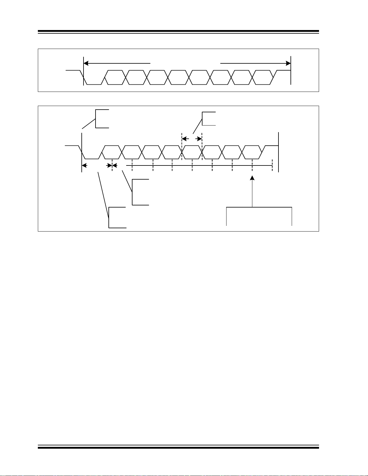
MCP8025/6
STOP
STARTDE2
Message Format
B
0
B
1
B
2
B
3
B
4
B
5
B
6
B
7
STOP
START
B
0
B
1
B
2
B
3
B
4
B
5
B
6
B
7
T
START
= 1.5T – uncertainty on start
Detection (worse case: 2x T
S
)
T
S
= T/16 (oversampled bit-cell period)
Receiver samples the incoming data
using x16 baud rate clock
Sample incoming data
at the bit-cell center
T
S
T
START
T
T = 1/Baud Rate (bit-cell period)
Detect start bit by sensing
transition from logic 1 to logic 0
worst
FIGURE 4-2: DE2 Packet Format.
FIGURE 4-3: DE2 Packet Timing.
4.4.4 MESSAGING INTERFACE
A command byte will always have the most significant
bit 7 (msb) set to ‘1’. Bits 6 and 5 are reserved for future
use and should be set to ‘0’. Bits 4 – 0 are used for
commands. That allows for 32 possible commands.
4.4.4.1 Host to MCP8025/6
Messages sent from the host to the MCP8025/6
devices consist of either one or two eight-bit bytes. The
first byte transmitted is the command byte. The second
byte transmitted, if required, is the data for the
command.
If a multi-byte command is sent to the MCP8025/6
devices and no second byte is received by the
MCP8025/6 devices, then a “Command Not
Acknowledged” message will be sent back to the host
after a 5 ms timeout period.
4.4.4.2 MCP8025/6 to Host
A solicited response byte from the MCP8025/6 devices
will always echo the command byte with bit 7 set to ‘0’
(Response) and with bit 6 set to ‘1’ for Acknowledged
(ACK) or ‘0’ for Not Acknowledged (NACK). The
second byte, if required, will be the data for the host
command. Any command that causes an error or is not
supported will receive a NACK response.
The MCP8025/6 devices may send unsolicited
command messages to the host controller. No
message to the host controller requires a response
from the host controller.
DS20005339A-page 40 2014 Microchip Technology Inc.
Page 41

MCP8025/6
4.4.5 MESSAGES
4.4.5.1
There is a SET_CFG_0 message that is sent by the
host to the MCP8025/6 devices to configure the
devices. The SET_CFG_0 message may be sent to the
device at any time. The host is responsible for making
sure the system is in a state that will not be
compromised by sending the SET_CFG_0 message.
The SET_CFG_0 message format is indicated in
Table 4-7. The response is indicated in Table 4-8.
SET_CFG_0
4.4.5.2 GET_CFG_0
There is a GET_CFG_0 message that is sent by the
host to the MCP8025/6 devices to retrieve the device
configuration register. The GET_CFG_0 message
format is indicated in Tab le 4- 7. The response is
indicated in Tab le 4- 8.
4.4.5.3 STATUS_0 and STATUS_1
There are STATUS_0 and STATUS_1 messages that
are sent by the host to the MCP8025/6 devices to
retrieve the device STAT0 or STAT1 register.
Unsolicited STATUS_0 and STATUS_1 messages may
also be sent to the host by the MCP8025/6 devices to
inform the host of status changes. The unsolicited
STATUS_0 and STATUS_1 messages will only be sent
when a status bit changes to an active state.
STATUS_0 and STATUS_1 message format is
indicated in Tab le 4 -7 . The response is indicated in
Table 4-8.
When a STATUS_0 or STATUS_1 message is sent to
the host in response to a new fault becoming active, the
fault bit will be cleared either by the host issuing a
STATUS_0 or STATUS_1 request message or by the
host toggling the CE pin low then high. The fault bit will
stay active and not be cleared if the fault condition still
exists at the time the host attempted to clear the fault.
The BORW bit in the STAT1 register will be set every
time the device restarts due to a brown-out event, a
Sleep mode wake-up or a normal power-up. When the
bit is set, a single unsolicited message will be sent to
the host indicating a voltage brown-out or power-up
has taken place and that the configuration data may
have been lost. The flag is reset by a “Status 1 Ack”
(01000110 (46H)) from the device in response to a
Host Status Request command.
The
4.4.5.5 GET_CFG_1
There is a GET_CFG_1 message that is sent by the
host to the MCP8025/6 devices to retrieve the motor
current limit reference DAC configuration register. The
GET_CFG_1 message format is indicated in Tab le 4 -7 .
The response is indicated in Ta bl e 4 -8 .
4.4.5.6 SET_CFG_2
There is a SET_CFG_2 message that is sent by the
host to the MCP8025/6 devices to configure the driver
current limit blanking time. The SET_CFG_2 message
may be sent to the device at any time. The host is
responsible for making sure the system is in a state that
will not be compromised by sending the SET_CFG_2
message. The SET_CFG_2 message format is
indicated in Tab le 4 -7 . The response is indicated in
Table 4-8.
4.4.5.7 GET_CFG_2
There is a GET_CFG_2 message that is sent by the
host to the MCP8025/6 devices to retrieve the device
Configuration Register 2. The GET_CFG_2 message
format is indicated in Tab le 4 -7 . The response is
indicated in Ta bl e 4 -8 .
4.4.5.4 SET_CFG_1
There is a SET_CFG_1 message that is sent by the
host to the MCP8025/6 devices to configure the motor
current limit reference DAC. The SET_CFG_1 message
may be sent to the device at any time. The host is
responsible for making sure the system is in a state that
will not be compromised by sending the SET_CFG_1
message. The SET_CFG_1 message format is
indicated in Tab le 4 -7 . The response is indicated in
Table 4-8.
2014 Microchip Technology Inc. DS20005339A-page 41
Page 42

MCP8025/6
TABLE 4-7: DE2 COMMUNICATION COMMANDS TO MCP8025/6 FROM HOST
Command Byte Bit Value Description
SET_CFG_0
GET_CFG_0 1 10000010 (82H) Get Configuration Register 0
SET_CFG_1 1 10000011 (83H) Set Configuration Register 1
GET_CFG_1 1 10000100 (84H) Get Configuration Register 1
STATUS_0 1 10000101 (85H) Get Status Register 0
STATUS_1 1 10000110 (86H) Get Status Register 1
SET_CFG_2 1 10000111 (87H) Set Configuration register 2
GET_CFG_2 1 10001000 (88H) Get Configuration Register 2
1 10000001b (81H) Set Configuration Register 0
27
6
5 0 System Enters Standby Mode when CE = 0
4
3
2
1:0
2 7:0 00H – FFH Select DAC Current Reference value.
27:5
4:2
1:0
0 Reserved
-- (Always ‘0’ in SLEEP mode)
0 Enable Disconnect of 30 k LIN Bus/Level Translator Pull Up when
CE =
0 (Default)
1 Disable Disconnect of 30 k LIN Bus/Level Translator Pull Up when
CE =
0
1
0 Disable Internal Neutral Simulator (Start-Up Default)
1 Enable Internal Neutral Simulator
0 Enable MOSFET Undervoltage Lockout (Start-Up Default)
1 Disable MOSFET Undervoltage Lockout
0 Enable External MOSFET Short Circuit Detection (Start-Up Default)
1 Disable External MOSFET Short Circuit Detection
00 Set External MOSFET Overcurrent Limit to 0.250V (Start-Up Default)
01 Set External MOSFET Overcurrent Limit to 0.500V
10 Set External MOSFET Overcurrent Limit to 0.750V
11 Set External MOSFET Overcurrent Limit to 1.000V
00H Reserved
— Driver Dead Time (for PWMH/PWML inputs)
000 2000 ns (Default)
001 1750 ns
010 1500 ns
011 1250 ns
100 1000 ns
101 750 ns
110 500 ns
111 250 ns
— Driver Blanking Time (Ignore Switching Current Spikes)
00 4 µs (Default)
01 2µs
10 1µs
11 500 ns
System Enters Sleep Mode when CE = 0, 30 k LIN Bus/Level
Translator Pull Up Disconnect Always Enabled
DAC Motor Current Limit Reference Voltage
(4.503V – 0.991V)/255 = 13.77 mV/bit
00H = 0.991V
40H = 1.872V (40H x 0.1377 mV/bit + 0.991V) (Start-Up Default)
FFH = 4.503V (FFH x 0.1377 mV/bit + 0.991V)
Get DAC Motor Current Limit Reference Voltage
DS20005339A-page 42 2014 Microchip Technology Inc.
Page 43

MCP8025/6
TABLE 4-8: DE2 COMMUNICATION MESSAGES FROM MCP8025/6 TO HOST
MESSAGE BYTE BIT VALUE DESCRIPTION
SET_CFG_0 17:000000001 (01H) Set Configuration Register 0 Not Acknowledged (Response)
01000001 (41H) Set Configuration Register 0 Acknowledged (Response)
27 0 Reserved
6 — Ignored in SLEEP mode
0 Enable Disconnect of 30K LIN Bus/Level Translator Pull Up when
CE = 0 (Default)
1 Disable Disconnect of 30K LIN Bus/Level Translator Pull Up when
CE = 0
5 0 System Enters Standby Mode when CE = 0
1 System Enters Sleep Mode when CE = 0, 30k LIN Bus/Level
Translator Pull Up Disconnect Always Enabled
4 0 Internal Neutral Simulator Disabled (Start-Up Default)
1 Internal Neutral Simulator Enabled
3 0 Undervoltage Lockout Enabled (Default)
1 Undervoltage Lockout Disabled
2 0 External MOSFET Overcurrent Detection Enabled (Default)
1 External MOSFET Overcurrent Detection Disabled
1:0 00 0.250V External MOSFET Overcurrent Limit (Default)
01 0.500V External MOSFET Overcurrent Limit
10 0.750V External MOSFET Overcurrent Limit
11 1.000V External MOSFET Overcurrent Limit
GET_CFG_0 17:000000010 (02H) Get Configuration Register 0 Response Not Acknowledged (Response)
01000010 (42H) Get Configuration Register 0 Response Acknowledged (Response)
27 0 Reserved
6 -- Ignored in SLEEP mode
0 Enable Disconnect of 30K LIN Bus/Level Translator Pull Up when
CE = 0 (Default)
1 Disable Disconnect of 30K LIN Bus/Level Translator Pull Up when
CE = 0
5 0 System Enters Standby Mode when CE = 0
1 System Enters Sleep Mode when CE = 0, 30k LIN Bus/Level
Translator Pull Up Disconnect Always Enabled.
4 0 Internal Neutral Simulator Disabled (Start-Up Default)
1 Internal Neutral Simulator Enabled
3 0 Undervoltage Lockout Enabled
1 Undervoltage Lockout Disabled
2 0 External MOSFET Overcurrent Detection Enabled
1 External MOSFET Overcurrent Detection Disabled
1:0
00 0.250V External MOSFET Overcurrent Limit
01 0.500V External MOSFET Overcurrent Limit
10 0.750V External MOSFET Overcurrent Limit
11 1.000V External MOSFET Overcurrent Limit
2014 Microchip Technology Inc. DS20005339A-page 43
Page 44

MCP8025/6
TABLE 4-8: DE2 COMMUNICATION MESSAGES FROM MCP8025/6 TO HOST (CONTINUED)
MESSAGE BYTE BIT VALUE DESCRIPTION
SET_CFG_1 1 00000011 (03H) Set DAC Motor Current Limit Reference Voltage Not Acknowledged
(Response)
01000011 (43H) Set DAC Motor Current Limit Reference Voltage Acknowledged
(Response)
2 7:0 00H – FFH Current DAC Current Reference Value: 13.77 mV/bit + 0.991V
GET_CFG_1 1 00000100 (04H) Get DAC Motor Current Limit Reference Voltage Not Acknowledged
(Response)
01000100 (44H) Get DAC Motor Current Limit Reference Voltage Acknowledged
(Response)
2 7:0 00H – FFH Current DAC Current Reference Value: 13.77 mV/bit + 0.991V
STATUS_0 17:000000101 (05H) Status Register 0 Response Not Acknowledged (Response)
01000101 (45H) Status Register 0 Response Acknowledged (Response)
10000101 (85H) Status Register 0 Command to Host (Unsolicited)
27:0 00000000 Normal Operation
00000001 Temperature Warning (T
00000010 Overtemperature (TJ> 160°C)
00000100 Input Undervoltage (VDD<5.5V)
00001000 Driver Input Overvoltage (20V < V
00010000 Input Overvoltage (VDD> 32V)
00100000 Buck Regulator Overcurrent
01000000 Buck Regulator Output Undervoltage Warning
10000000 Buck Regulator Output Undervoltage (< 80%, Brown-Out Error)
STATUS_1 17:000000110 (06H) Status Register 1 Response Not Acknowledged (Response)
01000110 (46H) Status Register 1 Response Acknowledged (Response)
10000110 (86H) Status Register 1 Command to Host (Unsolicited)
27:0 00000000 Normal Operation
00000001 Reserved
00000010 Reserved
00000100 External MOSFET Undervoltage Lockout (UVLO)
00001000 External MOSFET Overcurrent Detection
00010000 Brown-Out Reset – Config Lost (Start-Up Default = 1)
00100000 5V LDO Undervoltage Lockout (UVLO)
01000000 Reserved
10000000 Reserved
> 72% T
J
DDH
= 115°C) (Default)
SD_MIN
< 32V)
DS20005339A-page 44 2014 Microchip Technology Inc.
Page 45
MCP8025/6
TABLE 4-8: DE2 COMMUNICATION MESSAGES FROM MCP8025/6 TO HOST (CONTINUED)
MESSAGE BYTE BIT VALUE DESCRIPTION
SET_CFG_2 1 00000111 (07H) Set Configuration Register 2 Not Acknowledged (Response)
01000111 (47H) Set Configuration Register 2 Acknowledged (Response)
27:5 00H Reserved
4:2 — Driver Dead Time (for PWMH/PWML inputs)
000 2000 ns (Default)
001 1750 ns
010 1500 ns
011 1250 ns
100 1000 ns
101 750 ns
110 500 ns
111 250 ns
1:0 — Driver Blanking Time (Ignore Switching Current Spikes)
00 4µs (Default)
01 2µs
10 1µs
11 500 ns
GET_CFG_2 1 00001000 (08H) Get Configuration Register 2 Response Not Acknowledged (Response)
01001000 (48H) Get Configuration Register 2 Response Acknowledged (Response)
27:5 00H Reserved
4:2 --- Driver Dead Time (for PWMH/PWML inputs)
000 2000 ns (Default)
001 1750 ns
010 1500 ns
011 1250 ns
100 1000 ns
101 750 ns
110 500 ns
111 250 ns
1:0 — Driver Blanking Time (Ignore Switching Current Spikes)
00 4µs (Default)
01 2µs
10 1µs
11 500 ns
2014 Microchip Technology Inc. DS20005339A-page 45
Page 46

MCP8025/6
4.5 Register Definitions
REGISTER 4-1: CFG0: CONFIGURATION REGISTER 0
U-0 R/W-0 R/W-0 R/W-0 R/W-0 R/W-0 R/W-0 R/W-0
— PU30K SLEEP NEUSIM EXTUVLO EXTSC EXTOC1 EXTOC0
bit 7 bit 0
Legend:
R = Readable bit W = Writable bit U = Unimplemented bit, read as ‘0’
-n = Value at POR ‘1’ = Bit is set ‘0’ = Bit is cleared x = Bit is unknown
bit 7 Unimplemented: Read as ‘0’
bit 6 PU30K: 30K LIN/Level Translator Pull Up
1 = Disable disconnect of 30K pull up when CE = 0.
0 = Enable disconnect of 30K pull up when CE = 0.
bit 5 SLEEP: Sleep Mode bit
1 = System enters Sleep Mode when CE = 0. Disconnect of 30K LIN/Level Translator pull up always
enabled.
0 = System enters Standby Mode when CE = 0.
bit 4 NEUSIM: Neutral Simulator
1 = Enable internal neutral simulator
0 = Disable internal neutral simulator
bit 3 EXTUVLO: External MOSFET Undervoltage Lockout
1 =Disable
0 = Enable
bit 2 EXTSC: External MOSFET Short Circuit Detection
1 =Disable
0 = Enable
bit 1-0 EXTOC<1:0>: External MOSFET Overcurrent Limit Value
00 =Overcurrent limit set to 0.250V
01 =Overcurrent limit set to 0.500V
10 =Overcurrent limit set to 0.750V
11 =Overcurrent limit set to 1.000V
Note 1: Bit may only be changed while in Standby mode.
(1)
DS20005339A-page 46 2014 Microchip Technology Inc.
Page 47
MCP8025/6
REGISTER 4-2: CFG1: CONFIGURATION REGISTER 1
R/W-0 R/W-1 R/W-0 R/W-0 R/W-0 R/W-0 R/W-0 R/W-0
DACREF7 DACREF6 DACREF5 DACREF4 DACREF3 DACREF2 DACREF1 DACREF0
bit 7 bit 0
Legend:
R = Readable bit W = Writable bit U = Unimplemented bit, read as ‘0’
-n = Value at POR ‘1’ = Bit is set ‘0’ = Bit is cleared x = Bit is unknown
bit 7-0 DACREF<7:0>: DAC Current Reference Value
(4.503V – 0.991V)/255 = 13.77 mV/bit
00H =0.991V
40H =1.872V (40H x 0.1377 mV/bit + 0.991V)
FFH =4.503V (FFH x 0.1377 mV/bit + 0.991V)
REGISTER 4-3: CFG2: CONFIGURATION REGISTER 2
U-0 U-0 U-0 R/W-0 R/W-0 R/W-0 R/W-0 R/W-0
— — — DRVDT2 DRVDT1 DRVDT0 DRVBL1 DRVBL0
bit 7 bit 0
Legend:
R = Readable bit W = Writable bit U = Unimplemented bit, read as ‘0’
-n = Value at POR ‘1’ = Bit is set ‘0’ = Bit is cleared x = Bit is unknown
bit 7-5 Unimplemented: Read as ‘0’
bit 4-2 DRVDT<2:0>: Driver Dead Time Selection bits
000 =2000 ns
001 =1750 ns
010 =1500 ns
011 =1250 ns
100 =1000 ns
101 =750 ns
110 =500 ns
111 =250 ns
bit 1-0 DRVB<1:0>: Driver Blanking Time Selection bits
00 =4000 ns
01 =2000 ns
10 =1000 ns
11 =500 ns
2014 Microchip Technology Inc. DS20005339A-page 47
Page 48

MCP8025/6
REGISTER 4-4: STAT0: STATUS REGISTER 0
R-0 R-0 R-0 R-0 R-0 R-0 R-0 R-0
BUVLOF BUVLOW BIOCPW OVLOF DOVLOF UVLOF OTPF OTPW
bit 7 bit 0
Legend:
R = Readable bit W = Writable bit U = Unimplemented bit, read as ‘0’
-n = Value at POR ‘1’ = Bit is set ‘0’ = Bit is cleared x = Bit is unknown
bit 7 BUVLOF: Buck Undervoltage Lockout Fault
1 = Buck output voltage is below 80% of expected value
0 = Buck output voltage is above 80% of expected value
bit 6 BUVLOW: Buck Undervoltage Lockout Warning
1 = Buck output voltage is below 90% of expected value
0 = Buck output voltage is above 90% of expected value
bit 5 BIOCPW: Buck Input Overcurrent Protection Warning
1 = Buck input current is above 2A peak
0 = Buck input current is below 2A peak
bit 4 OVLOF: Input Overvoltage Lockout Fault
1 =V
0 =V
bit 3 DOVLOF: Driver Input Overvoltage Lockout Fault (MCP8025 only, MCP8026 = 0)
1 = 20V < V
0 =VDD< 20V
bit 2 UVLOF: Input Undervoltage Fault
1 =VDD Input Voltage < 5.5V
0 =V
bit 1 OTPF: Overtemperature Protection Fault
1 = Device junction temperature is > 160°C
0 = Device junction temperature is < 160°C
bit 0 OTPW: Overtemperature Protection Warning
1 = Device junction temperature is > 115°C
0 = Device junction temperature is < 115°C
Input Voltage > 32V
DD
Input Voltage < 32V
DD
DDH
Input Voltage > 5.5V
DD
DS20005339A-page 48 2014 Microchip Technology Inc.
Page 49

MCP8025/6
REGISTER 4-5: STAT1: STATUS REGISTER 1
U-0 U-0 R-0 R-1 R-0 R-0 U-0 U-0
— — UVLOF5V BORW XOCPF XUVLOF — —
bit 7 bit 0
Legend:
R = Readable bit W = Writable bit U = Unimplemented bit, read as ‘0’
-n = Value at POR ‘1’ = Bit is set ‘0’ = Bit is cleared x = Bit is unknown
bit 7-6 Unimplemented: Read as ‘0’
bit 5 UVLOF5V: 5V LDO Undervoltage Lockout
1 = 5V LDO output voltage < 4.0V
0 = 5V LDO output voltage > 4.0V
bit 4 BORW: Brown-Out Reset Warning, Configuration Lost
1 = Internal device reset has occurred since last configuration message
0 = No internal device reset has occurred since last configuration message
bit 3 XOCPF: External MOSFET Overcurrent Protection Fault
1 = External MOSFET VDS> CFG0<EXTOC> value
0 = External MOSFET V
bit 2 XUVLOF: External MOSFET Gate Drive Undervoltage Fault
1 =HSX Output Voltage < 8V
0 =HS
bit 1-0 Unimplemented: Read as ‘0’
Note 1: Only valid when CFG0<EXTSC> = 1.
Output Voltage > 8V
X
< CFG0<EXTOC> value
DS
(1)
2014 Microchip Technology Inc. DS20005339A-page 49
Page 50

MCP8025/6
NOTES:
DS20005339A-page 50 2014 Microchip Technology Inc.
Page 51

MCP8025/6
Transfer
Charge
5.0 APPLICATION INFORMATION
5.1 Component Calculations
5.1.1 CHARGE PUMP CAPACITORS
FIGURE 5-1: Charge Pump.
Let:
I
=20mA
OUT
fCP= 75 kHz (charge/discharge in one cycle)
50% duty cycle
= 6V (worst case)
V
DDH
R
V
5.1.1.1 Flying Capacitor
The flying capacitor should be chosen to charge to a
minimum of 95% (3) of V
switching cycle.
3x =T
Choose a 180 nF capacitor.
=7.5 (R
DSON
V12P = 2 x V
C
ESR
DROP
T
CHG
t=T
RC = T
C=T
DDH
=20m (ceramic capacitors)
=100mV (V
=T
DCHG
CHG
/3
CHG
/3
CHG
/(R x 3)
CHG
), 3.5 (R
PMOS
NMOS
(ideal)
ripple)
OUT
= 0.5 x 1/75 kHz = 6.67 µs
within one half of a
DDH
C = 6.67 µs/([7.5 +3.5 +0.02]x3)
C = 202 nF
)
For stability reasons, the +12V LDO and +5V LDO
capacitors must be greater than 4.7 µF, so choose
C 4.7 µF.
5.1.1.3 Charging Path (Flying Capacitor
across CAP1 and CAP2)
V
=V
V
V
CAP
CAP
CAP
DDH
=6V (1–e
= 5.79V available for transfer
-T/
(1 – e
)
-[6.67 µs/([7.5 +3.5 +20m]x180nF)]
5.1.1.4 Transfer Path (Flying and Output
Capacitors)
V12P = V
DDH+VCAP–IOUT
V12P = 6V + 5.79V – (20 mA x 6.67 µs/180 nF)
V12P = 11.049V
x dt/C
5.1.1.5 Calculate the Flying Capacitor
Voltage Drop in One Cycle while
Supplying 20 mA
dV = I
dV = 20 mA x 6.67 µs/180 nF
dV = 0.741V @ 20 mA
The second and subsequent transfer cycles will have
a higher voltage available for transfer, since the
capacitor is not completely depleted with each cycle.
V
CAP
V
DDH
repeats for each subsequent cycle, allowing a larger
charge pump capacitor to be used if the system
tolerates several charge transfers before requiring
full-output voltage and current.
Repeating Section 5.1.1.3, Charging Path (Flying
Capacitor across CAP1 and CAP2) for the second
cycle (and subsequent by re-calculating for each new
value of V
V
CAP
V
CAP
V
CAP
V
CAP
x dt/C
OUT
will then be V
–(V
=(V
= (5.79V – 0.741V) + (6V – (5.79V – 0.741V) x
= 5.049V + 0.951V x 0.96535
= 5.967V available for transfer on second cycle
– dV) times the RC constant. This
CAP
after each transfer):
CAP
–dV)+(V
CAP
-[6.67 µs/([7.5 +3.5 +20m]x180nF)])
(1 – e
- dV after the first transfer, plus
CAP
DDH
–(V
–dV)) (1 – e
CAP
-T/t
)
)
5.1.1.2 Charge Pump Output Capacitor
Solve for the charge pump output capacitance,
connected between V12P and ground, that will supply
the 20 mA load for one switch cycle. The +12V LDO
pin on the MCP8025/6 is the “V12P” pin referenced in
the calculations.
C=I
C=I
C = 20 mA x 13.3 µs/(0.1V + 20 mA x 20 m)
C 2.65 µF
2014 Microchip Technology Inc. DS20005339A-page 51
x dt/dV
OUT
x13.3 µs/(V
OUT
DROP+IOUTxCESR
)
Page 52

MCP8025/6
5.1.1.6 Charge Pump Results
The maximum charge pump flying capacitor value is
202 nF to maintain a 95% voltage transfer ratio on the
first charge pump cycle. Larger capacitor values may
be used but they will require more cycles to charge to
maximum voltage. The minimum required output
capacitor value is 2.65 µF to supply 20 mA for 13.3 µs
with a 100 mV drop. A larger output capacitor may be
used to cover losses due to capacitor tolerance over
temperature, capacitor dielectric and PCB losses.
These are approximate calculations. The actual
voltages may vary due to incomplete charging or
discharging of capacitors per cycle due to load
changes. The charge pump calculations assume the
charge pump is able to charge up the external boot
cap within a few cycles.
5.1.2 BOOTSTRAP CAPACITOR
The high-side driver bootstrap capacitor needs to
power the high-side driver and gate for 1/3 of the
motor electrical period for a 3-phase BLDC motor.
Let:
MOSFET driver current
PWM period
Minimum duty cycle
Maximum duty cycle
Minimum gate drive voltage
Total gate charge
Allowable VGS drop (V
Switch R
Driver internal bias current
Solve for the smallest capacitance that can supply:
- 130 nC of charge to the MOSFET gate
-1M Gate-Source resistor current
- Driver bias current and switching losses
Q
MOSFET
Q
RESISTOR
Q
DRIVER
Q
RESISTOR
Q
RESISTOR
Q
DRIVER
Q
DRIVER
=
130 nC
=
[(VGS/R) x TON]
=
(I
BIASxTON
=
T
49.5 µs (99% DC) for worst case
ON
=
(12V/1 M) x 49.5 µs
=
0.594 nC
=
20 µA x 49.5 µs
=
0.99 nC
Sum all of the energy requirements:
=
(Q
C
MOSFET+QRESISTOR+QDRIVER
C=(130 nC + 0.594 nC + 0.99 nC)/3V
=
43.86 nF
C
=300mA
= 50µs (20kHz)
=1% (500ns)
=99% (49.5µs)
=12V
V
IN
=8V (VGS)
= 130 nC (80A MOSFET)
=3V
)
DROP
=100m
DSON
=20µA (I
)
BIAS
)/V
)
DROP
Choose a bootstrap capacitor value that is larger than
43.86 nF.
5.1.3 BUCK SWITCHER
5.1.3.1 Calculate the Buck Inductor for
Discontinuous Mode Operation
Let:
=
4.3V (worst case is BUVLO)
V
IN
=
V
I
3.3V
OUT
=
225 mA
OUT
=
468 kHz (TSW= 2.137 µs)
f
SW
Solve for maximum inductance value.
=
L
L
L
MAX
MAX
MAX
V
x(1–V
OUT
=
3.3V x (1 – 3.3V/4.3V) x 2.137 µs/(2 x 225 mA)
=
3.64 µH
OUT/VIN
)xTSW/(2 x I
OUT
)
Choose an inductor 3.64 µH to ensure
Discontinuous Conduction mode.
Table 5-1 shows the various maximum inductance
values for a worst case input voltage of 6V and various
output voltages.
5.1.3.2 Determine the Peak Switch Current
for the Calculated Inductor
=
I
PEAK
I
PEAK
I
PEAK
(VS–VO)xDxT/L
=
(4.3V – 3.3V) x (3.3V/4.3V) x 2.137 µs/3.64 µH
=
450 mA
5.1.3.3 Setting the Buck Output Voltage
The buck output voltage is set by a resistor voltage
divider from the inductor output to ground. The divider
center tap is fed back to the MCP8025 FB pin. The FB
pin is compared to an internal 1.25V reference
voltage. When the FB pin voltage drops below the
reference voltage, the buck duty cycle increases.
When the FB pin rises above the reference voltage,
the buck duty cycle decreases.
DS20005339A-page 52 2014 Microchip Technology Inc.
Page 53

MCP8025/6
OUTPUT
CONTROL
LOGIC
VDD
+
-
LX
FB
+
-
Q1
CURRENT_REF
VDD-12V
BANDGAP
REFERENCE
+
-
R1
R2
C1
L1
D1
Schottky
Start with an R2 value of 10 k to 51 k to minimize
current through the divider.
V
FIGURE 5-2: Typical Buck Application.
TABLE 5-1: MAXIMUM INDUCTANCE FOR BUCK DISCONTINUOUS MODE OPERATION
V
IN
(worst case)
4.3V (BUVLO) 3V 250 mA 4.3 µH
4.3V (BUVLO) 3.3V 225 mA 3.6 µH
6V 5.0V 150 mA 5.9 µH
V
OUT
= 1.25V x (R1 + R2) R2
BUCK
I
OUT
Maximum Inductance
5.2 Device Protection
5.2.1 MOSFET VOLTAGE SUPPRESSION
When a motor shaft is rotating and power is removed,
the magnetism of the motor components will cause the
motor to act like a generator. The current that was
flowing into the motor will now flow out of the motor. As
the motor magnetic field decays, the generator output
will also decay. The voltage across the generator
terminals will be proportional to the generator current
and the circuit impedance of the generator circuit. If
the power supply is part of the return path for the
current and the power supply is disconnected, then the
voltage at the generator terminals will increase until
the current flows. This voltage increase must be
handled externally to the driver. A voltage suppression
device must be used to clamp the motor terminal
voltage to a level that will not exceed the maximum
motor operating voltage. A voltage suppressor should
be connected from ground to each motor terminal. The
PCB traces must be capable of carrying the motor
current with minimum voltage and temperature rise.
An additional method is to inactivate the high-side
drivers and to activate the low-side drivers. This allows
current to flow through the low-side external
MOSFETs and prevents the voltage increases at the
power supply terminals. A pure hardware
implementation may be done by connecting a
bidirectional transzorb from the gate of each external
low-side driver MOSFET to the drain of the same
MOSFET. When the phase voltage rises above the
transzorb standoff voltage, the transzorb will start to
conduct, pulling up the gate of the low-side MOSFET.
This turns on the MOSFET and creates a low-voltage
current path for the motor windings to dissipate stored
energy. The implementation is a failsafe mechanism in
cases where the supply becomes disconnected or the
controller shuts down due to a fault or command. The
MCP8025/6 overvoltage lockout (OVLO) is 32V, so a
33V transzorb would be used. This allows the
MCP8025/6 to shut down before the transzorb forces
the low-side gates high, preventing the MCP8025/6
low-side drivers from sinking current if they are being
driven low. The MCP8025 may use a lower voltage
transzorb due to the fact that the MCP8025 driver
overvoltage lockout (DOVLO) occurs at a lower
voltage.
2014 Microchip Technology Inc. DS20005339A-page 53
Page 54

MCP8025/6
5.2.2 BOOTSTRAP VOLTAGE
SUPPRESSION
The pins which handle the highest voltage during
motor operation are the bootstrap pins (V
bootstrap pin voltage is typically 12V higher than the
associated phase voltage. When the high-side
MOSFET is conducting, the phase pin voltage is
typically at V
typically at V
switch, current-induced voltage transients occur on the
phase pins. Those induced voltages cause the
bootstrap pin voltages to also increase. Depending on
the magnitude of the phase pin voltage, the bootstrap
pin voltage may exceed the safe operating voltage of
the device. The current-induced transients may be
reduced by slowing down the turn-on and turn-off
times of the MOSFETs. The external MOSFETs may
be slowed down by adding a 10 to 75 resistor in
series with the gate drive. The high-side MOSFETs
may also be slowed down by inserting a 25 resistor
between each bootstrap pin and the associated
bootstrap diode-capacitor junction. Another 25 to
50 resistor is then added between the gate drive and
the MOSFET gate. This results in a high-side turn-on
resistance of 25 + the series gate resistor. The
high-side turn-off resistance only consists of the series
gate resistance and will allow for a faster shutoff time.
36V transzorbs (40V breakdown voltage) should also
be connected from each bootstrap pin (V
This will ensure that the bootstrap voltage does not
exceed the 46V absolute maximum voltage allowed on
the pins. The resistors connected between the
bootstrap pins and the bootstrap diode-capacitor
junctions mentioned in the previous paragraph should
also be used in order to limit the transzorb current and
reduce the transzorb package size.
and the bootstrap pin voltage is
DD
+ 12V. When the phase MOSFETs
DD
). The
Bx
) to ground.
Bx
5.2.3 FLOATING GATE SUPPRESSION
The gate drive pins may float when the supply voltage
is lost or an overvoltage situation shuts down the
driver. When an overvoltage condition exists, the
driver high-side and low-side outputs are high Z. Each
external MOSFET that is connected to the gate driver
should have a gate-to-source resistor to bleed off any
charge that may accumulate due to the high Z state.
This will help prevent inadvertent turn-on of the
MOSFET.
5.3 Related Literature
• AN885, “Brushless DC (BLDC) Motor
Fundamentals”, DS00885, Microchip Technology
Inc., 2003
• AN1160, “Sensorless BLDC Control with
Back-EMF Filtering Using a Majority Function”,
DS01160, Microchip Technology Inc., 2008
• AN1078, “Sensorless Field Oriented Control of a
PMSM”, DS01078, Microchip Technology Inc.,
2010
DS20005339A-page 54 2014 Microchip Technology Inc.
Page 55
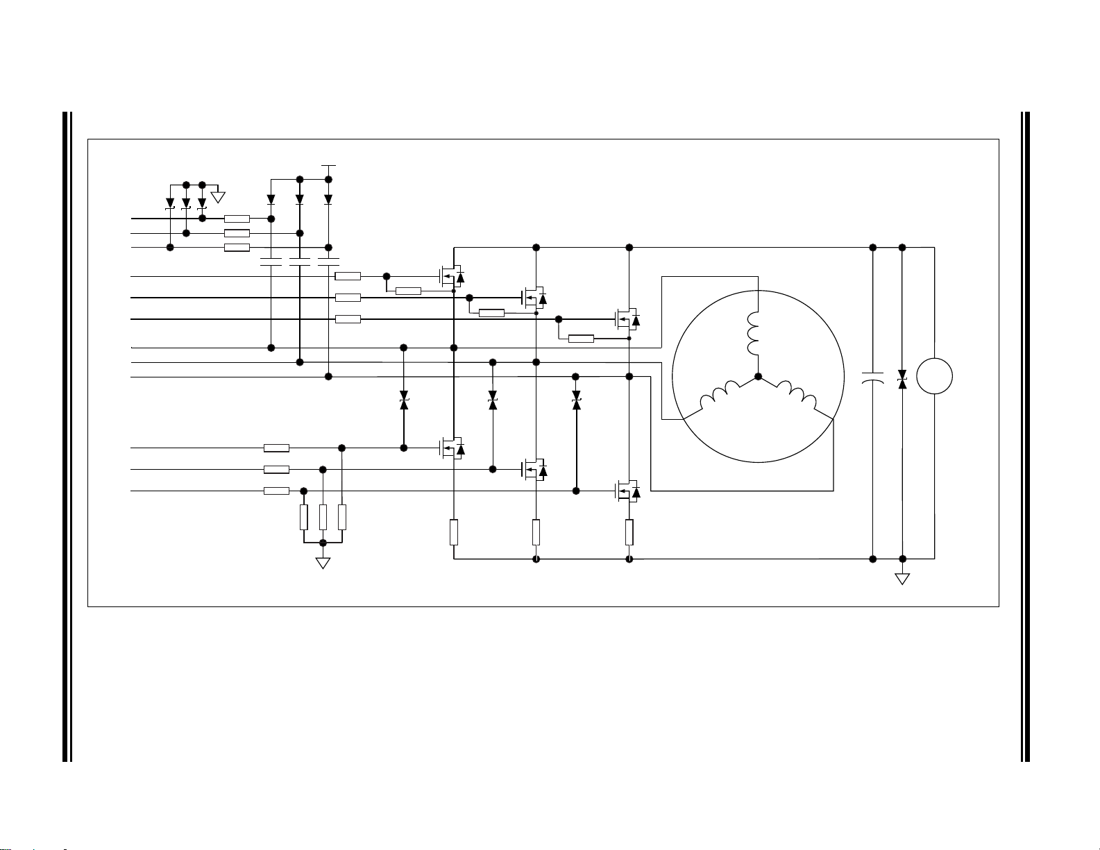
2014 Microchip Technology Inc. DS20005339A-page 55
PHA
PHB
PHC
VDD
HSA
HSB
HSC
LSA
LSB
LSC
VBA
VBB
VBC
CB
A
+
_
+12V
R
R
R
R
R
R
R
R
R
S
S
S
R
R
R
R
R
R
Figure 5-3 shows the location of the overvoltage transzorbs, gate resistors, bootstrap resistors and gate-to-source resistors.
FIGURE 5-3: Overvoltage Protection.
MCP8025/6
Page 56

MCP8025/6
NOTES:
DS20005339A-page 56 2014 Microchip Technology Inc.
Page 57

6.0 PACKAGING INFORMATION
40-Lead QFN (5x5x0.85 mm) Example
PIN 1 PIN 1
MCP8025
E/MP^^
1439256
Legend: XX...X Customer-specific information
Y Year code (last digit of calendar year)
YY Year code (last 2 digits of calendar year)
WW Week code (week of January 1 is week ‘01’)
NNN Alphanumeric traceability code
Pb-free JEDEC designator for Matte Tin (Sn)
* This package is Pb-free. The Pb-free JEDEC designator ( )
can be found on the outer packaging for this package.
Note: In the event the full Microchip part number cannot be marked on one line, it will
be carried over to the next line, thus limiting the number of available
characters for customer-specific information.
3
e
MCP8026
HPT1439
256
48-Lead TQFP (7x7x1 mm) Example
6.1 Package Marking Information
MCP8025/6
3
e
3
e
2014 Microchip Technology Inc. DS20005339A-page 57
Page 58

MCP8025/6
0.20 C
0.20 C
(DATUM B)
(DATUM A)
C
SEATING
PLANE
1
2
N
2X
TOP VIEW
SIDE VIEW
For the most current package drawings, please see the Microchip Packaging Specification located at
http://www.microchip.com/packaging
Note:
NOTE 1
1
2
N
0.10 C A B
0.10 C A B
0.08
C
Microchip Technology Drawing C04-047-002A Sheet 1 of 2
40-Lead Plastic Quad Flat, No Lead Package (MP) - 5x5 mm Body [QFN]
D2
D
E
A
B
40X b
e
0.07 C A B
0.05 C
A
(A3)
With 3.7x3.7 mm Exposed Pad
E2
A1
0.10 C
K
L
2X
DS20005339A-page 58 2014 Microchip Technology Inc.
Page 59
Microchip Technology Drawing C04-047-002A Sheet 2 of 2
For the most current package drawings, please see the Microchip Packaging Specification located at
http://www.microchip.com/packaging
Note:
Number of Terminals
Overall Height
Terminal Width
Overall Width
Overall Length
Terminal Length
Exposed Pad Width
Exposed Pad Length
Terminal Thickness
Pitch
Standoff
Units
Dimension Limits
A1
A
b
D
E2
D2
A3
e
L
E
N
0.40 BSC
0.20 REF
0.30
0.15
0.80
0.00
0.20
5.00 BSC
0.40
3.70 BSC
3.70 BSC
0.85
0.02
5.00 BSC
MILLIMETERS
MIN
NOM
40
0.50
0.25
0.90
0.05
MAX
K-0.20 -
REF: Reference Dimension, usually without tolerance, for information purposes only.
BSC: Basic Dimension. Theoretically exact value shown without tolerances.
1.
2.
3.
Notes:
Pin 1 visual index feature may vary, but must be located within the hatched area.
Package is saw singulated
Dimensioning and tolerancing per ASME Y14.5M
Terminal-to-Exposed-Pad
40-Lead Plastic Quad Flat, No Lead Package (MP) - 5x5 mm Body [QFN]
With 3.7x3.7 mm Exposed Pad
MCP8025/6
2014 Microchip Technology Inc. DS20005339A-page 59
Page 60
MCP8025/6
RECOMMENDED LAND PATTERN
For the most current package drawings, please see the Microchip Packaging Specification located at
http://www.microchip.com/packaging
Note:
SILK SCREEN
Dimension Limits
Units
C1
Optional Center Pad Width
Contact Pad Spacing
Optional Center Pad Length
Contact Pitch
Y2
X2
3.80
3.80
MILLIMETERS
0.40 BSC
MIN
E
MAX
5.00
Contact Pad Length (X40)
Contact Pad Width (X40)
Y1
X1
0.80
0.20
BSC: Basic Dimension. Theoretically exact value shown without tolerances.
Notes:
1. Dimensioning and tolerancing per ASME Y14.5M
Microchip Technology Drawing C04-2047-002A
NOM
40-Lead Plastic Quad Flat, No Lead Package (MP) - 5x5 mm Body [QFN]
With 3.7x3.7 mm Exposed Pad
E
C1
C2
Y2
X2
Y1
X1
C2Contact Pad Spacing 5.00
DS20005339A-page 60 2014 Microchip Technology Inc.
Page 61

C
SEATING
PLANE
For the most current package drawings, please see the Microchip Packaging Specification located at
http://www.microchip.com/packaging
Note:
NOTE 1
Microchip Technology Drawing C04-183A Sheet 1 of 2
48-Lead Thin Quad Flatpack (PT) - 7x7x1.0 mm Body [TQFP] With Exposed Pad
TOP VIEW
EE1
D
0.20
H A-B D
4X
D1/2
12
A
B
AA
D
D1
A1
A
H
0.10
C
0.08
C
SIDE VIEW
D2
E2
N
12
N
0.20 C A-B D
48X TIPS
0.20
H A-B D
4X
0.20
4X
E1/4
D1/4
A2
TOP VIEW
E1/2
e 48x b
0.08 C A-B D
e/2
MCP8025/6
2014 Microchip Technology Inc. DS20005339A-page 61
Page 62

MCP8025/6
Microchip Technology Drawing C04-183A Sheet 2 of 2
For the most current package drawings, please see the Microchip Packaging Specification located at
http://www.microchip.com/packaging
Note:
48-Lead Thin Quad Flatpack (PT) - 7x7x1.0 mm Body [TQFP] With Exposed Pad
H
L
(L1)
T
c
D
E
SECTION A-A
2.
1.
4.
BSC: Basic Dimension. Theoretically exact value shown without tolerances.
REF: Reference Dimension, usually without tolerance, for information purposes only.
3.
protrusions shall not exceed 0.25mm per side.
Mold Draft Angle Bottom
Molded Package Thickness
Dimension Limits
Mold Draft Angle Top
Notes:
Foot Length
Lead Width
Lead Thickness
Molded Package Length
Molded Package Width
Overall Length
Overall Width
Foot Angle
Footprint
Standoff
Overall Height
Lead Pitch
Number of Leads
12°
E
11° 13°
0.750.600.45L
12°
0.22
7.00 BSC
7.00 BSC
9.00 BSC
9.00 BSC
3.5°
1.00 REF
c
D
b
D1
E1
0.09
0.17
11°
D
E
I
L1
0°
13°
0.27
0.16-
7°
1.00
0.50 BSC
48
NOM
MILLIMETERS
A1
A2
A
e
0.05
0.95
-
Units
N
MIN
1.05
0.15
1.20
-
-
MAX
Chamfers at corners are optional; size may vary.
Pin 1 visual index feature may vary, but must be located within the hatched area.
Dimensioning and tolerancing per ASME Y14.5M
Dimensions D1 and E1 do not include mold flash or protrusions. Mold flash or
Exposed Pad Length
Exposed Pad Width
D2
E2 3.50 BSC
3.50 BSC
DS20005339A-page 62 2014 Microchip Technology Inc.
Page 63
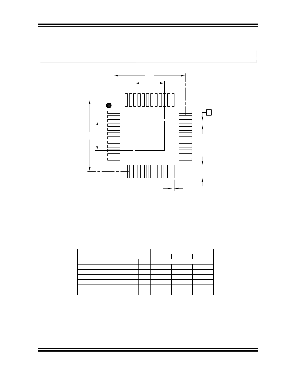
RECOMMENDED LAND PATTERN
For the most current package drawings, please see the Microchip Packaging Specification located at
http://www.microchip.com/packaging
Note:
C2
Y2
X1
C1
X2
E
Y1
Dimension Limits
Units
C1
Optional Center Tab Width
Contact Pad Spacing
Contact Pad Spacing
Optional Center Tab Length
Contact Pitch
C2
Y2
X2
3.50
3.50
MILLIMETERS
0.50 BSC
MIN
E
MAX
8.40
8.40
Contact Pad Length (X48)
Contact Pad Width (X48)
Y1
X1
1.50
0.30
BSC: Basic Dimension. Theoretically exact value shown without tolerances.
Notes:
1. Dimensioning and tolerancing per ASME Y14.5M
Microchip Technology Drawing No. C04-2183A
NOM
48-Lead Thin Quad Flatpack (PT) - 7x7x1.0 mm Body [TQFP] With Thermal Tab
MCP8025/6
2014 Microchip Technology Inc. DS20005339A-page 63
Page 64

MCP8025/6
NOTES:
DS20005339A-page 64 2014 Microchip Technology Inc.
Page 65

APPENDIX A: RE VISION HISTORY
Revision A (September 2014)
• Original Release of this Document.
MCP8025/6
2014 Microchip Technology Inc. DS20005339A-page 65
Page 66

MCP8025/6
NOTES:
DS20005339A-page 66 2014 Microchip Technology Inc.
Page 67

PRODUCT IDENTIFICATION SYSTEM
Device: MCP8025: 3-Phase Brushless DC (BLDC) Motor
Gate Driver with Power Module and LIN
MCP8025T: 3-Phase Brushless DC (BLDC) Motor
Gate Driver with Power Module and LIN
(Tape and Reel)
MCP8026: 3-Phase Brushless DC (BLDC) Motor
Gate Driver with Power Module
MCP8026T: 3-Phase Brushless DC (BLDC) Motor
Gate Driver with Power Module (Tape
and Reel)
Temperature
Warning:
115 = 115°C
Temperature
Range:
E = -40°C to +125°C (Extended)
H = -40°C to +150°C (High)
Package: MP = Plastic Quad Flat, No Lead Package – 5x5 mm
Body with 3.5x3.5 mm Exposed Pad, 40-lead
PT = Thin Quad Flatpack – 7x7x1.0 mm Body with
Exposed Pad, 48-lead
Examples:
a) MCP8025-115E/MP: Extended temperature,
40LD 5x5 QFN package
b) MCP8025T-115E/MP: Tape and Reel,
Extended temperature,
40LD 5x5 QFN package
c) MCP8025-115H/MP: High temperature,
40LD 5x5 QFN package
d) MCP8025T-115H/MP: Tape and Reel,
High temperature,
40LD 5x5 QFN package
e) MCP8026-115E/MP: Extended temperature,
40LD 5x5 QFN package
f) MCP8026T-115E/MP: Tape and Reel,
Extended temperature,
40LD 5x5 QFN package
g) MCP8026-115H/MP: High temperature,
40LD 5x5 QFN package
h) MCP8026T-115H/MP: Tape and Reel,
High temperature,
40LD 5x5 QFN package
i) MCP8025-115E/PT: Extended temperature,
48LD TQFP-EP package
j) MCP8025T-115E/PT: Tape and Reel,
Extended temperature,
48LD TQFP-EP package
k) MCP8025-115H/PT: High temperature,
48LD TQFP-EP package
l) MCP8025T-115H/PT: Tape and Reel,
High Temperature,
48LD TQFP-EP package
m) MCP8026-115E/PT: Extended temperature,
48LD TQFP-EP package
n) MCP8026T-115E/PT: Tape and Reel,
Extended temperature,
48LD TQFP-EP package
o) MCP8026-115H/PT: High temperature,
48LD TQFP-EP package
p) MCP8026T-115H/PT: Tape and Reel,
High temperature,
48LD TQFP-EP package
PART NO. -X /XX
PackageTemperature
Device
X
Temperature
Range
Warning
Note 1: Tape and Reel identifier only appears in the
catalog part number description. This identifier is used for ordering purposes and is not
printed on the device package. Check with
your Microchip Sales Office for package
availability with the Tape and Reel option.
To order or obtain information, e.g., on pricing or delivery, refer to the factory or the listed sales office.
MCP8025/6
2014 Microchip Technology Inc. DS20005339A-page 67
Page 68

MCP8025/6
NOTES:
DS20005339A-page 68 2014 Microchip Technology Inc.
Page 69

Note the following details of the code protection feature on Microchip devices:
YSTEM
CERTIFIED BY DNV
== ISO/TS 16949 ==
• Microchip products meet the specification contained in their particular Microchip Data Sheet.
• Microchip believes that its family of products is one of the most secure families of its kind on the market today, when used in the
intended manner and under normal conditions.
• There are dishonest and possibly illegal methods used to breach the code protection feature. All of these methods, to our
knowledge, require using the Microchip products in a manner outside the operating specifications contained in Microchip’s Data
Sheets. Most likely, the person doing so is engaged in theft of intellectual property.
• Microchip is willing to work with the customer who is concerned about the integrity of their code.
• Neither Microchip nor any other semiconductor manufacturer can guarantee the security of their code. Code protection does not
mean that we are guaranteeing the product as “unbreakable.”
Code protection is constantly evolving. We at Microchip are committed to continuously improving the code protection features of our
products. Attempts to break Microchip’s code protection feature may be a violation of the Digital Millennium Copyright Act. If such acts
allow unauthorized access to your software or other copyrighted work, you may have a right to sue for relief under that Act.
Information contained in this publication regarding device
applications and the like is provided only for your convenience
and may be superseded by updates. It is your responsibility to
ensure that your application meets with your specifications.
MICROCHIP MAKES NO REPRESENTATIONS OR
WARRANTIES OF ANY KIND WHETHER EXPRESS OR
IMPLIED, WRITTEN OR ORAL, STATUTORY OR
OTHERWISE, RELATED TO THE INFORMATION,
INCLUDING BUT NOT LIMITED TO ITS CONDITION,
QUALITY, PERFORMANCE, MERCHANTABILITY OR
FITNESS FOR PURPOSE
. Microchip disclaims all liability
arising from this information and its use. Use of Microchip
devices in life support and/or safety applications is entirely at
the buyer’s risk, and the buyer agrees to defend, indemnify and
hold harmless Microchip from any and all damages, claims,
suits, or expenses resulting from such use. No licenses are
conveyed, implicitly or otherwise, under any Microchip
intellectual property rights.
Trademarks
The Microchip name and logo, the Microchip logo, dsPIC,
FlashFlex, flexPWR, JukeBlox, K
LANCheck, MediaLB, MOST, MOST logo, MPLAB,
OptoLyzer, PIC, PICSTART, PIC
EELOQ, KEELOQ logo, Kleer,
32
logo, RightTouch, SpyNIC,
SST, SST Logo, SuperFlash and UNI/O are registered
trademarks of Microchip Technology Incorporated in the
U.S.A. and other countries.
The Embedded Control Solutions Company and mTouch are
registered trademarks of Microchip Technology Incorporated
in the U.S.A.
Analog-for-the-Digital Age, BodyCom, chipKIT, chipKIT logo,
CodeGuard, dsPICDEM, dsPICDEM.net, ECAN, In-Circuit
Serial Programming, ICSP, Inter-Chip Connectivity, KleerNet,
KleerNet logo, MiWi, MPASM, MPF, MPLAB Certified logo,
MPLIB, MPLINK, MultiTRAK, NetDetach, Omniscient Code
Generation, PICDEM, PICDEM.net, PICkit, PICtail,
RightTouch logo, REAL ICE, SQI, Serial Quad I/O, Total
Endurance, TSHARC, USBCheck, VariSense, ViewSpan,
WiperLock, Wireless DNA, and ZENA are trademarks of
Microchip Technology Incorporated in the U.S.A. and other
countries.
SQTP is a service mark of Microchip Technology Incorporated
in the U.S.A.
Silicon Storage Technology is a registered trademark of
Microchip Technology Inc. in other countries.
GestIC is a registered trademarks of Microchip Technology
Germany II GmbH & Co. KG, a subsidiary of Microchip
Technology Inc., in other countries.
All other trademarks mentioned herein are property of their
respective companies.
© 2014, Microchip Technology Incorporated, Printed in the
U.S.A., All Rights Reserved.
ISBN: 978-1-63276-623-6
QUALITY MANAGEMENT S
2014 Microchip Technology Inc. DS20005339A-page 69
Microchip received ISO/TS-16949:2009 certification for its worldwide
headquarters, design and wafer fabrication facilities in Chandler and
Tempe, Arizona; Gresham, Oregon and design centers in California
and India. The Company’s quality system processes and procedures
are for its PIC
devices, Serial EEPROMs, microperipherals, nonvolatile memory and
analog products. In addition, Microchip’s quality system for the design
and manufacture of development systems is ISO 9001:2000 certified.
®
MCUs and dsPIC® DSCs, KEELOQ
®
code hopping
Page 70

Worldwide Sales and Service
AMERICAS
Corporate Office
2355 West Chandler Blvd.
Chandler, AZ 85224-6199
Tel: 480-792-7200
Fax: 480-792-7277
Technical Support:
http://www.microchip.com/
support
Web Address:
www.microchip.com
Atlanta
Duluth, GA
Tel: 678-957-9614
Fax: 678-957-1455
Austin, TX
Tel: 512-257-3370
Boston
Westborough, MA
Tel: 774-760-0087
Fax: 774-760-0088
Chicago
Itasca, IL
Tel: 630-285-0071
Fax: 630-285-0075
Cleveland
Independence, OH
Tel: 216-447-0464
Fax: 216-447-0643
Dallas
Addison, TX
Tel: 972-818-7423
Fax: 972-818-2924
Detroit
Novi, MI
Tel: 248-848-4000
Houston, TX
Tel: 281-894-5983
Indianapolis
Noblesville, IN
Tel: 317-773-8323
Fax: 317-773-5453
Los Angeles
Mission Viejo, CA
Tel: 949-462-9523
Fax: 949-462-9608
New Yor k , NY
Tel: 631-435-6000
San Jose, CA
Tel: 408-735-9110
Canada - Toronto
Tel: 905-673-0699
Fax: 905-673-6509
ASIA/PACIFIC
Asia Pacific Office
Suites 3707-14, 37th Floor
Tower 6, The Gateway
Harbour City, Kowloon
Hong Kong
Tel: 852-2943-5100
Fax: 852-2401-3431
Australia - Sydney
Tel: 61-2-9868-6733
Fax: 61-2-9868-6755
China - Beijing
Tel: 86-10-8569-7000
Fax: 86-10-8528-2104
China - Chengdu
Tel: 86-28-8665-5511
Fax: 86-28-8665-7889
China - Chongqing
Tel: 86-23-8980-9588
Fax: 86-23-8980-9500
China - Hangzhou
Tel: 86-571-8792-8115
Fax: 86-571-8792-8116
China - Hong Kong SAR
Tel: 852-2943-5100
Fax: 852-2401-3431
China - Nanjing
Tel: 86-25-8473-2460
Fax: 86-25-8473-2470
China - Qingdao
Tel: 86-532-8502-7355
Fax: 86-532-8502-7205
China - Shanghai
Tel: 86-21-5407-5533
Fax: 86-21-5407-5066
China - Shenyang
Tel: 86-24-2334-2829
Fax: 86-24-2334-2393
China - Shenzhen
Tel: 86-755-8864-2200
Fax: 86-755-8203-1760
China - Wuhan
Tel: 86-27-5980-5300
Fax: 86-27-5980-5118
China - Xian
Tel: 86-29-8833-7252
Fax: 86-29-8833-7256
China - Xiamen
Tel: 86-592-2388138
Fax: 86-592-2388130
China - Zhuhai
Tel: 86-756-3210040
Fax: 86-756-3210049
ASIA/PACIFIC
India - Bangalore
Tel: 91-80-3090-4444
Fax: 91-80-3090-4123
India - New Delhi
Tel: 91-11-4160-8631
Fax: 91-11-4160-8632
India - Pune
Tel: 91-20-3019-1500
Japan - Osaka
Tel: 81-6-6152-7160
Fax: 81-6-6152-9310
Japan - Tokyo
Tel: 81-3-6880- 3770
Fax: 81-3-6880-3771
Korea - Daegu
Tel: 82-53-744-4301
Fax: 82-53-744-4302
Korea - Seoul
Tel: 82-2-554-7200
Fax: 82-2-558-5932 or
82-2-558-5934
Malaysia - Kuala Lumpur
Tel: 60-3-6201-9857
Fax: 60-3-6201-9859
Malaysia - Penang
Tel: 60-4-227-8870
Fax: 60-4-227-4068
Philippines - Manila
Tel: 63-2-634-9065
Fax: 63-2-634-9069
Singapore
Tel: 65-6334-8870
Fax: 65-6334-8850
Tai wan - Hsin Chu
Tel: 886-3-5778-366
Fax: 886-3-5770-955
Taiwan - Kaohsiung
Tel: 886-7-213-7830
Taiwan - Taipei
Tel: 886-2-2508-8600
Fax: 886-2-2508-0102
Thailand - Bangkok
Tel: 66-2-694-1351
Fax: 66-2-694-1350
EUROPE
Austria - Wels
Tel: 43-7242-2244-39
Fax: 43-7242-2244-393
Denmark - Copenhagen
Tel: 45-4450-2828
Fax: 45-4485-2829
France - Paris
Tel: 33-1-69-53-63-20
Fax: 33-1-69-30-90-79
Germany - Dusseldorf
Tel: 49-2129-3766400
Germany - Munich
Tel: 49-89-627-144-0
Fax: 49-89-627-144-44
Germany - Pforzheim
Tel: 49-7231-424750
Italy - Milan
Tel: 39-0331-742611
Fax: 39-0331-466781
Italy - Venice
Tel: 39-049-7625286
Netherlands - Drunen
Tel: 31-416-690399
Fax: 31-416-690340
Poland - Wars a w
Tel: 48-22-3325737
Spain - Madrid
Tel: 34-91-708-08-90
Fax: 34-91-708-08-91
Sweden - Stockholm
Tel: 46-8-5090-4654
UK - Wokingham
Tel: 44-118-921-5800
Fax: 44-118-921-5820
03/25/14
DS20005339A-page 70 2014 Microchip Technology Inc.
 Loading...