

Page 1

MCP6V51
VIN+
V
SS
VIN–
1
2
3
5
4
V
DD
V
OUT
MCP6V51
SOT-23-5
VIN+
VIN–
V
SS
1
2
3
4
8
7
6
5
NC
NC
V
DD
V
OUT
NC
MCP6V51
MSOP-8
R
F
8.2 nF
V
OUT
40V
DD
R
SHUNT
R
G
0.05
20 k
100
U
1
MCP6V51
+
-
40V
DD
C
F
Load
I
L
45V, 2 MHz Zero-Drift Op Amp with EMI Filtering
Features
• High DC Precision:
-V
Drift: 36 nV/°C (max.)
OS
-VOS: 15 µV (max.)
- Open-Loop Gain: 140 dB (min.)
- PSRR: 134 dB (min.)
- CMRR: 135 dB (min.)
•Low Noise:
- 10.2 nV/ Hz at 1 kHz
-E
: 0.21 µV
ni
•Low Power:
-I
: 470 µA/amplifier (typ.)
Q
- Wide Supply Voltage Range: 4.5V to 45V
•Easy to Use:
- Input Range incl. Negative Rail
- Rail-to-Rail Output
- EMI Filtered Inputs
- Gain Bandwidth Product: 2 MHz
- Slew Rate 1.2V/µs
- Unity Gain Stable
• Small Packages: 5-Lead SOT23, 8-Lead MSOP
• Extended Temperature Range: -40°C to +125°C
, f = 0.1 Hz to 10 Hz
P-P
General Description
The Microchip Technology Inc. MCP6V51 operational
amplifier employs dynamic offset correction for very
low offset and offset drift. The device has a gain
bandwidth product of 2 MHz (typical). It is unity-gain
stable, has virtually no 1/f noise and excellent Power
Supply Rejection Ratio (PSRR) and Common Mode
Rejection Ratio (CMRR). The product operates with a
single supply voltage that can range from 4.5V to 45V,
(±2.25V to ±22.5V), while drawing 470 µA (typical) of
quiescent current.
The MCP6V51 op amp is offered as a single-channel
amplifier and is designed using an advanced CMOS
process.
Package Types
Typical Applications
• Industrial Instrumentation, PLC
• Process Control
• Power Control Loops
Typical Application Circuit
• Sensor Conditioning
• Electronic Weight Scales
• Medical Instrumentation
• Automotive Monitors
• Low-side Current Sensing
Design Aids
• Microchip Advanced Part Selector (MAPS)
• Application Notes
Related Parts
• MCP6V71/1U/2/4: Zero-Drift, 2 MHz, 1.8V to 5V
• MCP6V81/1U/2/4: Zero-Drift, 5 MHz, 1.8V to 5V
2018 Microchip Technology Inc. DS20006136A-page 1
Page 2

MCP6V51
-8
-6
-4
-2
0
2
4
6
8
-50 -25 0 25 50 75 100 125
Input Offset Voltage (μV)
Ambient Temperature (°C)
22 Samples
V
DD
= 4.5V
-8
-6
-4
-2
0
2
4
6
8
-50-250 255075100125
Input Offset Voltage (μV)
Ambient Temperature (°C)
22 Samples
V
DD
= 45V
Figure 1 and Figure 2 show input offset voltage versus
ambient temperature for different power supply
voltages.
FIGURE 1: Input Offset Voltage vs.
Ambient Temperature with V
DD
=4.5V.
As seen in Figure 1 and Figure 2, the MCP6V51 op
amps have excellent performance across temperature.
The input offset voltage temperature drift (TC
) shown
1
is well within the specified maximum values of
31 nV/°C at VDD= 4.5V and 36 nV/°C at VDD=45V.
This performance supports applications with stringent
DC precision requirements. In many cases, it will not be
necessary to correct for temperature effects (i.e.,
calibrate) in a design. In the other cases, the correction
will be small.
FIGURE 2: Input Offset Voltage vs.
Ambient Temperature with V
DS20006136A-page 2 2018 Microchip Technology Inc.
DD
= 45V.
Page 3

MCP6V51
1.0 ELECTRICAL CHARACTERISTICS
1.1 Absolute Maximum Ratings †
VDD-VSS ................................................................................................................................................................ 49.5V
Current at Input Pins ............................................................................................................................................±10 mA
Analog Inputs (V
All Other Inputs and Outputs .................................................................................................... V
Difference Input Voltage .............................................................................................................................................±1V
Output Short Circuit Current ........................................................................................................................... Continuous
Current at Output and Supply Pins ......................................................................................................................±50 mA
Storage Temperature .............................................................................................................................-65°C to +150°C
Maximum Junction Temperature .......................................................................................................................... +150°C
ESD protection on all pins (HBM, CDM, MM) 2 kV, 750V, 200V
†Notice: Stresses above those listed under “Absolute Maximum Ratings” may cause permanent damage to the
device. This is a stress rating only and functional operation of the device at those or any other conditions above those
indicated in the operational listings of this specification is not implied. Exposure to maximum rating conditions for
extended periods may affect device reliability.
Note 1: See Section 4.2.1, Input Protection.
+ and VIN-) (Note 1)..................................................................................... VSS- 1.0V to VDD+1.0V
IN
- 0.3V to VDD+0.3V
SS
1.2 Electrical Specifications
DC ELECTRICAL SPECIFICATIONS
Electrical Characteristics: Unless otherwise indicated, TA= +25°C, VDD= +4.5V to +45V, VSS= GND,
V
CM=VDD
/3, V
OUT=VDD
Parameters Sym. Min. Typ. Max. Units Conditions
Input Offset
Input Offset Voltage V
Input Offset Voltage Drift with
Temperature (Linear Temp. Co.)
Input Offset Voltage Quadratic
Te m p . C o.
Input Offset Voltage Aging V
Power Supply Rejection Ratio PSRR 134 160 — dB
Input Bias Current and Impedance
Input Bias Current I
Note 1: Not production tested. Limits set by characterization and/or simulation and provided as design guidance
only.
2: Figure 2-17 shows how V
/2, VL=VDD/2, RL=10k to VL and CL= 100 pF (refer to Figure 1-4 and Figure 1-5).
-15 ±2.4 +15 µV TA=+25°C
-31 ±5 +31 nV/°C TA= -40 to +125°C,
=4.5V (Note 1)
V
DD
-36 ±7 +36 nV/°C TA= -40 to +125°C,
= 45V
V
DD
TC
TC
OS
1
1
(Note 1)
TC
TC
OS
2
2
—±42—nV/
—±38—nV/
— ±2 — µV 408 hours Life Test at
TA= -40 to +125°C
2
°C
V
DD
TA= -40 to +125°C
2
°C
V
DD
=4.5V
= 45V
+150°C,
measured at +25°C
B
CML
124 138 — dB T
-250 ±60 +250 pA VDD= 45V
and V
changed across temperature for the first production lot.
CMH
= -40°C to +125°C
A
V
= 45V (Note 1)
DD
2018 Microchip Technology Inc. DS20006136A-page 3
Page 4

MCP6V51
DC ELECTRICAL SPECIFICATIONS (CONTINUED)
Electrical Characteristics: Unless otherwise indicated, TA= +25°C, VDD= +4.5V to +45V, VSS= GND,
V
CM=VDD
Input Bias Current across
Temperature
Input Offset Current I
Input Offset Current across
Temperature
Common Mode Input Impedance Z
Differential Input Impedance Z
Common Mode
Common Mode
Input Voltage Range Low
Common Mode
Input Voltage Range High
Common Mode Rejection Ratio CMRR 110 125 — dB V
Open-Loop Gain
DC Open-Loop Gain A
Output
Minimum Output Voltage Swing V
Note 1: Not production tested. Limits set by characterization and/or simulation and provided as design guidance
/3, V
OUT=VDD
/2, VL=VDD/2, RL=10k to VL and CL= 100 pF (refer to Figure 1-4 and Figure 1-5).
Parameters Sym. Min. Typ. Max. Units Conditions
I
B
I
B
OS
I
OS
I
OS
CM
DIFF
V
CML
V
CMHVDD
—±80—pAT
=+85°C
A
-4 ±1.4 +4 nA TA= +125°C (Note 1)
-1 ±0.28 +1 nA VDD= 45V
— ±0.32 — nA TA=+85°C
-8 ±0.45 +8 nA TA= +125°C (Note 1)
— 120G||3 — ||pF
—2.5M||5.2 —||pF
——V
-0.3 V (Note 2)
SS
-2.1 — — V (Note 2)
=4.5V,
DD
= -0.3V to 2.4V
V
CM
(Note 2)
106 116 — dB V
=4.5V
DD
= -40°C to +125°C,
T
A
(Note 1)
CMRR 135 150 — dB V
= 45V,
DD
= -0.3V to 42.9V
V
CM
(Note 2)
128 140 — dB V
= 45V
DD
= -40°C to +125°C,
T
A
(Note 1)
OL
124 142 — dB VDD=4.5V,
V
= 0.3V to 4.2V
OUT
120 139 — dB VDD=4.5V
= -40°C to +125°C,
T
A
(Note 1)
A
OL
140 164 — dB VDD= 45V,
= 0.3V to 44.7V
V
OUT
134 160 — dB V
= 45V
DD
= -40°C to +125°C,
T
A
(Note 1)
OL
—VSS+45 VSS+60 mV RL=1k, VDD = 4.5V
—V
—V
+ 500 VSS+1000 RL=1k, VDD = 45V
SS
+6 VSS+20 RL=10k, VDD = 4.5V
SS
—VSS+50 VSS+70 RL=10k, VDD = 45V
only.
2: Figure 2-17 shows how V
CML
and V
changed across temperature for the first production lot.
CMH
DS20006136A-page 4 2018 Microchip Technology Inc.
Page 5

MCP6V51
DC ELECTRICAL SPECIFICATIONS (CONTINUED)
Electrical Characteristics: Unless otherwise indicated, TA= +25°C, VDD= +4.5V to +45V, VSS= GND,
V
CM=VDD
Maximum Output Voltage Swing V
Output Short Circuit Current I
Closed-loop Output Resistance R
Capacitive Load Drive C
Power Supply
Supply Voltage V
Quiescent Current per Amplifier I
Power-on Reset (POR) Trip
Voltage
Note 1: Not production tested. Limits set by characterization and/or simulation and provided as design guidance
/3, V
OUT=VDD
/2, VL=VDD/2, RL=10k to VL and CL= 100 pF (refer to Figure 1-4 and Figure 1-5).
Parameters Sym. Min. Typ. Max. Units Conditions
VDD-150 VDD- 100 — mV RL=1k, VDD = 4.5V
OH
V
- 2500 VDD-1500 — RL=1k, VDD = 45V
DD
-20 VDD-12 — RL=10k, VDD = 4.5V
V
DD
VDD-200 VDD- 100 — RL=10k, VDD = 45V
+ —46—mA
SC
- —36—mA
I
SC
OUT
—16 — f=0.1MHz, IO=0,
G=1
L
DD
Q
—100—pFG=1
4.5 — 45 V
310 460 590 µA VDD= 4.5V, IO=0
310 470 590 µA VDD= 45V, IO=0
— 540 670 µA IO=0,
T
= -40 to +125°C
A
(Note 1)
(Figure 2-22)
V
POR
—2.3—V
only.
2: Figure 2-17 shows how V
CML
and V
changed across temperature for the first production lot.
CMH
AC ELECTRICAL SPECIFICATIONS
Electrical Characteristics: Unless otherwise indicated, TA= +25°C, VDD= +4.5V to +45V, VSS= GND,
V
CM=VDD
/3, V
OUT=VDD
Parameters Sym. Min. Typ. Max. Units Conditions
Amplifier AC Response
Gain Bandwidth Product GBWP — 1.8 — MHz V
Slew Rate SR — 1.2 — V/µs (Figure 2-44)
Phase Margin PM — 66 — deg. V
Amplifier Noise Response
Input Noise Voltage E
Input Noise Voltage Density e
Input Noise Current Density i
Amplifier Step Response
Start-Up Time t
Offset Correction Settling Time t
Note 1: Behavior may vary with different gains; see Section 4.3.3 “Offset at Power-Up”.
2: t
STL
and t
/2, VL=VDD/2, RL=10k to VL and CL= 100 pF (refer to Figure 1-4 and Figure 1-5).
= 4.5V, VIN= 10 mVpp, Gain = 100
DD
—2—MHzV
—0.1—µV
ni
E
ni
STR
STL
include some uncertainty due to clock edge timing.
ODR
—0.21—µV
ni
—10.2—nV/Hz f = 1 kHz
ni
—4—fA/Hz
— 200 — µs G = +1, 1% V
—45— µsG=+1, VIN step of 2V,
P-P
P-P
= 45V, VIN=10mVpp, Gain=100
DD
= 45V
DD
f=0.01Hz to 1Hz
f = 0.1 Hz to 10 Hz
settling (Note 1)
OUT
within ±100 µV of its final value
V
OS
2018 Microchip Technology Inc. DS20006136A-page 5
Page 6

MCP6V51
AC ELECTRICAL SPECIFICATIONS (CONTINUED)
Electrical Characteristics: Unless otherwise indicated, TA= +25°C, VDD= +4.5V to +45V, VSS= GND,
V
CM=VDD
Output Overdrive Recovery Time t
EMI Protection
EMI Rejection Ratio EMIRR — 80 — dB V
Note 1: Behavior may vary with different gains; see Section 4.3.3 “Offset at Power-Up”.
TEMPERATURE SPECIFICATIONS
Electrical Characteristics: Unless otherwise indicated, all limits are specified for: VDD= +4.5V to +45V, VSS= GND.
Temperature Ranges
Specified Temperature Range T
Operating Temperature Range T
Storage Temperature Range T
Thermal Package Resistances
Thermal Resistance, 8LD-MSOP
Thermal Resistance, 5LD-SOT-23
Note 1: Operation must not cause T
/3, V
OUT=VDD
/2, VL=VDD/2, RL=10k to VL and CL= 100 pF (refer to Figure 1-4 and Figure 1-5).
Parameters Sym. Min. Typ. Max. Units Conditions
ODR
— 65 — µs G = -10, ±0.5V input overdrive to VDD/2,
50% point to V
V
IN
=0.1VPK, f = 400 MHz, VDD= 45V
IN
—95— VIN=0.1VPK, f = 900 MHz, VDD= 45V
—108— V
=0.1VPK, f = 1800 MHz, VDD=45V
IN
—109— VIN=0.1VPK, f = 2400 MHz, VDD=45V
—109— VIN=0.1VPK, f = 5600 MHz, VDD=45V
2: t
STL
and t
include some uncertainty due to clock edge timing.
ODR
Parameters Sym. Min. Typ. Max. Units Conditions
A
A
A
JA
JA
to exceed Maximum Junction Temperature specification (+150°C).
J
-40 — +125 °C
-40 — +125 °C (Note 1)
-65 — +150 °C
—206 — °C/W
—115 — °C/W
90% point (Note 2)
OUT
DS20006136A-page 6 2018 Microchip Technology Inc.
Page 7

MCP6V51
V
DD
V
OUT
1.01(VDD/3)
0.99(V
DD
/3)
t
STR
0V
V
DD
2.3V
V
IN
V
OS
VOS+100µV
VOS–100µV
t
STL
V
IN
V
OUT
V
DD
V
SS
t
ODR
t
ODR
VDD/2
V
DD
R
G
R
F
R
N
V
OUT
V
IN
VDD/3
1µF
C
L
R
L
V
L
100 nF
R
ISO
MCP6V51
+
-
V
DD
R
G
R
F
R
N
V
OUT
VDD/3
V
IN
1µF
C
L
R
L
V
L
100 nF
R
ISO
MCP6V51
+
-
V
DD
V
OUT
1µF
C
L
V
L
R
ISO
1.1 k
249
1.1 k 500
V
IN
V
REF=VDD
/3
0.1%
0.1% 25 turn
10 k
10 k
0.1%
0.1%
R
L
0
100 pF open
100 nF
1%
MCP6V51
1.3 Timing Diagrams
The Timing Diagrams provide a depiction of the
Amplifier Step Response specifications listed under the
AC Electrical Specifications table.
FIGURE 1-1: Amplifier Start-Up.
FIGURE 1-2: Offset Correction Settling
Time.
1.4 Test Circuits
The circuits used for most DC and AC tests are shown
in Figure 1-4 and Figure 1-5. Lay the bypass
capacitors out as discussed in Section 4.3.10 “Supply
Bypassing and Filtering”. R
combination of R
and RG to minimize bias current
F
effects.
FIGURE 1-4: AC and DC Test Circuit for Most Noninverting Gain Conditions.
is equal to the parallel
N
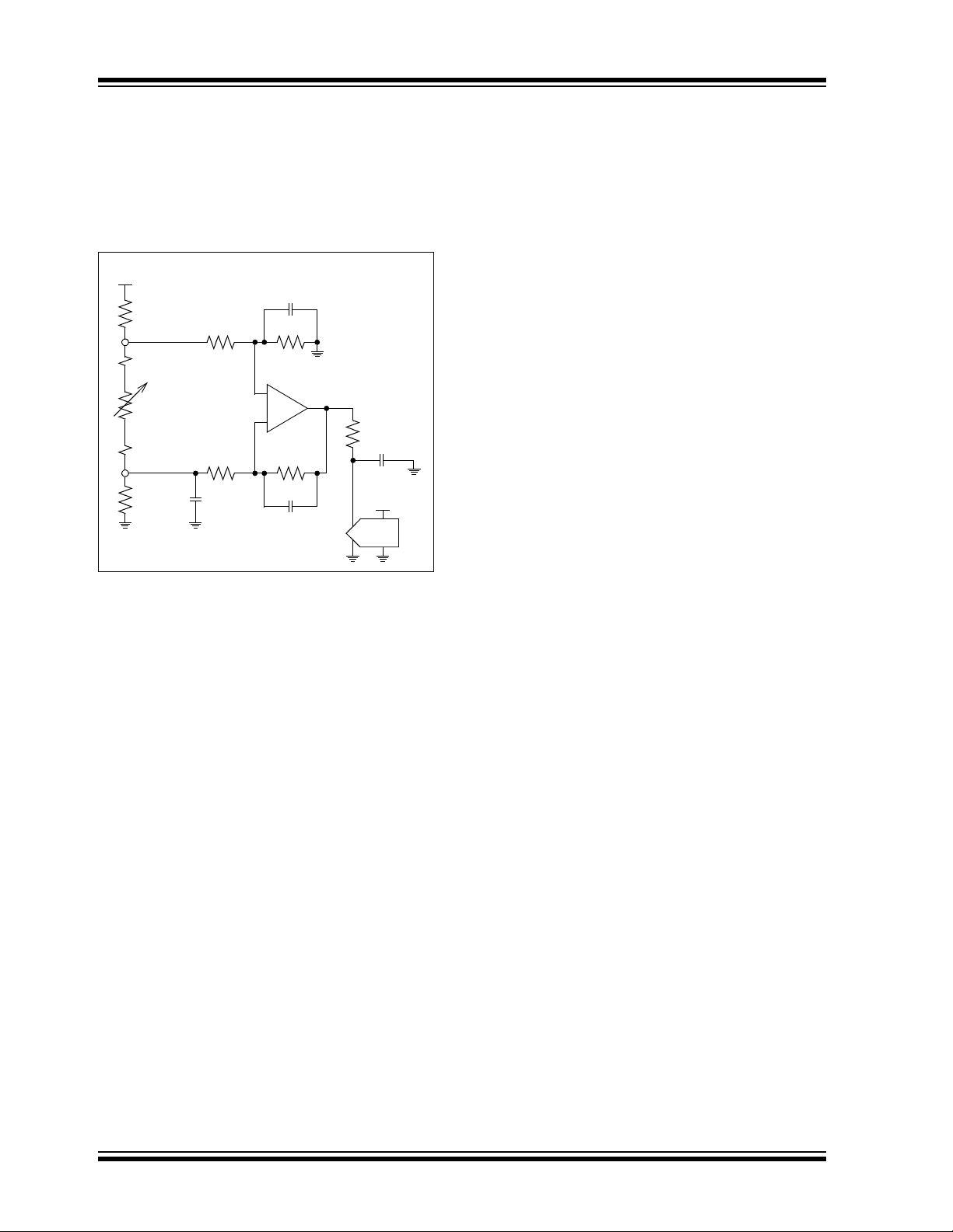
FIGURE 1-5: AC and DC Test Circuit for Most Inverting Gain Conditions.
The circuit in Figure 1-6 tests the input’s dynamic
behavior (i.e., t
balances the resistor network (V
FIGURE 1-3: Output Overdrive Recovery.
at DC). The op amp’s Common Mode Input Voltage is
V
CM=VIN
V
OUT
/3. The error at the input (V
with a noise gain of approx. 10 V/V.
2018 Microchip Technology Inc. DS20006136A-page 7
FIGURE 1-6: Test Circuit for Dynamic Input Behavior.
STR
, t
STL
and t
). The potentiometer
ODR
should equal V
OUT
) appears at
ERR
REF
Page 8

MCP6V51
NOTES:
DS20006136A-page 8 2018 Microchip Technology Inc.
Page 9

MCP6V51
0%
5%
10%
15%
20%
25%
30%
35%
-10-8-6-4-20246810
Percentage of Occurences
Input Offset Voltage (μV)
7611 Samples
TA= 25ºC
VDD= 4.5V
VDD= 45V
0%
5%
10%
15%
20%
25%
30%
35%
40%
-18-15-12-9-6-30369121518
Percentage of Occurances
Input Offset Voltage Drift; TC1(nV/°C)
22 Samples
T
A
= -40°C to +125°C
VDD= 4.5V
VDD= 45V
-20
-15
-10
-5
0
5
10
15
20
0 5 10 15 20 25 30 35 40 45
Input Offset Voltage (μV)
Power Supply Voltage (V)
TA= +85°C
T
A
= +125°C
TA= +25°C
TA= -40°C
-8
-6
-4
-2
0
2
4
6
8
0.0 0.5 1.0 1.5 2.0 2.5 3.0 3.5 4.0 4.5
Input Offset Voltage (μV)
Output Voltage (V)
Representative Part
VDD= 4.5V
TA= +125°C
T
A
= +85°C
T
A
= +25°C
T
A
= - 40°C
-8
-6
-4
-2
0
2
4
6
8
-1 4 9 14 19 24 29 34 39 44
Input Offset Voltage (μV)
Output Voltage (V)
Representative Part
VDD= 45V
TA= +125°C
T
A
= +85°C
T
A
= +25°C
T
A
= - 40°C
-8.0
-6.0
-4.0
-2.0
0.0
2.0
4.0
6.0
8.0
-0.3 0.0 0.3 0.6 0.9 1.2 1.5 1.8 2.1 2.4
Input Offset Voltage (μV)
Common Mode Input Voltage (V)
TA= +125°C
TA= +85°C
TA= +25°C
TA= - 40°C
VDD= 4.5V
Representative Part
2.0 TYPICAL PERFORMANCE CURVES
Note: The graphs and tables provided following this note are a statistical summary based on a limited number of
samples and are provided for informational purposes only. The performance characteristics listed herein
are not tested or guaranteed. In some graphs or tables, the data presented may be outside the specified
operating range (e.g., outside specified power supply range) and therefore outside the warranted range.
Note: Unless otherwise indicated, TA=+25°C, VDD= +4.5V to +45V, VSS= GND, VCM=VDD/3, V
V
L=VDD
/2, RL=10k to VL and CL= 100 pF.
2.1 DC Input Precision
FIGURE 2-1: Input Offset Voltage.
FIGURE 2-4: Input Offset Voltage vs.
Output Voltage with V
DD
=4.5V.
OUT=VDD
/2,
FIGURE 2-2: Input Offset Voltage Drift.
FIGURE 2-3: Input Offset Voltage vs.
Power Supply Voltage.
2018 Microchip Technology Inc. DS20006136A-page 9
FIGURE 2-5: Input Offset Voltage vs.
Output Voltage with V
DD
=45V.
FIGURE 2-6: Input Offset Voltage vs.
Common Mode Voltage with V
DD
=4.5V
Page 10

MCP6V51
-8.0
-6.0
-4.0
-2.0
0.0
2.0
4.0
6.0
8.0
-1 4 9 14 19 24 29 34 39 44
Input Offset Voltage (μV)
Common Mode Input Voltage (V)
TA= +125°C
T
A
= +85°C
T
A
= +25°C
T
A
= - 40°C
VDD= 45V
Representative Part
0%
10%
20%
30%
40%
50%
60%
70%
80%
90%
-1
-0.8
-0.6
-0.4
-0.2
0
0.2
0.4
0.6
0.8
1
Percentage of Occurrences
1/CMRR (μV/V)
488 Samples
TA= +25ºC
VDD= 4.5V
VDD= 45V
0%
5%
10%
15%
20%
25%
30%
35%
-0.1
-0.08
-0.06
-0.04
-0.02
0
0.02
0.04
0.06
0.08
0.1
Percentage of Occurrences
1/PSRR (μV/V)
488 Samples
TA= +25ºC
0%
10%
20%
30%
40%
50%
60%
-0.5
-0.4
-0.3
-0.2
-0.1
0
0.1
0.2
0.3
0.4
0.5
Percentage of Occurrences
1/AOL(μV/V)
474 Samples
TA= +25ºC
VDD= 45V
VDD= 4.5V
110
120
130
140
150
160
-50-250 255075100125
CMRR, PSRR (dB)
Ambient Temperature (°C)
PSRR
CMRR @ VDD= 45V
@ V
DD
= 4.5V
120
130
140
150
160
170
-50 -25 0 25 50 75 100 125
DC Open-Loop Gain (dB)
Ambient Temperature (°C)
VDD= 4.5V
VDD= 45V
FIGURE 2-7: Input Offset Voltage vs.
Common Mode Voltage with V
DD
= 45V.
FIGURE 2-8: CMRR.
FIGURE 2-10: DC Open-Loop Gain.
FIGURE 2-11: CMRR and PSRR vs.
Ambient Temperature.
FIGURE 2-9: PSRR.
DS20006136A-page 10 2018 Microchip Technology Inc.
FIGURE 2-12: DC Open-Loop Gain vs. Ambient Temperature.
Page 11

MCP6V51
-500
-400
-300
-200
-100
0
100
200
300
400
500
Input Bias, Offset Currents (pA)
Input Common Mode Voltage (V)
Input Bias Current
Input Offset Current
VDD= 45V
TA= +85 ºC
0 5 10 15 20 25 30 35 40 45
-1000
-500
0
500
1000
1500
2000
Input Bias, Offset Currents (pA)
Input Common Mode Voltage (V)
Input Bias Current
Input Offset Current
VDD= 45V
TA= +125 ºC
0 5 10 15 20 25 30 35 40 45
25
35
45
55
65
75
85
95
105
115
125
Input Bias, Offset Currents (A)
Ambient Temperature (°C)
10n
100
p
10
p
1
p
1n
I
B
I
OS
4.5V
45V
-1.0 -0.9 -0.8 -0.7 -0.6 -0.5 -0.4 -0.3 -0.2 -0.1 0.0
Input Current Magnitude (A)
Input Voltage (V)
1m
10μ
100n
10n
1n
TA= +125°C
T
A
= +85°C
T
A
= +25°C
T
A
= -40°C
100μ
1μ
100p
FIGURE 2-13: Input Bias and Offset
Currents vs. Common Mode Input Voltage with
T
= +85°C.
A
FIGURE 2-14: Input Bias and Offset
Currents vs. Common Mode Input Voltage with
T
= +125°C.
A
FIGURE 2-16: Input Bias Current vs. Input
Voltage (Below V
SS
).
FIGURE 2-15: Input Bias and Offset
Currents vs. Ambient Temperature with
= 45V.
V
DD
2018 Microchip Technology Inc. DS20006136A-page 11
Page 12

MCP6V51
-0.5
0
0.5
1
1.5
2
2.5
-50 -25 0 25 50 75 100 125
Input Common Mode Voltage
Headroom (V)
Ambient Temperature (°C)
Upper (VDD-V
CMH
)
Lower (V
CML-VSS
)
1
10
100
1000
0.1 1 10
Output Voltage Headroom
(mV)
Output Current Magnitude (mA)
VDD= 45V
VDD= 4.5V
VDD-V
OH
VOL-V
SS
0
500
1000
1500
2000
-50 -25 0 25 50 75 100 125
Output Voltage Headroom (mV)
Ambient Temperature (°C)
VDD-V
OH
VDD= 45V
VOL-V
SS
VDD= 4.5V
RL= 1 kȍ
0
50
100
150
200
-50-25 0 255075100125
Output Voltage Headroom (mV)
Ambient Temperature (°C)
VOL-V
SS
VDD-V
OH
VDD= 45V
VDD= 4.5V
RL= 10 kȍ
-60
-40
-20
0
20
40
60
80
0 5 10 15 20 25 30 35 40 45
Output Short Circuit Current
(mA)
Power Supply Voltage (V)
TA= +125°C
T
A
= +85°C
T
A
= +25°C
T
A
= -40°C
0
100
200
300
400
500
600
700
0 1020304050
Quiescent Current
(μA/Amplifier)
Power Supply Voltage (V)
TA= +125°C
T
A
= +85°C
T
A
= +25°C
T
= -40°C
Note: Unless otherwise indicated, TA=+25°C, VDD= +4.5V to +45V, VSS= GND, VCM=VDD/3, V
V
L=VDD
/2, RL=10k to VL and CL= 100 pF.
2.2 Other DC Voltages and Currents
FIGURE 2-17: Input Common Mode Voltage Headroom (Range) vs. Ambient Temperature.
FIGURE 2-20: Output Voltage Headroom
vs Temperature RL = 10 k
.
OUT=VDD
/2,
FIGURE 2-18: Output Voltage Headroom vs. Output Current.
FIGURE 2-19: Output Voltage Headroom vs. Ambient Temperature.
DS20006136A-page 12 2018 Microchip Technology Inc.
FIGURE 2-21: Output Short Circuit Current vs. Power Supply Voltage.
A
FIGURE 2-22: Supply Current vs. Power Supply Voltage.
Page 13

MCP6V51
0
20
40
60
80
100
120
140
160
180
CMRR, PSRR (dB)
Frequency (Hz)
1 10 100 1k 10k 100k 1M 10M
CMRR
PSRR+
PSRR-
VDD= 45V
-270
-240
-210
-180
-150
-120
-90
-60
-30
-20
0
20
40
60
80
100
120
140
1 10 100 1,000 10,000100,0001,000,00010,000,000
Frequency (Hz)
Open-Loop Phase (°)
Open-Loop Gain (dB)
Gain
Phase
GBWP = 1.8 MHz
V
DD
= 4.5V
RL= 10 kΩ
CL= 100 pF
'RP3ROHP+]
10k
100k
1M 10M
1k
100
10
1
-270
-240
-210
-180
-150
-120
-90
-60
-30
-20
0
20
40
60
80
100
120
140
1 10 100 1,000 10,000100,0001,000,00010,000,000
Frequency (Hz)
Open-Loop Phase (°)
Open-Loop Gain (dB)
Gain
Phase
GBWP = 2 MHz
V
DD
= 45V
RL= 10 kΩ
CL= 100 pF
'RP3ROHP+]
10k
100k
1M 10M
1k
100
10
1
10
20
30
40
50
60
70
80
0.5
1.0
1.5
2.0
2.5
3.0
3.5
4.0
-50 -25 0 25 50 75 100 125
Gain Bandwidth Product (MHz)
Ambient Temperature (°C)
GBWP
PM
VDD= 4.5V
Phase Margin
VDD= 45V
40
50
60
70
80
90
0
1
2
3
4
5
0 5 10 15 20 25 30 35 40 45
Phase Margin (º)
Gain Bandwidth Product (MHz)
Common Mode Input Voltage (V)
VDD= 45V
PM
GBWP
0.0001
0.001
0.01
0.1
1
10
100
1000
Closed Loop Output
Impedance (:)
Frequency (Hz)
GN:
101 V/V
11 V/V
1 V/V
VDD= 4.5V
1 10 100 1k 10k 100k 1M 10M 100M
Note: Unless otherwise indicated, TA=+25°C, VDD= +4.5V to +45V, VSS= GND, VCM=VDD/3, V
V
L=VDD
/2, RL=10k to VL and CL= 100 pF.
2.3 Frequency Response
FIGURE 2-23: CMRR and PSRR vs. Frequency.
FIGURE 2-26: Gain Bandwidth Product and Phase Margin vs. Ambient Temperature.
OUT=VDD
/2,
FIGURE 2-24: Open-Loop Gain vs.
Frequency with V
FIGURE 2-25: Open-Loop Gain vs.
Frequency with V
2018 Microchip Technology Inc. DS20006136A-page 13
DD
DD
=4.5V.
=45V.
FIGURE 2-27: Gain Bandwidth Product and Phase Margin vs. Common Mode Input Voltage.
FIGURE 2-28: Closed-Loop Output
Impedance vs. Frequency with V
DD
=4.5V.
Page 14

MCP6V51
0.0001
0.001
0.01
0.1
1
10
100
1000
Closed Loop Output
Impedance (:)
Frequency (Hz)
GN:
101 V/V
11 V/V
1 V/V
1 10 100 1k 10k 100k 1M 10M 100M
VDD=45V
0
1
10
100
Output Voltage Swing (V
P-P
)
Frequency (Hz)
VDD= 4.5V
VDD= 45V
100 1k 10k 100k 1M 10M
10
20
30
40
50
60
70
80
90
100
110
120
10 100 1000 10000
EMIRR (dB)
Frequency (Hz)
10M 100M 1G 10G
V
INPK
= 100 mV
VDD= 4.5V
VDD= 45V
FIGURE 2-29: Closed-Loop Output
Impedance vs. Frequency with V
DD
=45V.
FIGURE 2-30: Maximum Output Voltage Swing vs. Frequency.
FIGURE 2-31: EMIRR vs. Frequency.
DS20006136A-page 14 2018 Microchip Technology Inc.
Page 15

MCP6V51
1
10
100
1000
1
10
100
1000
1.E+01.E+11.E+21.E+31.E+41.E+5
Frequency (Hz)
Integrated Input Noise Voltage;
E
ni
(μV
P-P
)
Input Noise Voltage Density;
e
ni
(nV/¥Hz)
e
ni
Eni(0 Hz to f)
VDD= 45V, green
V
DD
= 4.5V, blue
1 10 100 1k 10k 100k
0 102030405060
Input Noise Voltage; e
ni
(t)
(0.1 μV/div)
Time (s)
V
= 4.5V
NPBW = 10 Hz
NPBW = 1 Hz
0 102030405060
Input Noise Voltage; e
ni
(t)
(0.1 μV/div)
Time (s)
V
= 45V
NPBW = 10 Hz
NPBW = 1 Hz
Note: Unless otherwise indicated, TA=+25°C, VDD= +4.5V to +45V, VSS= GND, VCM=VDD/3, V
V
L=VDD
/2, RL=10k to VL and CL= 100 pF.
2.4 Input Noise
FIGURE 2-32: Input Noise Voltage Density and Integrated Input Noise Voltage vs. Frequency.
OUT=VDD
/2,
FIGURE 2-33: Input Noise vs. Time with
1 Hz and 10 Hz Filters and V
FIGURE 2-34: Input Noise vs. Time with
1 Hz and 10 Hz Filters and V
2018 Microchip Technology Inc. DS20006136A-page 15
DD
DD
=4.5V.
= 45V.
Page 16

MCP6V51
-100
-60
-20
20
60
100
-5
0
5
10
15
20
0 20 40 60 80 100 120 140 160 180 200
PCB Temperature (ºC)
Input Offset Voltage (μV)
Time (s)
VDD= 45V
V
DD
= 4.5V
T
PCB
V
OS
Temperature increased by
using heat gun for 3 seconds
-6
0
6
12
18
24
30
36
42
48
-250
0
250
500
750
1000
1250
1500
1750
2000
02468101214161820
Power Supply Voltage (V)
Input Offset Voltage (mV)
Time (ms)
VDDBypass = 1PF
V
DD
= 45V
G = +1 V/V
V
DD
V
OS
-30
-20
-10
0
10
20
30
Input, Output Voltages (V)
Time (100 μs/div)
V
DD
= +/-22.5V
G = +1 V/V
9,1 9
33
V
OUT
V
IN
012345678910
Output Voltage (20 mV/div)
Time (μs)
VDD= +/-15V
G = +1 V/V
V
IN
V
OUT
-15
-10
-5
0
5
10
15
0 102030405060708090100
Output Voltage (V)
Time (μs)
VDD= +/-15 V
G = +1 V/V
V
OUT
V
IN
-30
-20
-10
0
10
20
30
0 20 40 60 80 100 120 140 160 180 200
Output Voltage (V)
Time (μs)
VDD= +/-22.5 V
G = +1 V/V
V
OUT
V
IN
Note: Unless otherwise indicated, TA=+25°C, VDD= +4.5V to +45V, VSS= GND, VCM=VDD/3, V
V
L=VDD
/2, RL=10k to VL and CL= 100 pF.
2.5 Time Response
FIGURE 2-35: Input Offset Voltage vs. Time with Temperature Change.
FIGURE 2-38: Noninverting Small Signal Step Response.
OUT=VDD
/2,
FIGURE 2-36: Input Offset Voltage vs. Time at Power-Up.
FIGURE 2-37: The MCP6V51 Shows No Input Phase Reversal with Overdrive.
DS20006136A-page 16 2018 Microchip Technology Inc.
FIGURE 2-39: Noninverting Large Signal Step Response.
FIGURE 2-40: Noninverting 40 V
PP
Step
Response.
Page 17

MCP6V51
012345678910
Output Voltage (20mV/div)
Time (μs)
VDD= +/-15V
G = -1 V/V
V
IN
V
OUT
-15
-10
-5
0
5
10
15
0 102030405060708090100
Output Voltage (V)
Time (μs)
VDD= +/-15 V
G = -1 V/V
V
OUT
V
IN
-30
-20
-10
0
10
20
30
0 20 40 60 80 100 120 140 160 180 200
Output Voltage (V)
Time (μs)
VDD= +/-22.5 V
G = -1 V/V
V
OUT
V
IN
0.8
1.0
1.2
1.4
1.6
1.8
2.0
-50 -25 0 25 50 75 100 125
Slew Rate (V/μs)
Ambient Temperature (°C)
Falling Edge, VDD= 45V
Rising Edge, VDD= 4.5V
Falling Edge, VDD= 4.5V
Rising Edge, VDD= 45V
-30
-20
-10
0
10
20
30
Output Voltage (V)
Time (100 us/div)
VDD= 45 V
G = -10V/V
0.5V Overdrive
V
OUT
GV
IN
V
OUT
GV
IN
1 10 100 1000
Overdrive Recovery Time (s)
Inverting Gain Magnitude (V/V)
100
μ
10
μ
1μ
0.5V Input Overdrive
1m
VDD= 4.5V
VDD= 45V
t
ODR
, high t
ODR
, low
FIGURE 2-41: Inverting Small Signal Step Response.
FIGURE 2-42: Inverting Large Signal Step Response.
FIGURE 2-44: Slew Rate vs. Ambient Temperature.
FIGURE 2-45: Output Overdrive Recovery vs. Time with G = -10 V/V.
FIGURE 2-43: Inverting 40 V
Response.
2018 Microchip Technology Inc. DS20006136A-page 17
PP
Step
FIGURE 2-46: Output Overdrive Recovery Time vs. Inverting Gain.
Page 18

MCP6V51
NOTES:
DS20006136A-page 18 2018 Microchip Technology Inc.
Page 19

3.0 PIN DESCRIPTIONS
Descriptions of the pins are listed in Tabl e 3-1.
TABLE 3-1: PIN FUNCTION TABLE
MCP6V51
SOT23-5 MSOP-8
16V
42V
33V
24VSSNegative Power Supply
57V
— 1, 5, 8 NC Do not connect (no internal connection)
3.1 Analog Output
Symbol Description
OUT
IN
+ Noninverting Input
IN
DD
Output
- Inverting Input
Positive Power Supply
MCP6V51
The analog output pins (V
voltage sources.
) are low-impedance
OUT
3.2 Analog Inputs
The noninverting and inverting inputs (VIN+, VIN-, …)
are high-impedance CMOS inputs with low bias
currents.
3.3 Power Supply Pins
The positive power supply (VDD) is 4.5V to 45V higher
than the negative power supply (V
operation, the other pins are between V
Typically, these parts are used in a single (positive)
supply configuration. In this case, V
ground and V
need bypass capacitors.
is connected to the supply. VDD will
DD
). For normal
SS
and VDD.
SS
SS is connected to
2018 Microchip Technology Inc. DS20006136A-page 19
Page 20

MCP6V51
NOTES:
DS20006136A-page 20 2018 Microchip Technology Inc.
Page 21

MCP6V51
VIN+
VIN-
Main
Buffer
V
OUT
V
REF
Amp.
Output
NC
Aux.
Amp.
Chopper
Input
Switches
Chopper
Output
Switches
Oscillator
Low-Pass
Filter
POR
Digital Control
+
-
+
-
+
-
+
-
+
-
+
-
VIN+
VIN-
Main
Amp.
NC
Aux.
Amp.
Low-Pass
Filter
+
-
+
-
+
-
+
-
+
-
VIN+
VIN-
Main
Amp.
NC
Aux.
Amp.
Low-Pass
Filter
+
-
+
-
+
-
+
-
+
-
4.0 APPLICATIONS
The MCP6V51 is designed for precision applications
with requirements for small packages and low power.
Its wide supply voltage range and low quiescent current
make the MCP6V51 devices ideal for industrial
applications.
4.1 Overview of Zero-Drift Operation
Figure 4-1 shows a simplified diagram of the
MCP6V51 zero-drift op amp. This diagram will be used
to explain how slow voltage errors are reduced in this
architecture (much better V
CMRR, PSRR, A
and 1/f noise).
OL
, VOS/TA (TC1),
OS
The Output Buffer drives external loads at the V
is an internal reference voltage).
(V
REF
The Oscillator runs at f
divided by two, to produce the chopping clock rate of
f
=100kHz.
CHOP
The internal Power-on Reset (POR) starts the part in a
known good state, protecting against power supply
brown-outs.
The Digital Control block controls switching and POR
events.
= 200 kHz. Its output is
OSC1
OUT
pin
4.1.2 CHOPPING ACTION
Figure 4-2 shows the amplifier connections for the first
phase of the chopping clock and Figure 4-3 shows the
connections for the second phase. Its slow voltage
errors alternate in polarity, making the average error
small.
FIGURE 4-2: First Chopping Clock Phase; Equivalent Amplifier Diagram.
FIGURE 4-1: Simplified Zero-Drift Op Amp Functional Diagram.
4.1.1 BUILDING BLOCKS
The Main Amplifier is designed for high gain and
bandwidth, with a differential topology. Its main input
pair (+ and - pins at the top left) is used for the higher
frequency portion of the input signal. Its auxiliary input
pair (+ and - pins at the bottom left) is used for the
low-frequency portion of the input signal and corrects
the op amp’s input offset voltage. Both inputs are
added together internally.
The Auxiliary Amplifier, Chopper Input Switches and
Chopper Output Switches provide a high DC gain to the
input signal. DC errors are modulated to higher
frequencies, while white noise is modulated to low
frequency.
The Low-Pass Filter reduces high-frequency content,
including harmonics of the chopping clock.
2018 Microchip Technology Inc. DS20006136A-page 21
FIGURE 4-3: Second Chopping Clock Phase; Equivalent Amplifier Diagram.
Page 22

MCP6V51
Bond
Pad
Bond
Pad
Bond
Pad
V
DD
VIN+
V
SS
Input
Stage
Bond
Pad
VIN-
V
1
V
DD
D
1
V
OUT
V
2
D
2
U
1
MCP6V51
+
-
V
1
R
1
V
DD
D
1
V
OUT
V
2
R
2
D
2
U
1
MCP6V51
+
-
min(R1R2
VSSmin V1V
2
–
10 mA
------------ ------------- ------------- ------
min(R1R2
max V1V
2
VDD–
10 mA
------------- ------------- ------------- ---------
4.2 Other Functional Blocks
4.2.1 INPUT PROTECTION
The MCP6V51 can be operated on a single supply
voltage ranging from 4.5V to 45V, or in a split-supply
application (+/-2.25V to +/- 22.5V). The input commonmode range extends below the negative rail,
V
CML=VSS
CMRR (135 dB min. at 45V
input common-mode is limited to V
To ensure proper operation, these V
with any potential overvoltage/current conditions as
described in the following paragraphs, should be taken
into consideration.
4.2.1.1 Phase Reversal
The input devices are designed to not exhibit phase
inversion when the input pins exceed the supply
voltages. Figure 2-37 shows an input voltage
exceeding both supplies with no phase inversion.
4.2.1.2 Input Voltage Limits
In order to prevent damage and/or improper operation
of these amplifiers, the circuit must limit the voltages at
the input pins (see Section 1.1, Absolute Maximum
Ratings †). This requirement is independent of the
current limits discussed later on.
The ESD protection on the inputs can be depicted as
shown in Figure 4-4. This structure was chosen to
protect the input transistors against many (but not all)
overvoltage conditions and to minimize input bias
current (I
The input ESD diodes clamp the inputs when they try
to go more than one diode drop below VSS. They also
clamp any voltages well above V
voltage is high enough to allow normal operation but
not low enough to protect against slow overvoltage
(beyond V
the specification) are limited so that damage can
largely be prevented.
- 0.3V at 25°C, while maintaining high
). The upper range of the
DD
CMH=VDD
limits, along
CM
).
B
; their breakdown
DD
) events. Very fast ESD events (that meet
DD
-2.1V.
In addition, the input is protected by a pair of back-toback diodes across the amplifier’s inputs, which will
limit the voltage that can develop across the inputs to
about +/-1V.
In some applications, it may be necessary to prevent
excessive voltages from reaching the op amp inputs;
Figure 4-5 shows one approach of protecting these
inputs. D
and D2 may be small-signal silicon diodes,
1
Schottky diodes for lower clamping voltages or
diode-connected FETs for low leakage.
FIGURE 4-5: Protecting the Analog Inputs against High Voltages.
4.2.1.3 Input Current Limits
In order to prevent damage and/or improper operation
of these amplifiers, the circuit must limit the currents
into the input pins (see Section 1.1, Absolute
Maximum Ratings †). This requirement is
independent of the voltage limits discussed previously.
Figure 4-6 shows one approach to protecting these
inputs. The R
current in or out of the input pins (and into D
Once the diode is forward biased, any current will flow
into the VDD supply line.
and R2 resistors limit the possible
1
and D2).
1
FIGURE 4-4: Simplified Analog Input ESD Structures.
DS20006136A-page 22 2018 Microchip Technology Inc.
FIGURE 4-6: Protecting the Analog Inputs Against High Currents.
Page 23

MCP6V51
TJP
DJATA
+
=
Where:
JA
= the thermal resistance between the die
and the
ambient environment, as
shown in Temperature
Specifications
P
D
VDDVSS–IQI
OUTVDDVOUT
–
+
=
VOSTA VOSTC
1
TTC
2
T
2
++=
Where:
T=T
A
–25°C
V
OS(TA
) = Input offset voltage at T
A
V
OS
= Input offset voltage at +25°C
TC1= Linear temperature coefficient
TC
2
= Quadratic temperature coefficient
It is also possible to connect the diodes to the left of the
and R2 resistors. In this case, the currents through
R
1
the D
and D2 diodes need to be limited by some other
1
mechanism. The resistors then serve as in-rush current
limiters; the DC current into the input pins (V
V
-) should be very small.
IN
+ and
IN
A significant amount of current can flow out of the
inputs (through the ESD diodes) when the Common
Mode Voltage (V
) is below ground (VSS); see
CM
Figure 2-16.
4.2.2 INTEGRATED EMI FILTER
The MCP6V51 has an integrated low-pass filter in its
inputs for the dedicated purpose of reducing any
electromagnetic or RF interference (EMI, RFI). The onchip filter is designed as a 2nd-order RC low-pass,
which sets a bandwidth limit of approximately
115 MHz and attenuates the high-frequency
interference. Performance results of the MCP6V51’s
EMI rejection ratio (EMIRR) under various conditions
can be seen in Figure 2-31 and Figure 2-33.
4.2.3 RAIL-TO-RAIL OUTPUT
The Output Voltage Range of the MCP6V51 zero-drift
op amps is typically V
when R
V
DD
=10k is connected to VDD/2 and
L
= 45V. Refer to Figure 2-18, Figure 2-19 and
- 100 mV, and VSS+50mV
DD
Figure 2-20 for more information.
4.2.4 THERMAL SHUTDOWN
Under certain operating conditions, the MCP6V51
amplifier can be subjected to a rise of its die
temperature above the specified maximum junction
temperature of 150°C. To control possible overheating
and damage, the MCP6V51 amplifier has internal
thermal shutdown circuitry. Especially when operating
with the maximum supply voltage of 45V, observe that
the ambient temperature and/or the amplifier’s output
current are such that the junction temperature remains
below the specified limit. To estimate the junction
temperature (T
dissipation of the device (P
temperature
) consider these factors: the total power
J
at the device package (TA), and use
) and the ambient
D
Equation 4-1 below.
EQUATION 4-1:
To derive the Power dissipation of the device, add the
terms for the devices’ quiescent power and the load
power as shown in Equation 4-2:
EQUATION 4-2:
This assumes that the device is sourcing the load
current, i.e. current flowing from the V
I
load. Use the term (
OUT
×(V
DD
OUT-VSS
supply into the
)
) when the
device is sinking current. Note that this simple example
assumes a constant (DC) signal current flow.
The thermal shutdown circuitry activates as soon as
the junction temperature reaches approximately
+175°C causing the amplifier’s output stage to be tristated (high-impedance) effectively disabling any
output current flow. The amplifier will remain in this
disabled state until the junction temperature has cooled
down to approximately +160°C. At this point the
thermal shutdown circuitry will enable the output stage
of the MCP6V51 amplifier and the device will resume
normal operation.
If a fault condition persists, for example the amplifier’s
output (V
) is shorted causing excessive output
OUT
current, the thermal shutdown circuity may be triggered
again and the previously described cycle repeats. This
may continue until the fault condition is removed.
It should be noted that the thermal shutdown feature of
the MCP6V51 does not guarantee that the device will
remain undamaged when operated under stress
conditions during which the device is placed into the
shutdown mode.
4.3 Application Tips
4.3.1 INPUT OFFSET VOLTAGE OVER
TEMPERATURE
Table DC Electrical Specifications gives both the
linear and quadratic temperature coefficients (TC
TC
) of input offset voltage. The input offset voltage, at
2
any temperature in the specified range, can be
calculated as follows:
EQUATION 4-3:
and
1
2018 Microchip Technology Inc. DS20006136A-page 23
Page 24

MCP6V51
1
10
100
1000
Recommended R
ISO
(:)
Normalized Load Capacitance; CL/GN(F)
GN:
1 V/V
10 V/V
100 V/V
VDD= 45 V
R
L
= 10 kȍ
10p 100p 1n 10n 100n 1μ
4.3.2 DC GAIN PLOTS
Figure 2-8, Figure 2-9 and Figure 2-10 are
histograms of the reciprocals (in units of µV/V) of
CMRR, PSRR and A
the change in Input Offset Voltage (V
in Common Mode Input Voltage (V
Voltage (V
The 1/A
) and Output Voltage (V
DD
histogram is centered near 0 µV/V because
OL
, respectively. They represent
OL
) with a change
OS
), Power Supply
CM
).
OUT
the measurements are dominated by the op amp’s
input noise. The negative values shown represent
noise and tester limitations, not unstable behavior.
Production tests make multiple VOS measurements,
which validates an op amp's stability; an unstable part
would show greater V
variability or the output would
OS
stick at one of the supply rails.
4.3.3 OFFSET AT POWER-UP
When these parts power up, the input offset (VOS)
starts at its uncorrected value (usually less than
±5 mV). Circuits with high DC gain may cause the
output to reach one of the two rails. In this case, the
time to a valid output is delayed by an output overdrive
time (t
), in addition to the start-up time (t
ODR
To avoid this extended start-up time, reducing the gain
is one method. Adding a capacitor across the feedback
resistor (R
) is another method.
F
STR
).
reduced. This produces gain peaking in the frequency
response, with overshoot and ringing in the step
response. These zero-drift op amps have a different
output impedance compared to standard linear op
amps, due to their unique topology.
When driving a capacitive load with these op amps, a
series resistor at the output (R
in Figure 4-8)
ISO
improves the feedback loop’s phase margin (stability)
by making the output load resistive at higher
frequencies. The bandwidth will be generally lower
than the bandwidth with no capacitive load.
Figure 4-7 gives recommended R
values for
ISO
different capacitive loads and gains. The x-axis is the
load capacitance (CL). The y-axis is the resistance
).
(R
ISO
is the circuit’s noise gain. For non-inverting gains,
G
N
and the Signal Gain are equal. For inverting gains,
G
N
G
is 1+|Signal Gain| (e.g., -1 V/V gives GN=+2V/V).
N
4.3.4 SOURCE RESISTANCES
The input bias currents have two significant
components: switching glitches that dominate at room
temperature and below, and input ESD diode leakage
currents that dominate at +85°C and above.
Make the resistances seen by the inputs small and
equal. This minimizes the output offset voltage caused
by the input bias currents.
The inputs should see a resistance on the order of 10
to 1 k at high frequencies (i.e., above 1 MHz). This
helps minimize the impact of switching glitches, which
are very fast, on overall performance. In some cases, it
may be necessary to add resistors in series with the
inputs to achieve this improvement in performance.
Small input resistances may be needed for high gains.
Without them, parasitic capacitances might cause
positive feedback and instability.
4.3.5 SOURCE CAPACITANCE
The capacitances seen by the two inputs should be
small. Large input capacitances and source
resistances, together with high gain, can lead to
instability.
4.3.6 CAPACITIVE LOADS
Driving large capacitive loads can cause stability
problems for voltage feedback op amps. As the load
capacitance increases, the feedback loop’s phase
margin decreases and the closed-loop bandwidth is
DS20006136A-page 24 2018 Microchip Technology Inc.
FIGURE 4-7: Recommended R
ISO
Values
for Capacitive Loads.
After selecting R
resulting frequency response peaking and step
response overshoot. Modify the R
response is reasonable. Bench evaluation is helpful.
for your circuit, double check the
ISO
value until the
ISO
Page 25

4.3.7 STABILIZING OUTPUT LOADS
R
G
R
F
V
OUT
U
1
MCP6V51
R
L
C
L
-
+
R
ISO
R
G
R
F
V
OUT
U
1
MCP6V51
C
G
R
N
C
N
V
M
V
P
C
FP
+
-
RF 10 k
3.5 pF
C
G
--------------- G
N
2
This family of zero-drift op amps has an output
impedance (Figure 2-28 and Figure 2-29) that has a
double zero when the gain is low. This can cause a
large phase shift in feedback networks that have lowimpedance near the part’s cross-over frequency. This
phase shift can cause stability problems.
Figure 4-8 shows that the load on the output is
(R
L+RISO
)||(RF+RG), where R
This load needs to be large enough to maintain
stability; it is recommended to design for a total load of
10 k, or higher.
is before the load.
ISO
MCP6V51
and RN form a low-pass filter that affects the signal
C
N
. This filter has a single real pole at 1/(2RNCN).
at V
P
The largest value of R
on the noise gain (see G
“Capacitive Loads”), C
phase shift. An approximate limit for R
Equation 4-4.
EQUATION 4-4:
Some applications may modify these values to reduce
either output loading or gain peaking (step-response
overshoot).
At high gains, R
positive feedback and oscillations. Large C
can also help.
N
that should be used depends
F
G
in Section 4.3.6
N
and the open-loop gain’s
is shown in
F
needs to be small, in order to prevent
values
N
FIGURE 4-8: Output Resistor, R
ISO
,
Stabilizes Capacitive Loads
4.3.8 GAIN PEAKING
Figure 4-9 shows an op amp circuit that represents
noninverting amplifiers (V
the input) or inverting amplifiers (V
and V
is the input). The CN and CG capacitances
M
represent the total capacitance at the input pins; they
include the op amp’s Common Mode Input
Capacitance (C
), board parasitic capacitance and
CM
any capacitor placed in parallel. The C
represents the parasitic capacitance coupling between
the output and the non-inverting input pins.
is a DC voltage and VP is
M
is a DC voltage
P
capacitance
FP
FIGURE 4-9: Amplifier with Parasitic Capacitance.
CG acts in parallel with RG (except for a gain of +1 V/
V), which causes an increase in gain at high
frequencies. CG also reduces the phase margin of the
feedback loop, which becomes less stable. This effect
can be reduced by either reducing C
2018 Microchip Technology Inc. DS20006136A-page 25
or RF||RG.
G
Page 26

MCP6V51
4.3.9 REDUCING UNDESIRED NOISE
AND SIGNALS
Reduce undesired noise and signals with:
• Low bandwidth signal filters:
- Minimize random analog noise
- Reduce interfering signals
• Good PCB layout techniques:
- Minimize crosstalk
- Minimize parasitic capacitances and
inductances that interact with fast switching
edges
• Good power supply design:
- Isolation from other parts
- Filtering of interference on supply line(s)
4.3.10 SUPPLY BYPASSING AND
FILTERING
With this operational amplifier, the power supply pins
(only V
ceramic bypass capacitor (i.e., 0.01 µF to 0.1 µF)
within 2 mm of the pins for good high-frequency
decoupling.
It is recommended to place a bulk capacitor (i.e., 1 µF
or larger) within 100 mm of the device to provide large,
slow currents. This bulk capacitor can be shared with
other low-noise analog parts.
In some cases, high-frequency power supply noise
(e.g., switched-mode power supplies) may cause
undue intermodulation distortion, with a DC offset shift;
this noise needs to be filtered. Adding a small resistor
or ferrite bead into the supply connection can be
helpful.
for single supply) should have a low-ESR
DD
4.3.11 PCB DESIGN FOR DC PRECISION
In order to achieve DC precision on the order of ±1 µV,
many physical errors need to be minimized. The design
of the Printed Circuit Board (PCB), the wiring and the
thermal environment have a strong impact on the
precision achieved. A poor PCB design can easily be
more than 100 times worse than the MCP6V51 op
amps’ specifications.
4.3.11.1 PCB Layout
Any time two dissimilar metals are joined together, a
temperature-dependent voltage appears across the
junction (the Seebeck or thermojunction effect). This
effect is used in thermocouples to measure
temperature. The following are examples of
thermojunctions on a PCB:
• Components (resistors, op amps, …) soldered to
a copper pad
• Wires mechanically attached to the PCB
• Jumpers
• Solder joints
•PCB vias
Typical thermojunctions have temperature-to-voltage
conversion coefficients of 1 to 100 µV/°C (sometimes
higher).
Microchip’s AN1258 Application Note – “Op Amp
Precision Design: PCB Layout Techniques” (DS01258)
contains in-depth information on PCB layout
techniques that minimize thermojunction effects. It also
discusses other effects, such as crosstalk,
impedances, mechanical stresses and humidity.
4.3.11.2 Crosstalk
DC crosstalk causes offsets that appear as a larger
input offset voltage. Common causes include:
• Common mode noise (remote sensors)
• Ground loops (current return paths)
• Power supply coupling
Interference from the mains (usually 50 Hz or 60 Hz)
and other AC sources can also affect the DC
performance. Nonlinear distortion can convert these
signals to multiple tones, including a DC shift in voltage.
When the signal is sampled by an ADC, these AC
signals can also be aliased to DC, causing an apparent
shift in offset.
To reduce interference:
- Keep traces and wires as short as possible
- Use shielding
- Use ground plane (at least a star ground)
- Place the input signal source near the DUT
- Use good PCB layout techniques
- Use a separate power supply filter (bypass
capacitors) for these zero-drift op amps
4.3.11.3 Miscellaneous Effects
Keep the resistances seen by the input pins as small
and as near to equal as possible, to minimize bias
current-related offsets.
Make the (trace) capacitances seen by the input pins
small and equal. This is helpful in minimizing switching
glitch-induced offset voltages.
Bending a coax cable with a radius that is too small
causes a small voltage drop to appear on the center
conductor (the triboelectric effect). Make sure the
bending radius is large enough to keep the conductors
and insulation in full contact.
Mechanical stresses can make some capacitor types
(such as some ceramics) output small voltages. Use
more appropriate capacitor types in the signal path and
minimize mechanical stresses and vibration.
Humidity can cause electrochemical potential voltages
to appear in a circuit. Proper PCB cleaning helps, as
does the use of encapsulants.
DS20006136A-page 26 2018 Microchip Technology Inc.
Page 27

4.4 Typical Applications
R
F
8.2 nF
V
OUT
40V
DD
R
SHUNT
R
G
0.05
20 k
100
U
1
MCP6V51
+
-
40V
DD
C
F
Load
I
L
V
DD
RR
RR
100R
0.01C
ADC
+5V
0.2R
0.2R
1k
U
1
MCP6V51
+
-
+
-
20 k
1µF
200
20 k
1µF
ADC
V
DD
200
200
3k
3k
1µF
RR
RR
V
DD
10 nF
10 nF
200
MCP6V51
MCP6V51
4.4.1 LOW-SIDE CURRENT SENSE
The common-mode input range of the MCP6V51
typically extend 0.3V below ground (V
this amplifier a good choice for Low-side current sense
application especially where operation on higher
supply voltages is required. One such example is
shown in Figure 4-10. Here, the load current (I
ranges from 0A to 1.5A, which results in an voltage
drop across the shunt resistor of 0 to 75 mV. The gain
on the MCP6V51 is set to 201 V/V, which gives an
output voltage range of about 0V to +15V.
), which makes
SS
MCP6V51
)
L
FIGURE 4-11: Simple Design.
Figure 4-13 shows a higher performance circuit for a
Wheatstone bridge signal conditioning design. This
example offers a symmetric, high impedance load to
the bridge with superior CMRR performance. It
maintains this high CMRR by driving the signal
differentially into the ADC.
FIGURE 4-10: Low-Side Current Sense for
1.5A Max Load Current.
This circuit example can be adapted to a wide range of
similar applications:
-for V
- adjusting the shunt resistor and/or gain for
Because the MCP6V51 has a very low offset drift and
virtually no 1/f noise, very small shunt resistor values
can be selected, which helps in mediating the heating
and size problems that may arise in such applications.
4.4.2 WHEATSTONE BRIDGE
Many sensors are configured as Wheatstone bridges.
Strain gages and pressure sensors are two common
examples. These signals can be small and the
common mode noise large. Amplifier designs with high
differential gain are desirable.
Figure 4-11 shows how to interface to a Wheatstone
bridge with a minimum of components. Because the
circuit is not symmetric, the ADC input is single-ended
and there is a minimum of filtering; the CMRR is good
enough for moderate common mode noise.
2018 Microchip Technology Inc. DS20006136A-page 27
voltages from 4.5V up to 45V
DD
higher or lower load currents.
FIGURE 4-12: Higher Performance Design.
Page 28
MCP6V51
R
F
10 nF
ADC
+5V
R
N
1.0 µF
V
DD
R
W
R
T
R
B
R
RTD
R
G
100
1k
4.99 k
34.8 k
2M10.0 k
U
1
MCP6V51
R
W
10.0 k
R
F
2M
10 nF
100 nF
+
-
+
-
4.4.3 RTD SENSOR
The ratiometric circuit in Figure 4-13 conditions a
two-wire RTD for applications with a limited
temperature range. U
with a low-frequency pole. The sensor’s wiring
resistance (RW) is corrected in firmware. Failure (open)
of the RTD is detected by an out-of-range voltage.
acts as a difference amplifier,
1
FIGURE 4-13: RTD Sensor.
DS20006136A-page 28 2018 Microchip Technology Inc.
Page 29

MCP6V51
5.0 DESIGN AIDS
Microchip provides the basic design aids needed for
the MCP6V51 op amp.
5.1 Microchip Advanced Part Selector (MAPS)
MAPS is a software tool that helps efficiently identify
Microchip devices that fit a particular design
requirement. Available at no cost from the Microchip
web site at www.microchip.com/maps, MAPS is an
overall selection tool for Microchip’s product portfolio
that includes Analog, Memory, MCUs and DSCs. Using
this tool, a customer can define a filter to sort features
for a parametric search of devices and export
side-by-side technical comparison reports. Helpful links
are also provided for data sheets, purchase and
sampling of Microchip parts.
5.2 Analog Demonstration and Evaluation Boards
Microchip offers a broad spectrum of Analog
Demonstration and Evaluation Boards that are
designed to help customers achieve faster time to
market. For a complete listing of these boards and their
corresponding user’s guides and technical information,
visit the Microchip web site at www.microchip.com/
analog tools.
Some boards that are especially useful are:
• MCP6V01 Thermocouple Auto-Zeroed Reference
Design (P/N MCP6V01RD-TCPL)
• MCP6XXX Amplifier Evaluation Board 1
(P/N DS51667)
• MCP6XXX Amplifier Evaluation Board 2
(P/N DS51668)
• MCP6XXX Amplifier Evaluation Board 3
(P/N DS51673)
• MCP6XXX Amplifier Evaluation Board 4
(P/N DS51681)
• Active Filter Demo Board Kit (P/N DS51614)
• 8-Pin SOIC/MSOP/TSSOP/DIP Evaluation Board
(P/N SOIC8EV)
• 14-Pin SOIC/TSSOP/DIP Evaluation Board
(P/N SOIC14EV)
5.3 Application Notes
The following Microchip Application Notes are
available on the Microchip web site at www.microchip.
com/appnotes and are recommended as supplemental
reference resources.
• ADN003 Application Note – “Select the Right
Operational Amplifier for your Filtering Circuits”
(DS21821)
• AN722 Application Note – “Operational Amplifier
Topologies and DC Specifications” (DS00722)
• AN723 Application Note – “Operational Amplifier
AC Specifications and Applications” (DS00723)
• AN884 Application Note – “Driving Capacitive
Loads With Op Amps” (DS00884)
• AN990 Application Note – “Analog Sensor
Conditioning Circuits - An Overview” (DS00990)
• AN1177 Application Note – “Op Amp Precision
Design: DC Errors” (DS01177)
• AN1228 Application Note – “Op Amp Precision
Design: Random Noise” (DS01228)
• AN1258 Application Note – “Op Amp Precision
Design: PCB Layout Techniques” (DS01258)
2018 Microchip Technology Inc. DS20006136A-page 29
Page 30

MCP6V51
NOTES:
DS20006136A-page 30 2018 Microchip Technology Inc.
Page 31
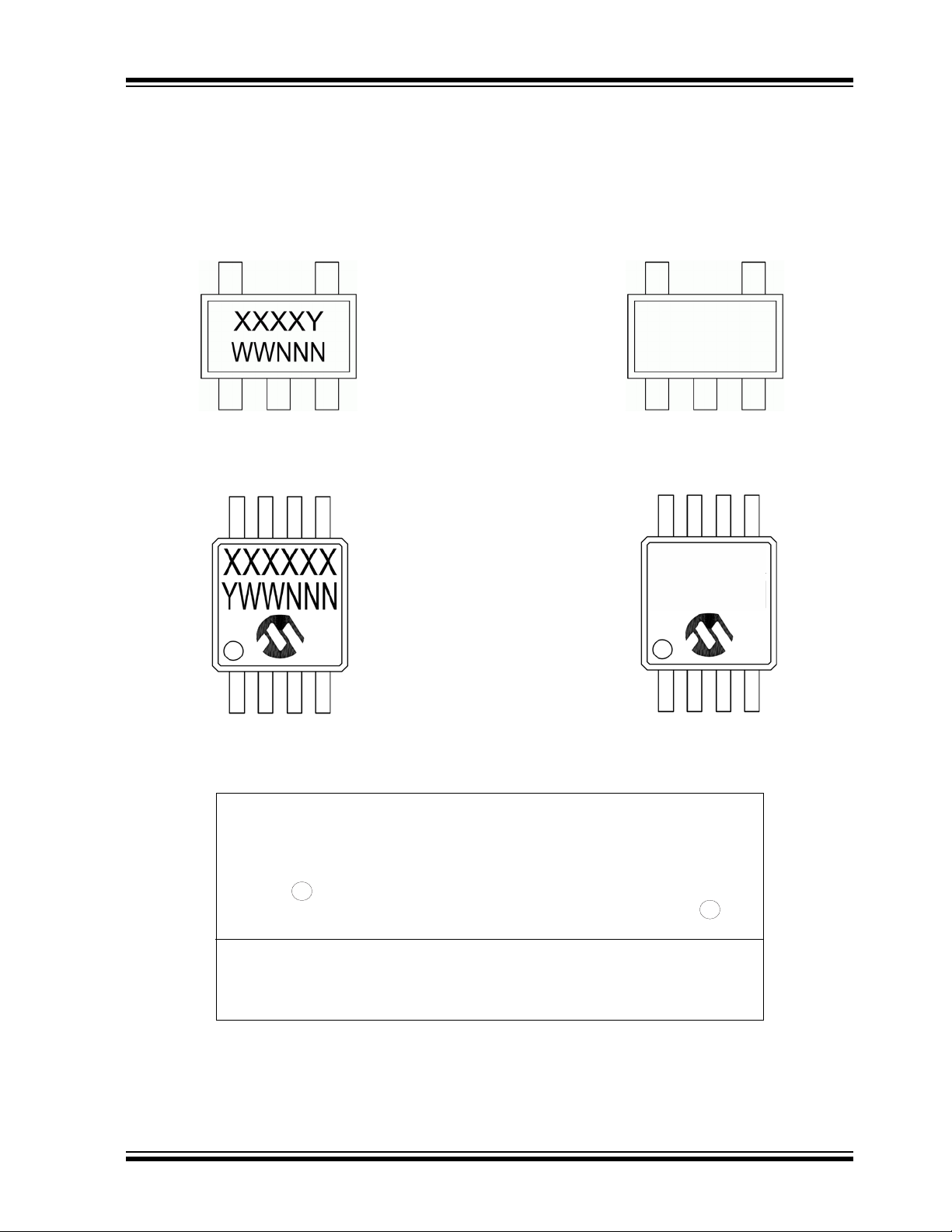
6.0 PACKAGING INFORMATION
Legend: XX...X Customer-specific information
Y Year code (last digit of calendar year)
YY Year code (last 2 digits of calendar year)
WW Week code (week of January 1 is week ‘01’)
NNN Alphanumeric traceability code
Pb-free JEDEC
®
designator for Matte Tin (Sn)
* This package is Pb-free. The Pb-free JEDEC designator ( )
can be found on the outer packaging for this package.
Note: In the event the full Microchip part number cannot be marked on one line, it will
be carried over to the next line, thus limiting the number of available
characters for customer-specific information.
3
e
5-Lead SOT-23 Example
AADQY
32256
6V51
832256
8-Lead MSOP
Example
6.1 Package Marking Information
MCP6V51
3
e
2018 Microchip Technology Inc. DS20006136A-page 31
Page 32

MCP6V51
0.15
C D
2X
NOTE 1
12
N
TOP VIEW
SIDE VIEW
Microchip Technology Drawing C04-091-OT Rev E Sheet 1 of 2
For the most current package drawings, please see the Microchip Packaging Specification located at
http://www.microchip.com/packaging
Note:
0.20
C
C
SEATING PLANE
A
A2
A1
e
NX bB
0.20 C A-B D
e1
D
E1
E1/2
E/2
E
D
A
0.20 C 2X
(DATUM D)
(DATUM A-B)
A
A
SEE SHEET 2
5-Lead Plastic Small Outline Transistor (OT) [SOT23]
DS20006136A-page 32 2018 Microchip Technology Inc.
Page 33

Microchip Technology Drawing C04-091-OT Rev E Sheet 2 of 2
For the most current package drawings, please see the Microchip Packaging Specification located at
http://www.microchip.com/packaging
Note:
c
L
L1
T
VIEW A-A
SHEET 1
5-Lead Plastic Small Outline Transistor (OT) [SOT23]
protrusions shall not exceed 0.25mm per side.
1.
BSC: Basic Dimension. Theoretically exact value shown without tolerances.
2.
Foot Angle
Number of Pins
Pitch
Outside lead pitch
Overall Height
Molded Package Thickness
Standoff
Overall Width
Molded Package Width
Overall Length
Foot Length
Footprint
Lead Thickness
Lead Width
Notes:
L1
I
b
c
Dimension Limits
E
E1
D
L
e1
A
A2
A1
Units
N
e
0°
0.08
0.20 -
-
-
10°
0.26
0.51
MILLIMETERS
0.95 BSC
1.90 BSC
0.30
0.90
0.89
-
0.60 REF
2.90 BSC
-
2.80 BSC
1.60 BSC
-
-
-
MIN
5
NOM
1.45
1.30
0.15
0.60
MAX
REF: Reference Dimension, usually without tolerance, for information purposes only.
Dimensions D and E1 do not include mold flash or protrusions. Mold flash or
Dimensioning and tolerancing per ASME Y14.5M
MCP6V51
2018 Microchip Technology Inc. DS20006136A-page 33
Page 34

MCP6V51
RECOMMENDED LAND PATTERN
5-Lead Plastic Small Outline Transistor (OT) [SOT23]
For the most current package drawings, please see the Microchip Packaging Specification located at
http://www.microchip.com/packaging
Note:
BSC: Basic Dimension. Theoretically exact value shown without tolerances.
Notes:
1. Dimensioning and tolerancing per ASME Y14.5M
Microchip Technology Drawing No. C04-2091B [OT]
Dimension Limits
Contact Pad Length (X5)
Overall Width
Distance Between Pads
Contact Pad Width (X5)
Contact Pitch
Contact Pad Spacing
3.90
1.10
G
Z
Y
1.70
0.60
MAXMIN
C
X
E
Units
NOM
0.95 BSC
2.80
MILLIMETERS
Distance Between Pads GX 0.35
1
5
X
Y
Z
C
E
GX
G
2
SILK SCREEN
DS20006136A-page 34 2018 Microchip Technology Inc.
Page 35

Note: For the most current package drawings, please see the Microchip Packaging Specification located at
http://www.microchip.com/packaging
MCP6V51
2018 Microchip Technology Inc. DS20006136A-page 35
Page 36

MCP6V51
Note: For the most current package drawings, please see the Microchip Packaging Specification located at
http://www.microchip.com/packaging
DS20006136A-page 36 2018 Microchip Technology Inc.
Page 37

Note: For the most current package drawings, please see the Microchip Packaging Specification located at
http://www.microchip.com/packaging
MCP6V51
2018 Microchip Technology Inc. DS20006136A-page 37
Page 38

MCP6V51
NOTES:
DS20006136A-page 38 2018 Microchip Technology Inc.
Page 39

APPENDIX A: REVISION HISTORY
Revision A (December 2018)
• Initial release of this document
MCP6V51
2018 Microchip Technology Inc. DS20006136A-page 39
Page 40

PRODUCT IDENTIFICATION SYSTEM
PAR T N O .
X
/XX
Package
Temperature
Range
Device
Device: MCP6V51: 45V, 2 MHz Zero-Drift Op Amp with EMI Filtering
Tape and Reel
Option:
Blank = Standard packaging (tube or tray)
T = Tape and Reel
(1)
Temperature
Range:
E= -40C to +125C (Extended)
Package: OT = 5-Lead Plastic Small Outline Transistor (SOT-23)
MS = 8-Lead Plastic Micro Small Outline Package
(MSOP)
Examples:
a) MCP6V51T-E/OT: 5-Lead SOT-23 package,
Tape and Reel
b) MCP6V51-E/MS: 8-Lead MSOP package
c) MCP6V51T-E/MS: 8-Lead MSOP package,
Tape and Reel
Note 1: Tape and Reel identifier only appears in the
catalog part number description. This
identifier is used for ordering purposes and is
not printed on the device package. Check
with your Microchip Sales Office for package
availability with the Tape and Reel option.
[X]
(1)
Tape and Reel
Option
To order or obtain information, e.g., on pricing or delivery, refer to the factory or the listed sales office.
MCP6V51
2018 Microchip Technology Inc. DS20006136A-page 40
Page 41

MCP6V51
NOTES:
DS20006136A-page 41 2018 Microchip Technology Inc.
Page 42

Note the following details of the code protection feature on Microchip devices:
YSTEM
CERTIFIED BY DNV
== ISO/TS 16949 ==
• Microchip products meet the specification contained in their particular Microchip Data Sheet.
• Microchip believes that its family of products is one of the most secure families of its kind on the market today, when used in the
intended manner and under normal conditions.
• There are dishonest and possibly illegal methods used to breach the code protection feature. All of these methods, to our
knowledge, require using the Microchip products in a manner outside the operating specifications contained in Microchip’s Data
Sheets. Most likely, the person doing so is engaged in theft of intellectual property.
• Microchip is willing to work with the customer who is concerned about the integrity of their code.
• Neither Microchip nor any other semiconductor manufacturer can guarantee the security of their code. Code protection does not
mean that we are guaranteeing the product as “unbreakable.”
Code protection is constantly evolving. We at Microchip are committed to continuously improving the code protection features of our
products. Attempts to break Microchip’s code protection feature may be a violation of the Digital Millennium Copyright Act. If such acts
allow unauthorized access to your software or other copyrighted work, you may have a right to sue for relief under that Act.
Information contained in this publication regarding device
applications and the like is provided only for your convenience
and may be superseded by updates. It is your responsibility to
ensure that your application meets with your specifications.
MICROCHIP MAKES NO REPRESENTATIONS OR
WARRANTIES OF ANY KIND WHETHER EXPRESS OR
IMPLIED, WRITTEN OR ORAL, STATUTORY OR
OTHERWISE, RELATED TO THE INFORMATION,
INCLUDING BUT NOT LIMITED TO ITS CONDITION,
QUALITY, PERFORMANCE, MERCHANTABILITY OR
FITNESS FOR PURPOSE. Microchip disclaims all liability
arising from this information and its use. Use of Microchip
devices in life support and/or safety applications is entirely at
the buyer’s risk, and the buyer agrees to defend, indemnify and
hold harmless Microchip from any and all damages, claims,
suits, or expenses resulting from such use. No licenses are
conveyed, implicitly or otherwise, under any Microchip
intellectual property rights unless otherwise stated.
Microchip received ISO/TS-16949:2009 certification for its worldwide
headquarters, design and wafer fabrication facilities in Chandler and
Tempe, Arizona; Gresham, Oregon and design centers in California
and India. The Company’s quality system processes and procedures
are for its PIC
devices, Serial EEPROMs, microperipherals, nonvolatile memory and
analog products. In addition, Microchip’s quality system for the design
and manufacture of development systems is ISO 9001:2000 certified.
®
MCUs and dsPIC® DSCs, KEELOQ
®
code hopping
QUALITY MANAGEMENT S
Trademarks
The Microchip name and logo, the Microchip logo, AnyRate, AVR,
AVR logo, AVR Freaks, BitCloud, chipKIT, chipKIT logo,
CryptoMemory, CryptoRF, dsPIC, FlashFlex, flexPWR, Heldo,
JukeBlox, KeeLoq, Kleer, LANCheck, LINK MD, maXStylus,
maXTouch, MediaLB, megaAVR, MOST, MOST logo, MPLAB,
OptoLyzer, PIC, picoPower, PICSTART, PIC32 logo, Prochip
Designer, QTouch, SAM-BA, SpyNIC, SST, SST Logo,
SuperFlash, tinyAVR, UNI/O, and XMEGA are registered
trademarks of Microchip Technology Incorporated in the U.S.A.
and other countries.
ClockWorks, The Embedded Control Solutions Company,
EtherSynch, Hyper Speed Control, HyperLight Load, IntelliMOS,
mTouch, Precision Edge, and Quiet-Wire are registered
trademarks of Microchip Technology Incorporated in the U.S.A.
Adjacent Key Suppression, AKS, Analog-for-the-Digital Age, Any
Capacitor, AnyIn, AnyOut, BodyCom, CodeGuard,
CryptoAuthentication, CryptoAutomotive, CryptoCompanion,
CryptoController, dsPICDEM, dsPICDEM.net, Dynamic Average
Matching, DAM, ECAN, EtherGREEN, In-Circuit Serial
Programming, ICSP, INICnet, Inter-Chip Connectivity,
JitterBlocker, KleerNet, KleerNet logo, memBrain, Mindi, MiWi,
motorBench, MPASM, MPF, MPLAB Certified logo, MPLIB,
MPLINK, MultiTRAK, NetDetach, Omniscient Code Generation,
PICDEM, PICDEM.net, PICkit, PICtail, PowerSmart, PureSilicon,
QMatrix, REAL ICE, Ripple Blocker, SAM-ICE, Serial Quad I/O,
SMART-I.S., SQI, SuperSwitcher, SuperSwitcher II, Total
Endurance, TSHARC, USBCheck, VariSense, ViewSpan,
WiperLock, Wireless DNA, and ZENA are trademarks of
Microchip Technology Incorporated in the U.S.A. and other
countries.
SQTP is a service mark of Microchip Technology Incorporated in
the U.S.A.
Silicon Storage Technology is a registered trademark of Microchip
Technology Inc. in other countries.
GestIC is a registered trademark of Microchip Technology
Germany II GmbH & Co. KG, a subsidiary of Microchip
Technology Inc., in other countries.
All other trademarks mentioned herein are property of their
respective companies.
© 2018, Microchip Technology Incorporated, All Rights Reserved.
ISBN: 978-1-5224-3968-4
2018 Microchip Technology Inc. DS20006136A-page 42
Page 43

Worldwide Sales and Service
AMERICAS
Corporate Office
2355 West Chandler Blvd.
Chandler, AZ 85224-6199
Tel: 480-792-7200
Fax: 480-792-7277
Technical Support:
http://www.microchip.com/
support
Web Address:
www.microchip.com
Atlanta
Duluth, GA
Tel: 678-957-9614
Fax: 678-957-1455
Austin, TX
Tel: 512-257-3370
Boston
Westborough, MA
Tel: 774-760-0087
Fax: 774-760-0088
Chicago
Itasca, IL
Tel: 630-285-0071
Fax: 630-285-0075
Dallas
Addison, TX
Tel: 972-818-7423
Fax: 972-818-2924
Detroit
Novi, MI
Tel: 248-848-4000
Houston, TX
Tel: 281-894-5983
Indianapolis
Noblesville, IN
Tel: 317-773-8323
Fax: 317-773-5453
Tel: 317-536-2380
Los Angeles
Mission Viejo, CA
Tel: 949-462-9523
Fax: 949-462-9608
Tel: 951-273-7800
Raleigh, NC
Tel: 919-844-7510
New York, NY
Tel: 631-435-6000
San Jose, CA
Tel: 408-735-9110
Tel: 408-436-4270
Canada - Toronto
Tel: 905-695-1980
Fax: 905-695-2078
ASIA/PACIFIC
Australia - Sydney
Tel: 61-2-9868-6733
China - Beijing
Tel: 86-10-8569-7000
China - Chengdu
Tel: 86-28-8665-5511
China - Chongqing
Tel: 86-23-8980-9588
China - Dongguan
Tel: 86-769-8702-9880
China - Guangzhou
Tel: 86-20-8755-8029
China - Hangzhou
Tel: 86-571-8792-8115
China - Hong Kong SAR
Tel: 852-2943-5100
China - Nanjing
Tel: 86-25-8473-2460
China - Qingdao
Tel: 86-532-8502-7355
China - Shanghai
Tel: 86-21-3326-8000
China - Shenyang
Tel: 86-24-2334-2829
China - Shenzhen
Tel: 86-755-8864-2200
China - Suzhou
Tel: 86-186-6233-1526
China - Wuhan
Tel: 86-27-5980-5300
China - Xian
Tel: 86-29-8833-7252
China - Xiamen
Tel: 86-592-2388138
China - Zhuhai
Tel: 86-756-3210040
ASIA/PACIFIC
India - Bangalore
Tel: 91-80-3090-4444
India - New Delhi
Tel: 91-11-4160-8631
India - Pune
Tel: 91-20-4121-0141
Japan - Osaka
Tel: 81-6-6152-7160
Japan - Tokyo
Tel: 81-3-6880- 3770
Korea - Daegu
Tel: 82-53-744-4301
Korea - Seoul
Tel: 82-2-554-7200
Malaysia - Kuala Lumpur
Tel: 60-3-7651-7906
Malaysia - Penang
Tel: 60-4-227-8870
Philippines - Manila
Tel: 63-2-634-9065
Singapore
Tel: 65-6334-8870
Taiwan - Hsin Chu
Tel: 886-3-577-8366
Taiwan - Kaohsiung
Tel: 886-7-213-7830
Taiwan - Taipei
Tel: 886-2-2508-8600
Thailand - Bangkok
Tel: 66-2-694-1351
Vietnam - Ho Chi Minh
Tel: 84-28-5448-2100
EUROPE
Austria - Wels
Tel: 43-7242-2244-39
Fax: 43-7242-2244-393
Denmark - Copenhagen
Tel: 45-4450-2828
Fax: 45-4485-2829
Finland - Espoo
Tel: 358-9-4520-820
France - Paris
Tel: 33-1-69-53-63-20
Fax: 33-1-69-30-90-79
Germany - Garching
Tel: 49-8931-9700
Germany - Haan
Tel: 49-2129-3766400
Germany - Heilbronn
Tel: 49-7131-67-3636
Germany - Karlsruhe
Tel: 49-721-625370
Germany - Munich
Tel: 49-89-627-144-0
Fax: 49-89-627-144-44
Germany - Rosenheim
Tel: 49-8031-354-560
Israel - Ra’anana
Tel: 972-9-744-7705
Italy - Milan
Tel: 39-0331-742611
Fax: 39-0331-466781
Italy - Padova
Tel: 39-049-7625286
Netherlands - Drunen
Tel: 31-416-690399
Fax: 31-416-690340
Norway - Trondheim
Tel: 47-7288-4388
Poland - Warsaw
Tel: 48-22-3325737
Romania - Bucharest
Tel: 40-21-407-87-50
Spain - Madrid
Tel: 34-91-708-08-90
Fax: 34-91-708-08-91
Sweden - Gothenberg
Tel: 46-31-704-60-40
Sweden - Stockholm
Tel: 46-8-5090-4654
UK - Wokingham
Tel: 44-118-921-5800
Fax: 44-118-921-5820
DS20006136A-page 43 2018 Microchip Technology Inc.
08/15/18
 Loading...